1. Introduction
Boron-based coatings are promising protective surface coatings [
1]. They are used to harden the surface of parts and structural materials in the field of mechanical engineering [
2]. They are characterized by high hardness, resistance to wear [
3], corrosion [
4], and high thermal stability [
5]. For example, wurtzite boron nitride has comparable hardness to natural diamond [
6]. Pure boron thin films are used as materials in electronic [
7] and optical devices [
8] as well as in protective layers of thermonuclear installations [
9]. Moreover, boron coatings of monoisotopic compositions find applications in the nuclear industry; for example,
10B-based coatings are promising as burnable neutron absorbers in nuclear reactors [
10] and as absorber coatings of neutron detectors [
11]; they are also used for the delivery of
10B atoms deposited on the surface of nanosized particles to the malignant neoplasm during boron neutron capture therapy [
12], while
11B-based coatings are used for the
11B aneutronic fusion of protons and
11B atomic nuclei, which may be an alternative to deuterium and tritium fusion [
13]. Hence, developing techniques to deposit boron coatings, investigating the properties of boron coatings, and revealing the interrelationship between these properties and conditions that brought about their formation are crucial.
Boriding is an industrial technique that has been used widely for decades to develop boron-containing layers on metal and alloy surfaces. In this process, boride atoms are diffused into the surface of a metal component, resulting in the formation of metal borides in the surface layer, thereby increasing the surface hardness and wear resistance. Conventional boriding can be achieved in a solid, liquid, or gaseous [
14,
15] medium [
16,
17]. However, there are disadvantages to using it, including the high energy consumption required for heating parts and electrolysis of boron-containing media, the long duration of surface diffusive saturation with boron, the use of hazardous and toxic substances, and environmental pollution.
Vacuum-plasma methods, such as magnetron sputtering [
18,
19] or cathodic arc deposition [
20,
21,
22], can be used as alternatives for creating boron surface layers owing to their eco-friendliness because the equipment of this type generates a boron flux from a consumable boron-containing solid cathode during an electric discharge in a vacuum chamber. Moreover, there is no heating requirement for the surface because the main process involves the deposition of boron atoms or ions onto the surface. Another advantage of these methods over conventional boriding is the short process duration, which is determined by the flux intensity. The maximum flux intensity is limited by thermal stability in the discharge of the consumed boron-containing cathode. At maximum discharge parameters, the deposition rate of boron-containing coatings at a characteristic distance of 10 cm from the cathode can reach approximately 20–30 nm/min [
19] for magnetron sputtering and approximately 100 nm/min for arc deposition [
22].
A method for depositing boron coating has been proposed based on the electron beam evaporation of a boron solid target using an electron beam at a fore-vacuum pressure [
23]. Briefly, a boron or boron-containing ceramic target is heated locally by an electron beam to the melting temperature and the melted surface area undergoes an intense evaporation. The flux of boron vapor, partially ionized by the beam, deposits onto the substrate surface forming a boron-containing coating [
24]. The maximum temperature of the boron-containing target is limited in this case not by its thermal resistance, as in magnetron or vacuum arc deposition of boron coatings [
18,
19,
20,
21,
22] but by the temperature of intense boiling of boron, at which an unwanted flux of droplets occurs because of the splashing of the molten target material. Thus, the boron coating deposition rate under this method is much higher than that under magnetron sputtering or arc deposition and can reach up to 1 µm/min [
24], which provides a higher coating production performance. This work aims to further develop this method using an additional action of a wide-aperture electron beam in the fore-vacuum on the deposited boron coating. The characteristics and properties of boron coatings are studied by surface analysis, which includes structural phase analysis with synchrotron radiation generated by the VEEP-2 electron storage ring based in the Siberian Center for Synchrotron and Terahertz Radiation at G. I. Budker Institute of Nuclear Physics, SB of RAS [
25].
2. Experimental Setup and Diagnostics
Figure 1 illustrates the setup for depositing boron coatings by electron-beam heating and evaporation of a crystal boron target. The target was evaporated using a fore-vacuum plasma electron source operating in continuous mode [
26]. In such a source, electrons are extracted from a hollow cathode glow discharge plasma. The discharge current varies from 100 to 500 mA, while the discharge burning voltage, depending on the discharge current and gas pressure, varies from 200 to 500 V. At the maximum discharge current, the source is capable of generating electron beams with a current of up to 200 mA and energy of up to 20 keV, while the beam can be focused on the target surface by the magnetic field of the focusing system to a diameter of 3 mm. The electron beam current is controlled by the discharge current. The average power density in the electron beam focal spot on the target surface is 500 W/mm
2, which is several times greater than the radiation power density on the sun’s surface (approximately 60 W/mm
2). Hence, the source is capable of melting and evaporating the surface of a target composed of any refractory material.
A 4-mm-thick, 1 × 1 cm2 boron plate target fabricated using the hot pressing of 99.6% pure boron crystals 1–10 µm in size was placed at the bottom of the vacuum chamber on a carbon crucible. The average density of the target due to the pores between crystals was 1.2 g/cm3, which is two times less than the density of amorphous boron. Because the pores occupied 50% of the target volume, the effective surface-to-volume ratio for the target material was about 3 × 103 cm−1 and the total effective surface area of the target was about 0.1 m2. The electron beam toward the boron target was transported through the vacuum chamber filled with 99.9% pure nitrogen at a pressure of 10 Pa. An ISP-500C helical mechanical oil-free fore-vacuum pump with a pumping rate of 500 l/min was used to maintain the vacuum in the chamber. Prior to the experiment, the vacuum chamber was evacuated to a residual pressure of 1 Pa.
Because boron is a wide-gap semiconductor, its specific resistivity is as high as 1 MOhm × cm at a normal temperature of 20 °C; [
27], which is insufficient for the complete drain of the electron beam charge. Therefore, at the initial heating of the boron target, its negative surface charge introduced by the electron beam was neutralized by a flux of positive ions from the beam plasma [
28]. As the beam heated up the boron target, its specific resistivity decreased to 0.1 Ohm × cm at a temperature of about 750 °C. At this resistivity, the effect of the target surface charging by the beam becomes immaterial because of the electron beam current running through the boron target volume.
To prevent the boron target from thermal shock destruction, the target was heated in two stages, the parameters of which were determined experimentally [
24]. Initially, the electron beam with a current of 80 mA at an accelerating voltage of up to 5 kV heated up the target to a temperature of approximately 900 °C for 70 s. Subsequently, the accelerating voltage was increased slowly up to 9 kV for 1 min; in this case, there was an observed local melting of the target surface at the focal spot of the beam. Target evaporation occurred and the boron coating was deposited on the sample surface at a temperature of the melting pool of approximately 2400 °C, and after increasing the accelerating voltage to 10 kV and the beam current to 100 mA.
The samples with polished surfaces on which boron coatings were applied were disks of A284 steel and a special reactor alloy ZrNb1 with a hexagonal crystal lattice; they had a 2 cm diameter and 0.5 cm thickness. The samples were placed at an angle of 30° relative to the electron beam propagation axis. The sample surfaces were normally oriented to the center of the evaporated target. A high-performance Raytek-MM1MH optical pyrometer was used to monitor the temperature of the sample surface during the deposition process; the temperature did not exceed 500 °C. Plasma composition during the coating was controlled with a quadrupole mass analyzer based on an RGA-300 residual gas analyzer. We have produced several dozen samples with boron coating thicknesses of 1–7 µm throughout the course of our research. Herein, for comparison, we analyze coatings fabricated under the same conditions, such as a distance of 10 cm from the beam-heated boron target to the sample surface and an overall coating deposition time of 6 min and 10 s. Considering that the first two heating stages under which the deposition did not occur took 1 min and 10 s, the direct deposition time was 5 min.
The deposition rate of boron coatings by a 1 kW electron beam was measured with an MII-4 interferometer and an MNL-1 interference microscope-profilometer. The thickness of the deposited boron coatings was about 2.1 µm. Thus, under the experimental conditions, the coating growth rate was about 0.5 µm/min. The weight gain because of boron coating deposition, measured with a VL-220M analytical balance with a precision of ±10 µg, was 1.45 mg. Considering a sample surface area of 3.13 cm2, the density of boron coatings was estimated to be ρ ≈ 2.2 g/cm3, which is close to the density of crystalline boron of 2.34 g/cm3.
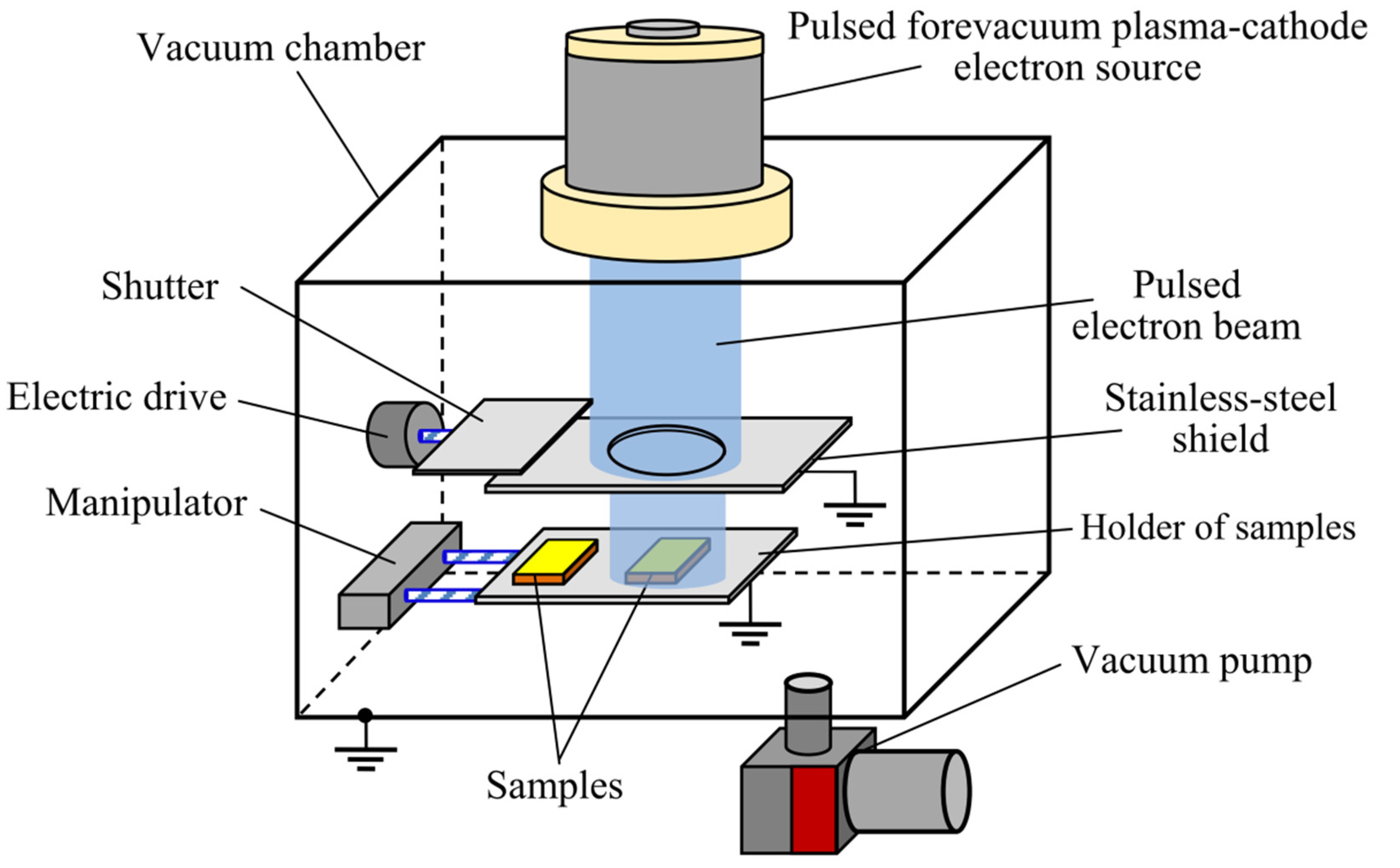
Figure 2 shows a setup for the modification of boron coatings obtained with a pulsed electron beam. The pulsed electron beam was generated by a fore-vacuum plasma-cathode electron source based on an arc discharge [
29]. The electron source was mounted on the vacuum chamber, which was evacuated with an ISP-500C pump. The working gas was helium at a pressure of 10 Pa. The samples were placed on a movable grounded holder, which allowed several samples to be sequentially irradiated after the chamber evacuation. To prevent the sample surface from beam exposure, a protective stainless-steel screen was applied on top of one of the samples. The treatment of boron-coated samples was performed in two regimes through a series of 300 pulses with a repetition rate of 2 pulses per second (p.p.s.). The length of each pulse was
= 500 µs. The beam diameter was 7 cm. In regime 1, the treatment was performed at a beam current amplitude of 20 A and an electron energy of 8 keV; in regime 2, it was performed at a beam current amplitude of 30 A and an electron energy of 6 keV. The electron current density
on the boron coating surface and the energy per pulse
were 0.5 A/cm
2 and 2 J/cm
2 for regime 1, and 0.75 A/cm
2 and 2.25 J/cm
2 for regime 2, respectively. The pulsed beam parameters for modifying the boron coatings were selected empirically: on the one hand, they should lead to a noticeable change in the surface morphology; on the other hand, they should be soft enough to prevent the coating from cracking, or its evaporation.
The morphology of the final coatings was studied using a Hitachi S3400N scanning electron microscope and a Solver P47 atomic force microscope. Elemental composition was analyzed with a Bruker X’Flash 5010 energy dispersive spectrometer. The surface hardness of coatings was determined using the micro-Vickers technique. A square-section diamond indenter with a dihedral angle of 136° acted on the sample surface at various points with a constant load of 100 g while the penetration depth and indentation area were recorded. The phase composition of coatings was measured at the Synchrotron Radiation Station for High-Precision X-ray Diffraction Studies of Materials (also called the “Anomalous Scattering” station) on beamline No. 2 of the VEPP-3M electron storage ring at the Siberian Synchrotron Radiation Center (Budker Institute of Nuclear Physics, SB of RAS).
For the evaluation of the adhesive properties of the coatings, the scratch method was used. The method consisted of applying a force F (linearly growing with time) to the diamond indenter with its simultaneous uniform displacement along the coating surface. At the critical load Fc, the coating begins to break down. The critical load Fc is determined using the sensors of acoustic emission and friction force, indenter immersion depth, indenter loading force, and optical microscopy.
Adhesion can be characterized by a parameter
G (specific peel work). The calculation formula connecting the parameter
G with the critical lateral load
Fc at the beginning of the film detachment from the substrate is as follows:
where
d is the film thickness;
rc is the radius of the contact spot at the moment of peeling;
EIT is the Young’s modulus of the substrate material. The determination of adhesion was carried out using a Micro-Scratch Tester MST-S-AX-0000 device.
The wear resistance of the obtained coatings was measured using a Pinon Disc and Oscillating TRIBO tester (France) using the “ball on disk” method. The sample surface was pressed by a tungsten carbide spherical tip with a load of 2 N. The coefficient of friction was determined by measuring the deflection of the lever. The wear rate was calculated by the formula:
where
R is the track radius, µm;
A is the cross-sectional area of the wear groove, µm
2;
F is the value of the applied load, N;
L is the distance traveled by the ball, m.
3. Results and Discussion
During the target heating and coating deposition, the ion composition of the plasma was measured with a quadrupole mass spectrometer based on an RGA-300 residual gas analyzer [
30]. In our previous work [
31], at an electric beam power of 0.4 kW, which corresponds to the preheating of the target at a beam current of 80 mA and an electron energy of 5 keV, the density of such a plasma is about 3 × 10
10 cm
−3. Initially, at the target heating, in addition to nitrogen ions, a significant number of ions, up to 50% of the total ions, were produced through water vapor ionization processes: HO
+, H
2O
+, and water dissociation products O
+, H
3+, H
2+, and H
+. The sources of water molecules were the walls of the vacuum chamber with a surface area of approximately 1 m
2, the overall effective surface of the boron crystalline target with dimensions 1 × 1 × 0.4 cm, and the total area of about 0.1 m
2. The appearance of water molecules on the walls and in the target was due to their exposure to the atmosphere prior to the experiments. With the electron beam power increasing to 0.7 kW, the surface temperature of the boron target at the beam focal spot reached 2100 °C; this started the melting process, and the plasma spectrum recorded traces of
10B
+ and
11B
+ ions. At this temperature, water molecules apparently evaporated from the target and the heated walls, resulting in the appearance of peaks of water vapor ions and their derivatives.
A further increase in the electron beam power of up to 1 kW led to an increase in the target temperature at the focal spot to 2400 °C. Consequently, a brightly glowing melt area about 4 mm in diameter formed on the target surface, from which an intense evaporation of boron occurred. In this case, the plasma density increased to approximately 1.6 × 1011 cm−3. The fraction of boron ions in this plasma, evaluated by the height of its ion peaks in the spectrometer signals, was approximately 75%, and their total density in the plasma was about 1.2 × 1011 cm−3. The ratio of 10B+ to 11B+ isotopes in the plasma at a beam power of 1 kW was 1:4, which is close to their natural ratio. Thus, the concentrations of 10B+ and 11B+ in the beam plasma were 2.4 × 10¹⁰ and 9.6 × 1010 cm−3, respectively.
Because boron coatings are formed from two-phase states, namely, plasma and boron vapor, it is important to know the contribution of each phase in coating formation. Because the thickness, elemental composition, and specific density of coatings were determined using independent methods, one can demonstrate that to form such boron coatings, the flux density of atomic and ion boron onto the sample surface must be approximately 9.6 × 1016 cm−2 s−1. The speed of boron isotope ions of mass Mi that leave the beam plasma with plasma electron temperature Te, in eV units, is determined by the ambipolar speed of sound . At Te ≈ 3 eV, this speed is 5.4 × 105 cm/s for 10B+ ions and 5.2 × 105 cm/s for 11B+ ions. Because only singly charged ions were registered in the beam plasma, the flux density of 10B+ ions on the sample surface equaled the product of their density in the plasma and their speed from plasma, which is 1.3 × 1016 cm−2 s−1. This value was 5.0 × 1016 cm−2 s−1 for the 11B+ isotope. Thus, the flux density of all boron ions on the sample surface was around 6.3 × 1016 cm−2 s−1. Comparing this value with the above estimate of the total boron particle flux both in ionized and neutral states, it was concluded that the contribution of the plasma phase to the formation of boron coatings is about 65 at.%, which exceeds the 35 at.% contribution of boron vapor.
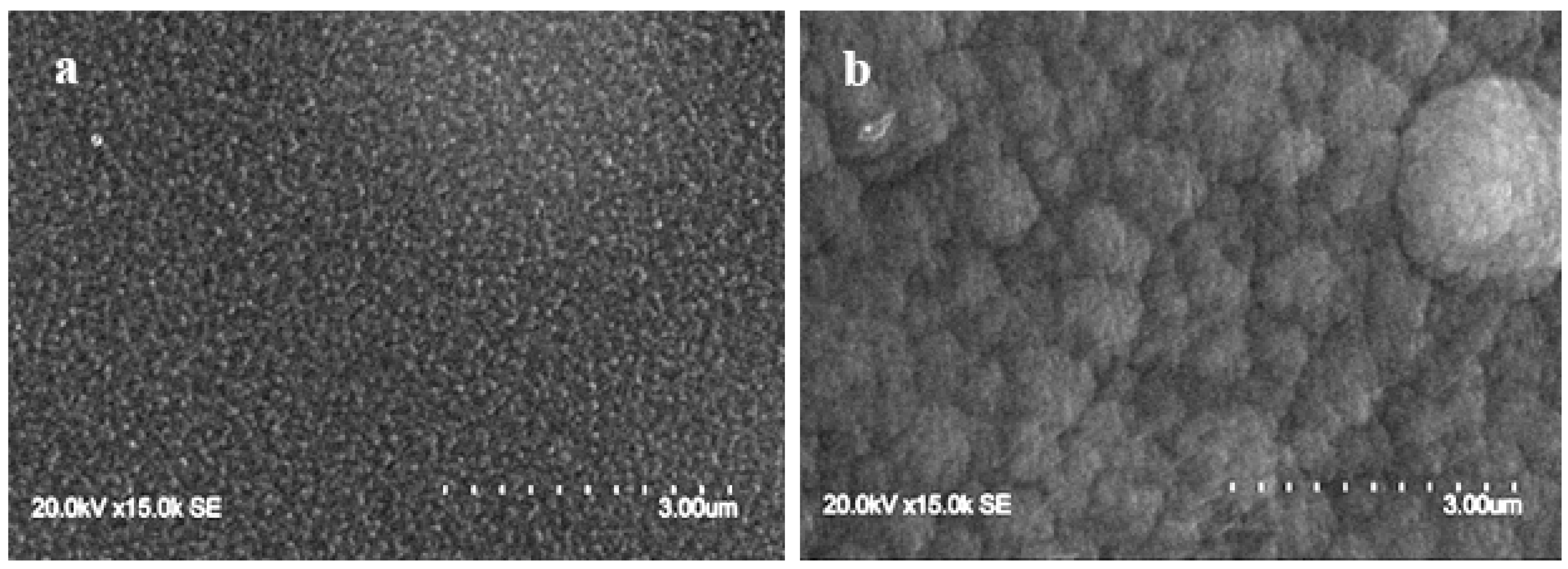
Figure 3 shows the scanning electron microscopy (SEM) images of the surfaces of the obtained boron coatings. The coatings do not contain any defects, pores, or cracks, indicative of coating uniformity and smoothness. The boron coating deposited without the electron beam comprises small tightly packed segments 30–150 nm in size, while that deposited with a pulsed electron beam (regime 1) has a structure with discernible round hills on the surface. The characteristic side of the hill base in the image field is approximately 1–3 µm.
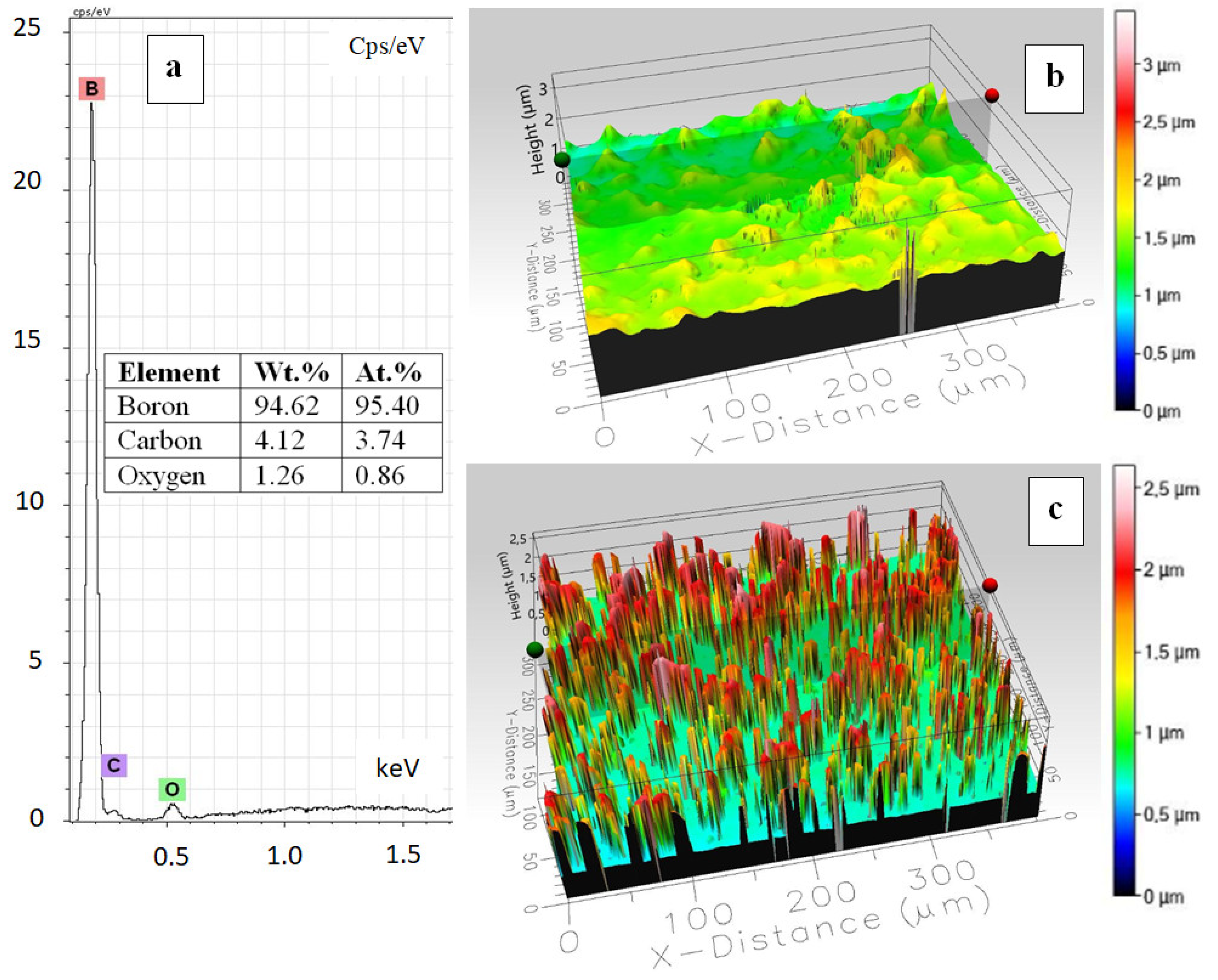
Figure 4a shows the elemental composition of the coating, comprising 95.5 at.% boron with small admixtures of carbon (3.7 at.%) and oxygen (0.9 at.%). Analysis of the elemental composition of coatings modified and unmodified by the electron beam showed that beam treatment did not practically change the coating composition. The carbon content in the coating is caused by the presence of this element in the substrate material (steel A284).
Figure 4b,c shows the coating profiles measured using a Solver P47 SEM before and after treatment with a pulsed electron beam in regime 2. For a better visual perception of the beam effect, the scale of the height axes in
Figure 4b,c is two orders of magnitude smaller than the scales of width and length, and the columnar structure of the surface in
Figure 4c is actually a landscape of gently sloping hills. Hence, the deposition of coating forms a relatively smooth surface with nonuniformities a few fractions of a micrometer in size, while subsequent treatment by a pulsed electron beam leads to the formation of gentle hills with a height of up to 1.5 µm. In contrast to SEM, the use of atomic force microscopy (AFM) to determine the surface relief may screen small nonuniformities adjacent to the larger ones with a larger height. Thus,
Figure 4b shows mostly hills with a base diameter of 1–10 µm although their structure qualitatively matches the surface structure in
Figure 3b with discernible smaller hills. The change in energy during the pulse action on the coating does not significantly affect the picture of the surface; however, the size and height of the hills in regime 1 are approximately 20% greater than those in regime 2.
Accelerated electrons in a solid are decelerated in the layer of their maximal range of penetration. Based on previous works [
32], this range
Re in micron units at an electron beam energy
Ee = 0.5–10 keV in a solid with density ρ (in g/cm
3) with an accuracy of better than 15% can be estimated by
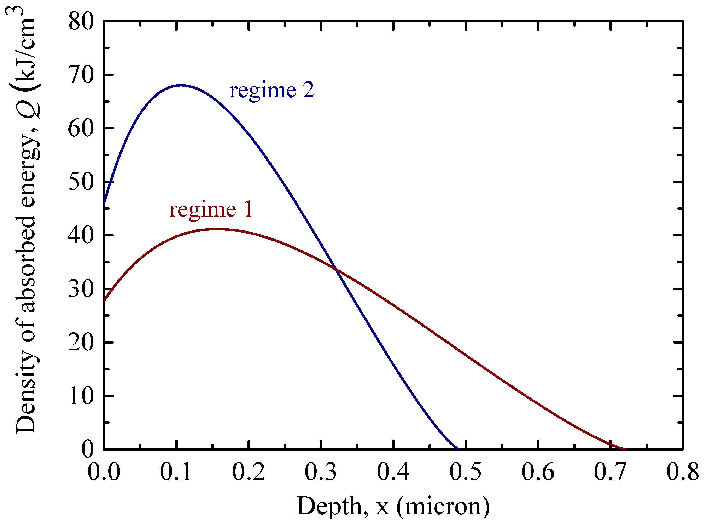
For boron coating ρ ≈ 2.2 g/cm3 and electron beam energy Ee = 8 keV, the value of Re is 0.72 µm for regime 1, while for Ee = 6 keV, the Re value is 0.49 µm for regime 2. Thus, for both regimes, the electron energy is released in the layer whose thickness is less than that of the boron coating.
The dependence of energy density distribution
Q absorbed from the beam of accelerated electrons by the boron coating at depth
x can be determined by [
33]
where
and
are the densities of the electron beam current on the sample surface and the pulse duration, respectively, and Z = 5 is the number of electrons in a boron atom. When evaluating
, it is convenient to substitute in the first factor in Expression (2), the electron energy
in eV and
in cm, and the remaining factors should use
in µm. In this case, the
Q value is expressed in J/cm
3 and the depth
x is expressed in µm. The dependences of the energy density distribution for the electron beam in both regime 1 and regime 2 are shown in
Figure 5.
The boron temperature profile with depth
x will approximately match the profile of
, provided that the condition
holds true, where
0.1 cm
2/s is the thermal diffusivity of the boron coating. At experimental electron energies, this condition is strictly satisfied for submicrosecond electron beam pulses, when the heat due to the energy imparted from the beam at a depth
Re does not have time to propagate deep into the surface of the solid. However, even though this condition is not satisfied in our experimental conditions due to much longer pulse width (hundreds of microseconds), anyway, as follows from the dependences in
Figure 5, about 70% of the released energy of accelerated electrons and, therefore, the most intense heating of the coating material occurs at a depth of 0.5
Re, which corresponds to 17% of the overall coating thickness at
Ee = 8 keV and about 12% at
Ee = 6 keV. That means that a significant part of electron beam energy can be deposited even at much longer pulses. Moreover, because the experimental processing of coatings was performed using a series of 300 pulses for 150 s, it is possible that the gradual heating of the coating surface during this period of time took place.
The surface hilly structure appeared due to the beam action, which is apparently related to cyclic temperature effects. The energy density of the pulsed electron beam on the coating surface is about 2 J/cm
2 per pulse, while the thermal conductivity coefficient of boron is an order of magnitude less than those of the majority of metals. Thus, the surface of the boron coating at the depth with the maximum release of the beam energy can heat up to a temperature at which the thin surface layer of the coating begins to melt. A similar relief of the surface of TiNi alloy was observed during repeated treatment by an electron beam with an electron energy of 20 keV and a beam power per pulse of 4 J/cm
2 [
34]. Under the beam action, a hilly structure was formed; the number of pulses (128) in this case was comparable to that in our experiments (300 pulses). From a prior study [
32], such surface relief may be associated with the development of instabilities on the melt/vapor phase interface under repeated action of the electron beam and cyclic melting and cooling of a thin surface layer. Similar effects seem to take place in our case too. Another thing that can be noted is that the pulsed electron beam treatment may have an effect on the structure of the deposited coating at different depths. Although the study of such effects is an interesting task, it was outside of the scope of the current research focused on the study of the surface properties of the coating.
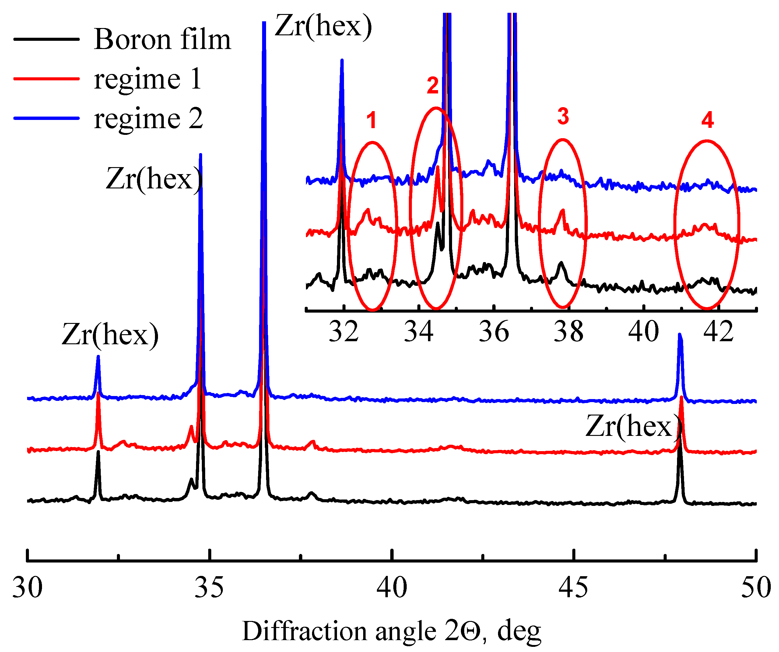
The structural phase properties of boron coatings were studied using synchrotron radiation on beamline 2 of the VEPP-3 electron storage ring at the Anomalous Scattering station. In the X-ray diffraction patterns of boron coatings treated and untreated with the electron beam, reflections of low intensity and considerable width are observed. Among them, there are two remarkable reflections that correspond to interplanar distances of 0.27 and 0.24 nm (areas 1, 2, 3, and 4 in the inset of
Figure 6). These reflections are associated with ultrafine crystals of nonstoichiometric boron nitride. Notably, these reflections decrease for regime 2, which may be indicative of the partial destruction of crystals by the beam with a high power density. However, the X-ray patterns do not show any reflections that can be associated with the crystal structure of boron, as is the case for the hexagonal crystal structure of the zirconium alloy. Thus, the hilly surface of the boron coating after the beam treatment does not exhibit a pronounced inner crystalline structure, and the hills themselves are not specific crystalline formations. This fact again verifies the nature of their formation as a result of repeated melting and cooling of the coating surface at the depth of the maximum beam energy release during the cyclic beam action.
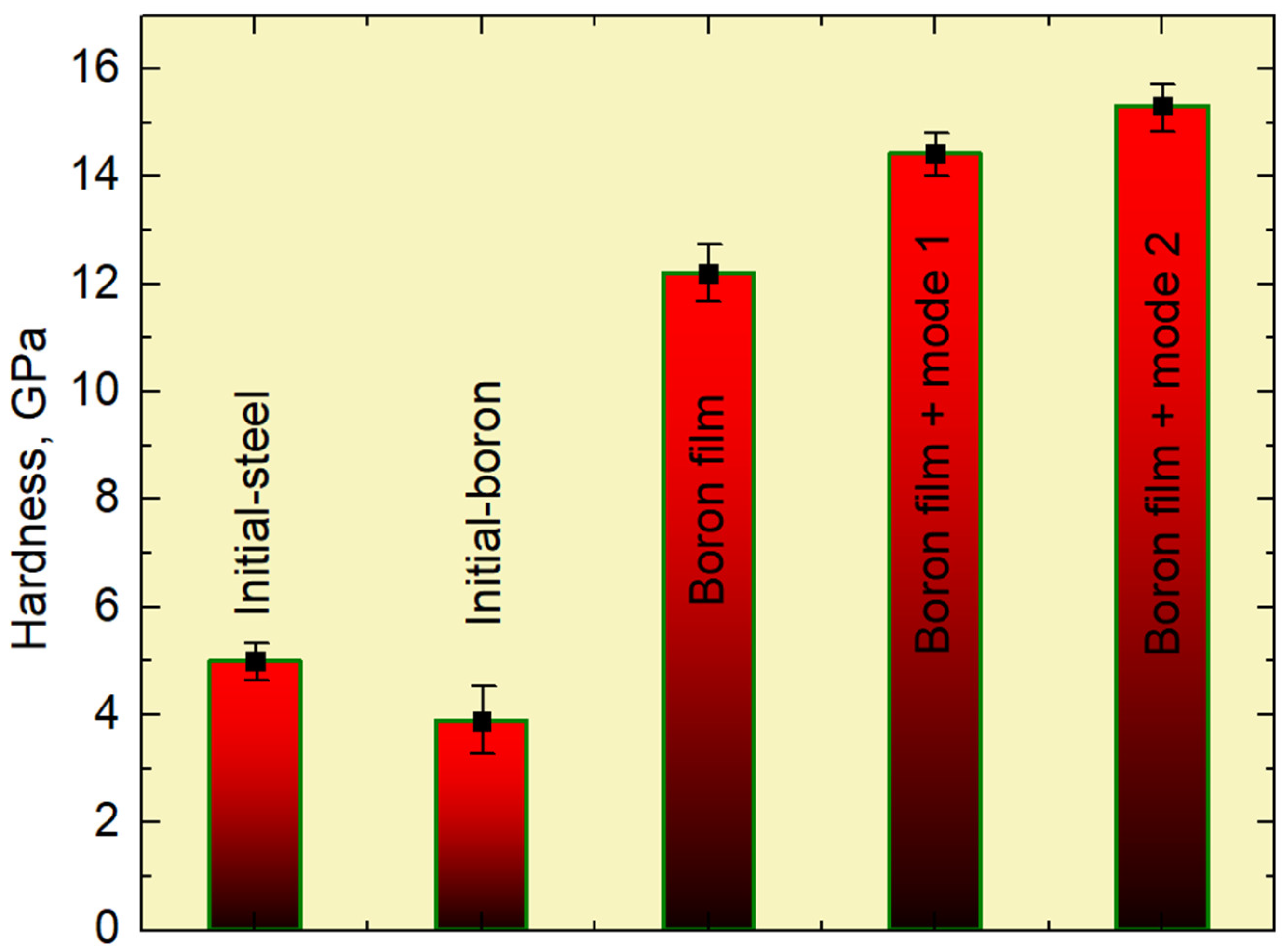
Figure 7 shows the microhardness results of a steel substrate, a crystalline boron target, boron coatings, and boron coatings treated with a pulsed electron beam (regime 1, regime 2). The microhardness of the crystalline boron target is approximately three times less than that of the boron coating. This is apparently due to the density of the target (1.2 g/cm
3) being lower than the measured density of the coating (2.2 g/cm
3). The microhardness of the boron coating is 12 ± 0.35 GPa, while additional surface modification with a pulsed beam further increases the microhardness, up to 15.5 ± 0.45 GPa.
The adhesion measurements of the samples with boron-based coatings showed that the pulsed beam treatment of coatings did not affect the adhesion value between the boron coating and the sample surface. This is because the beam mainly affected the surface layers of the coating as adhesion is the interface property of the coating–substrate boundary on which the effect of beam treatment was weak.
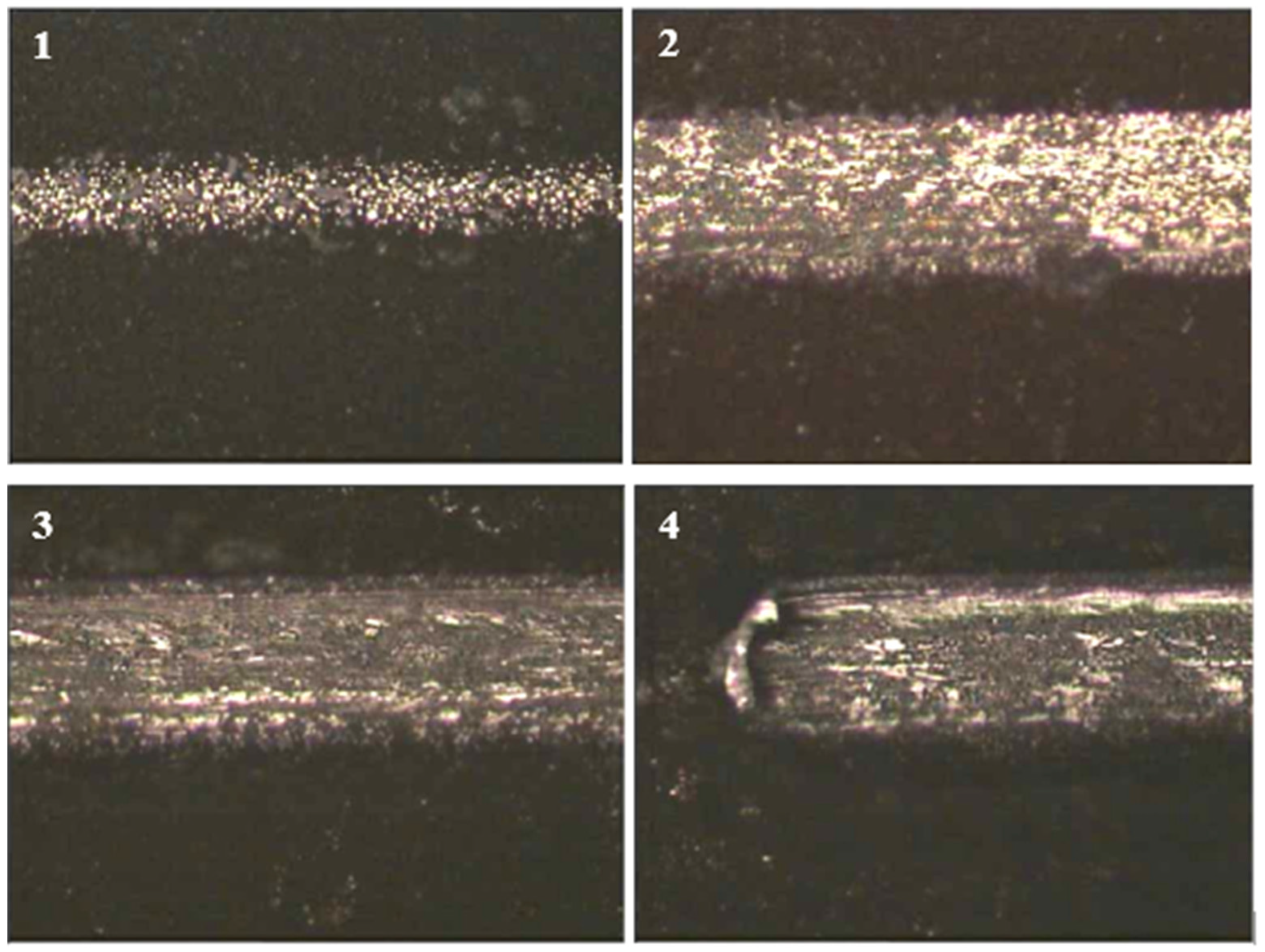
Figure 8 shows the typical micrographs of the surface under different loads
F exerted on a diamond indenter with a radius of 100 µm. As the pressure on the indenter increases, it begins to submerge into the coating. This is accompanied by an increase in the coefficient of friction, indicating the growing resistance of the sample to the indenter movement. At a load of 6 N exerted on the coating, the coefficient of friction begins to fluctuate, which is indicative of the destruction of the surface structure. In the micrograph of the 6 N load, the start of the local film peeling can be seen. A further increase in the load on the indenter leads to increased fluctuations in the coefficient of friction and in the submergence depth, which is indicative of the film peeling off the substrate. The maximum load on the indenter was 30 N; nevertheless, it sufficed to completely peel off the coating. Traces of the coating remained on the substrate surface. Thus, it can be estimated that the specific peel work of the coating was about 100 J/m
2.
The wear resistance of the A284 steel samples with deposited boron coatings and the samples with the same coatings modified by a pulsed electron beam was also measured. The wear rate of the original sample was 6 × 10⁻⁴ mm3/N·m, while that of the boron-based coating sample was significantly lower and equal to 0.8 × 10⁻⁴ mm3/N·m. The wear rate of the coating modified by the pulsed electron beam was 1.3 × 10⁻⁴ mm3/N·m, lower than that for the uncoated samples but higher than that for the boron coating without beam treatment. Thus, the boron-based coating increases the surface wear resistance by a factor of 7.5, but the coating modification by a pulsed electron beam rolls it back by about 60%. Meanwhile, even a surface with boron coating modified by the beam has a wear resistance 4.5 times higher than that without coating. In our opinion, the reduced wear resistance of the boron coating after modification is associated with an increase in the coefficient of friction due to the formation of the surface hilly structure.
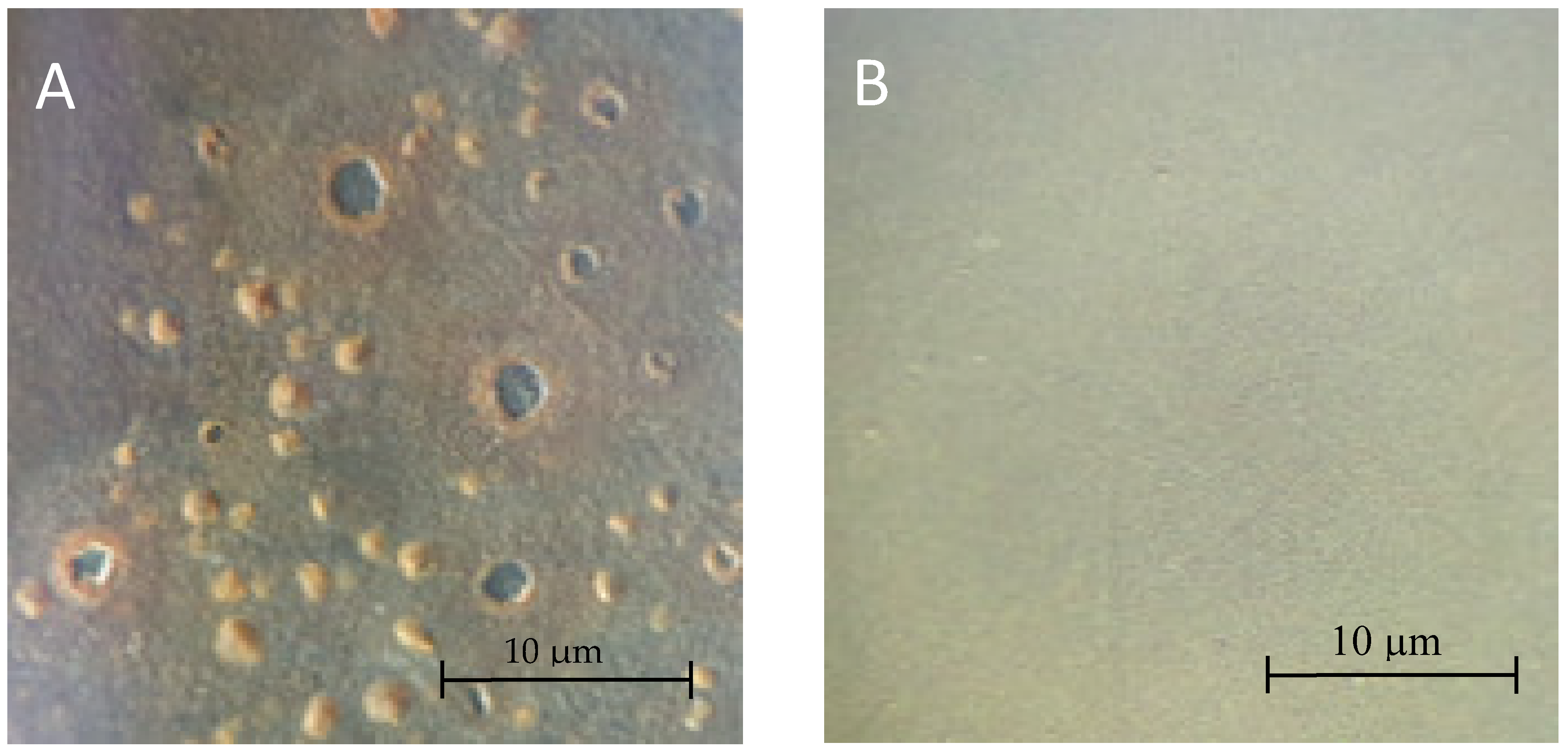
Additionally, a corrosion rapid test was performed. Uncoated and boron-coated steel samples were placed in 25 wt.% saturated aqueous NaCl solution and exposed at 70 °C for 200 h. We tested 2 samples without coatings and 10 samples with deposited boron coatings, including those treated with a pulsed electron beam. Uncoated samples bore traces of pitting corrosion, distinctly seen in
Figure 9a. Signs of corrosion were not noticeable on the surface of all the boron-coated samples. As an example, we include here pictures of the sample surface with boron coating treated with a pulsed electron beam (regime 2) and the sample kept in the solution. This verifies the high corrosion resistance of boron coatings and the absence of slits and cracks in them.

