1. Introduction
The era of artificial intelligence and big data is introducing new workloads which operate on huge datasets. A clear example is found in machine learning (ML) and especially neural-network based techniques, which are commonly applied as a solution to find patterns and interpret large amounts of data. Despite the increasing popularity of ML algorithms, there are several challenges to efficiently implement and execute neural networks on conventional processing units based on the von-Neumann compute-centric architecture [
1] such as CPUs and GPUs. The main performance and energy bottleneck of traditional architectures is the memory hierarchy due to the huge number of inputs, weights, and partial outputs, resulting in numerous data movements which incur in higher energy consumption than the operations [
2,
3]. Thus, researchers are exploring novel hardware architectures to accelerate these algorithms by moving most of the computations “in/near-memory” and, hence, reduce the data movements as much as possible. In summary, modern applications based on machine learning are very data-intensive and demand a high level of parallelism and memory bandwidth [
4]. To address these issues, some recent works have proposed near-data processing accelerators for neural networks with the promise to break the memory wall.
Deep learning has transformed how smart devices interpret and respond to many different types of information/data, as well as the way in which we interact with our devices. The traditional keyboard and mouse, and even the currently popular touch-screens are being left behind in favor of more intuitive and yet sophisticated interfaces based on cognitive applications such as image, text, and speech recognition. Commercial examples of such applications include Virtual Personal Assistants (VPA) [
5,
6,
7] such as Google’s Assistant, Apple’s Siri, Microsoft’s Cortana, and Amazon’s Alexa. VPAs are meant to interact with an end user in a natural way (i.e., voice, text, or images), to answer questions, follow a conversation, and accomplish different tasks. These mobile applications are used on a daily basis by millions of people and are powered by efficient deep learning models. Nowadays, deep learning, and machine learning in general, has expanded its use cases and can be found not only in most of our daily life devices but also in our cities and environment, despite us not being fully aware of it. Examples range from simple classification and perceptual tasks to control algorithms for autonomous systems [
8] (ranging from home robots to drones and cars) or medical health care systems [
9] (e.g., medical diagnosis or drug discovery and development). Moreover, we are witnessing how even mature system components and algorithms can have their performance and functionality improved by deep learning techniques. For example, computer architecture researchers are exploring the integration of neural networks for branch prediction [
10], and also in computer system areas such as network protocols, data compression, or encryption.
Deep Neural Networks (DNNs) have proven to be the most effective machine learning solution for a broad range of classification and decision-making problems such as speech recognition [
11], image processing [
12], or machine translation [
13].
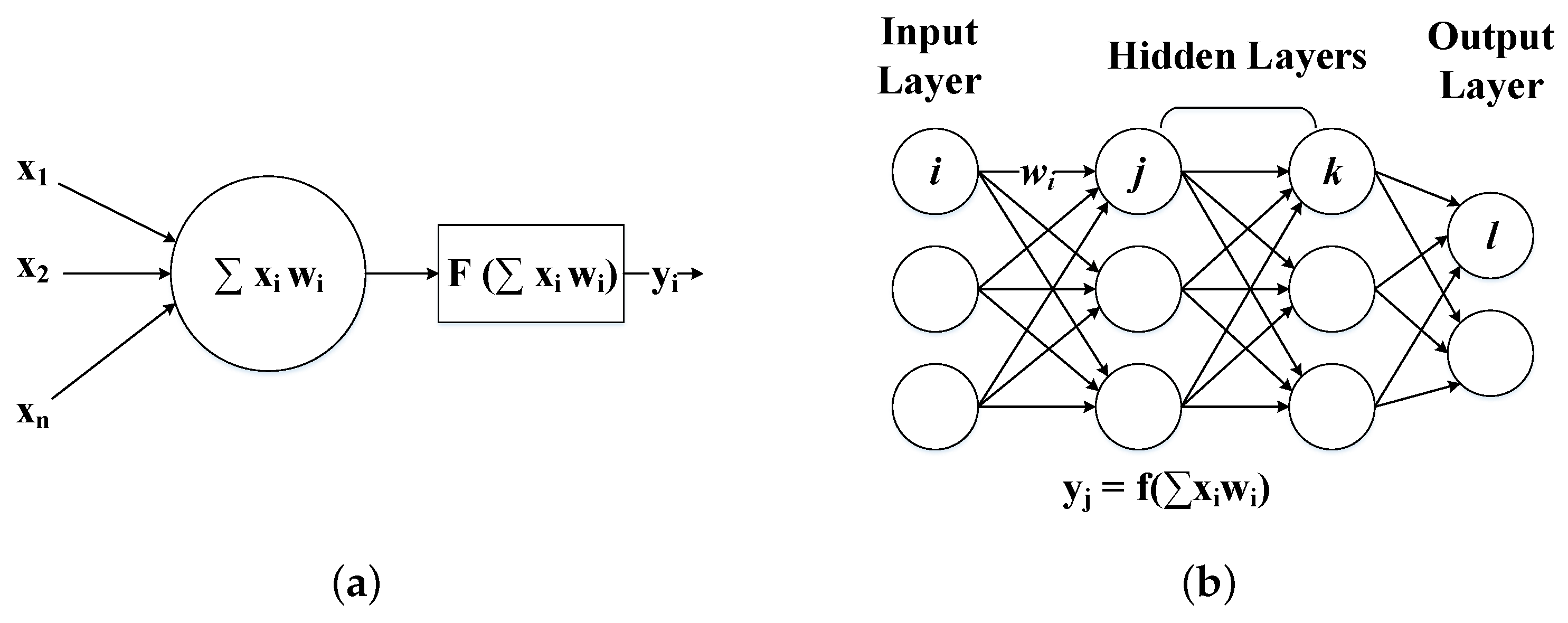
Figure 1a,b show an example of an artificial neuron and a DNN with its corresponding computations. DNNs are composed of a number of hidden layers between the input and output layers, forming feed-forward networks, which means that the outputs of one layer become the inputs of the next layer in the model, or recurrent networks, in which the output of a neuron can be the input of neurons in the same or previous layers. Each layer consists of a set of neurons interconnected with the neurons of adjacent layers according to the degree of relevance among them. The output of each neuron in a given layer is computed as an activation function of a weighted (
W) sum of its inputs (
X) as shown by Equation (
1). The main computational cost of a DNN comes from the weighted sum of inputs of each neuron and layer as the activation functions can be mapped and implemented using look-up tables. Note that although the inputs of a layer depend on the outputs of the previous layer, there is still a high level of parallelism within each layer.
Modern DNNs, such as AlexNet [
14] and GoogleNet [
15], are composed of hundreds of layers where a single execution can demand the evaluation of millions of model parameters (i.e., weights). In consequence, DNN models tend to be huge, their size ranges from tens to hundreds of megabytes, or even gigabytes, and computing the weighted sum of inputs for each neuron of a given layer requires a large number of data movements between the different levels of the memory hierarchy and the processing units. Furthermore, in order to be able to exploit the high level of parallelism of the DNN layers, a high memory bandwidth is required to provide the necessary data to feed multiple processing units. This enormous traffic in the memory hierarchy represents a great portion of energy consumption for any given device and, together with the high memory storage and memory bandwidth requirements, heavily constrains the efficiency of the compute-centric architectures.
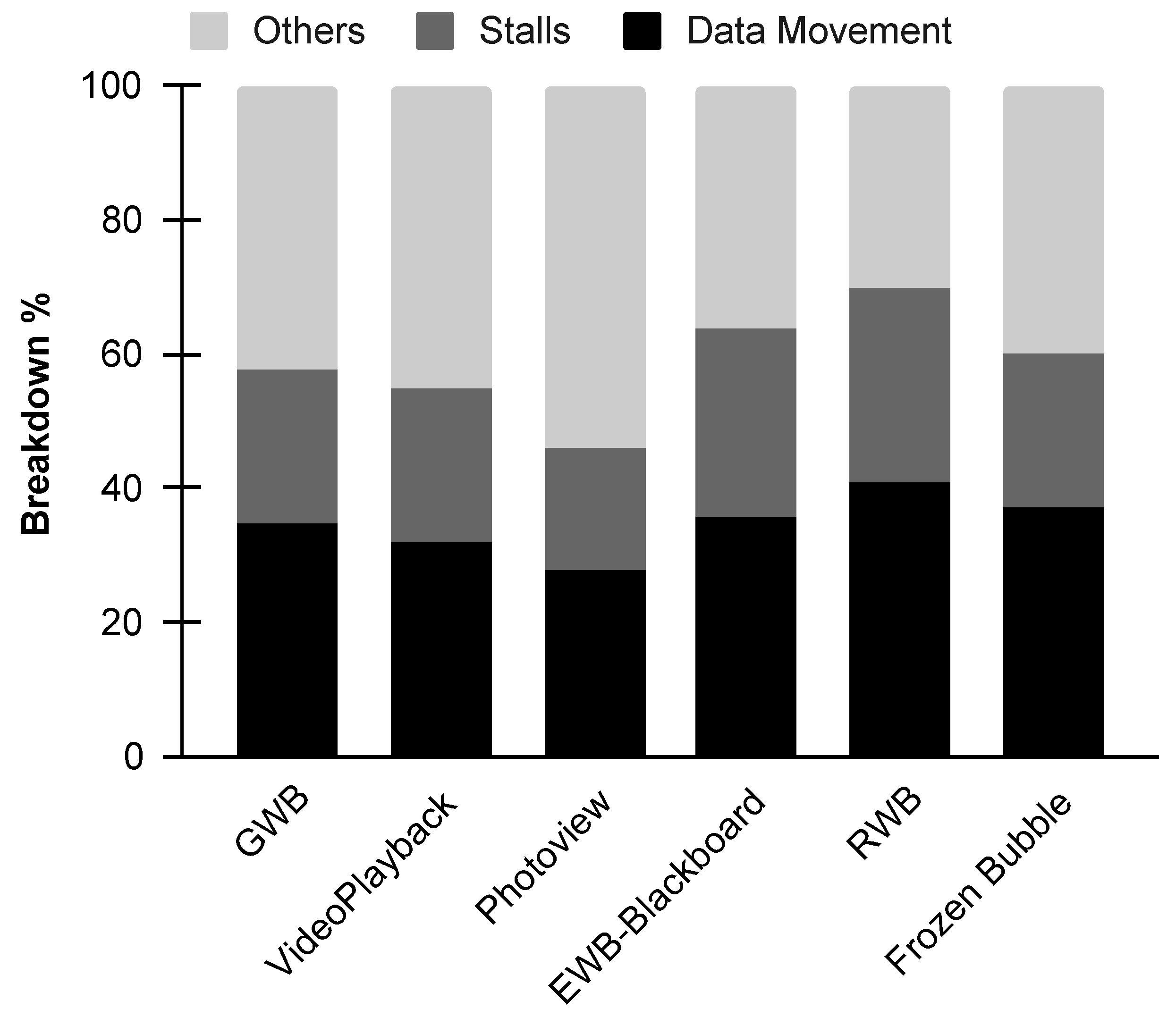
The study in [
2] quantified the energy cost of data movement for emerging smartphone workloads on mobile platforms. To illustrate the high energy cost of the memory traffic,
Figure 2 shows an example of the total energy breakdown for different mobile workloads, where Data Movement considers the energy cost of moving data between different levels of the memory hierarchy, Stalls indicate the energy consumption during stall cycles, and the rest is represented as Others. This analysis shows that, on average,
of the total device’s energy is spent on moving data from one level of the memory hierarchy to another. A similar study on a 28 nm nVidia chip [
16], implies that the energy consumed for performing an operation is significantly lower than the amount spent for fetching operands. Specifically, the energy cost of fetching data from local memory (SRAM) and main memory (DRAM) is 26 pJ and 16 nJ respectively, compared to 1 pJ and 20 pJ for integer and floating point operations respectively. Consequently, some recent works have focused on reducing the data movements of the memory hierarchy by proposing accelerators based on memory-centric architectures.
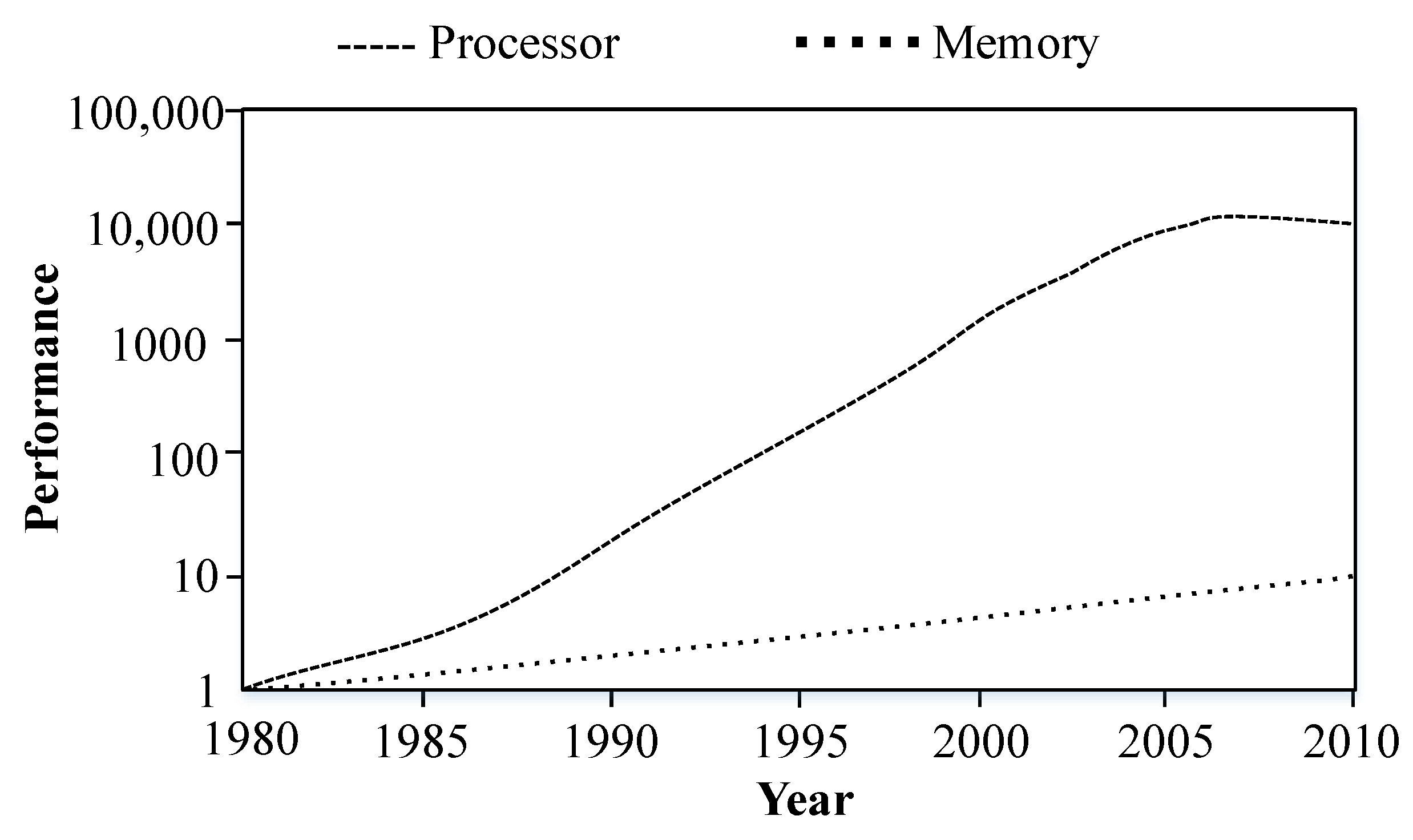
Most general-purpose computer systems and accelerators use a von-Neumann architecture, which separates the memory from the computing units. However, with the ever improving computational power of modern processing units, hardware communication fabrics struggle to advance at the same pace or even at a sufficient rate to efficiently support modern applications. It is well known that during the last 40 years the rate of improvement in microprocessor speed has exceeded the rate of improvement in DRAM memory speed. Both processor and memory performance have been improving exponentially, but the exponent for the processor is significantly higher than that of memory, in such a way that the difference between the two has also grown exponentially.
Figure 3 illustrates the performance gap over time between the memory and the processor. Due to the end of Moore’s law, the performance gap has become smaller in recent years, which has led to increased efforts to improve the memory technologies as well as the proposal of new memory-centric architectures. The “Memory Wall” [
17] problem has become the main bottleneck of data-centric applications, as large amounts of data must be moved between the memory and the processing units, generating a large volume of communication traffic in bandwidth-limited systems [
18]. DNNs are particularly susceptible to hitting the memory wall due to their large data demands and, hence, it has become one of the major challenges to be solved in order to execute ML algorithms efficiently.
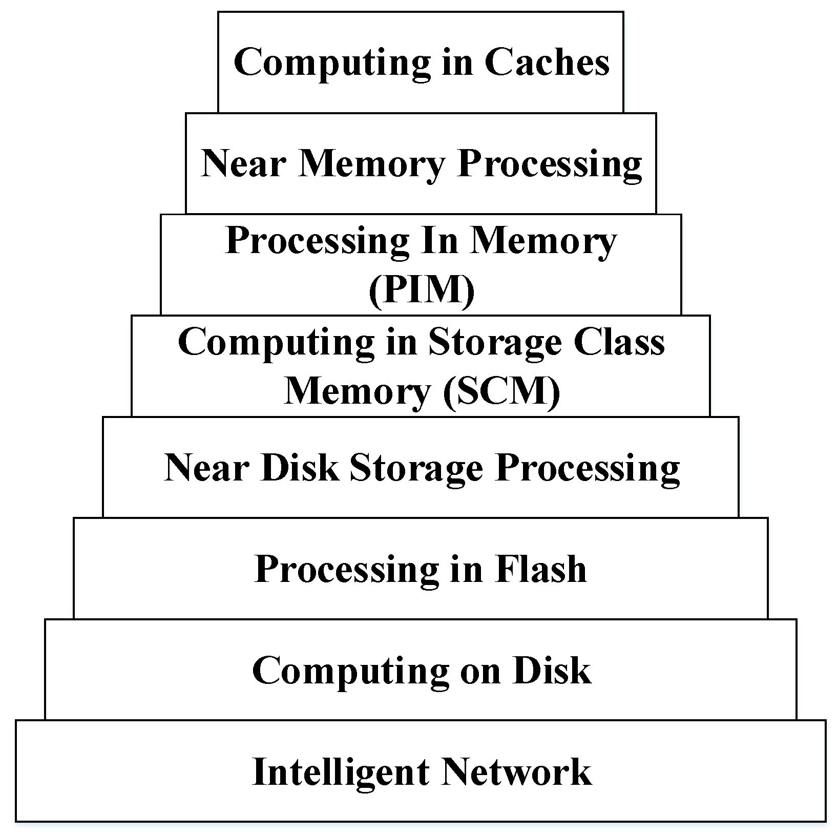
In order to overcome the problems of compute-centric architectures and alleviate the cost of communicating data between memory and the processing units, many recently proposed architectures adopt a memory-centric design based on the so-called Near-Data Processing (NDP) paradigm.
Figure 4 shows how with the adoption of the NDP approach, storage and processing units will no longer be separated, and the memory hierarchy will shift towards a processing hierarchy or a hierarchical active-data storage [
20].
NDP architectures can be further classified in two main categories. First, Near-Memory-Processing (NMP) consists of moving the processing units closer to the memory to mitigate the cost of the data movements. NMP has gained a lot of attention with the introduction of the 3D stacked memory technology, which allows the integration of logic and memory in the same chip by stacking multiple dies vertically. Popular state-of-the-art DNN accelerators such as DaDianNao [
21] and TPU [
22] also follow the NMP approach by including bigger on-chip buffers to store inputs and weights, and reuse them across processing elements to limit the data transfers. On the other hand, Processing-In-Memory (PIM) consists in removing the necessity of moving data to the processing units by performing the computations inside the memory [
23,
24,
25]. The PIM approach is commonly implemented by exploiting the analog characteristics of emerging Non-Volatile Memories (NVM) such as ReRAM crossbars, but not only NVMs can be used to perform computations [
26,
27], but also commodity memory technologies such as DRAMs and SRAMs have demonstrated the ability to perform logic operations with small changes to the memory array peripherals. Both NMP and PIM address the memory wall issue by spatially merging compute and storage units, drastically reducing the number of data transfers as well as their cost.
In this paper, we present a survey of near-data processing architectures for machine learning, and DNNs in particular. To achieve a balance between brevity and breadth, we only include state-of-the-art techniques implemented using commodity memories, 3D stacked memories based on DRAM, and ReRAM crossbars, although other emerging memories also provide NDP capabilities. We focus on describing the qualitative insights without generally including quantitative results, and paying special attention to the architectural and system-level techniques. This paper is expected to be useful for computer architecture researchers and practitioners.
The rest of the paper is organized as follows.
Section 2 provides some background information on modern DNNs, commodity memories and emerging memory technologies.
Section 3 reviews the state-of-the-art NDP architectures for data-centric applications such as neural networks, and discusses the main advantages and disadvantages of the different proposals. Finally,
Section 4 concludes this paper with a discussion of future perspectives.
2. Background
In the following subsections we review some terminology and concepts that may be helpful throughout this survey. First, we give a general description of deep neural networks (DNNs), including the main DNN categories and their different types of layers. Next, we review some fundamental concepts about conventional memory technologies such as DRAM and SRAM, which have proven to be capable of doing computations inside the memory arrays. Finally, we discuss new memory technologies such as ReRAM crossbars and 3D-stacked memories, which offer more opportunities, over commodity memory technologies, to implement a highly efficient DNN accelerator in terms of both performance and energy consumption.
2.1. Deep Neural Networks (DNNs)
Deep learning [
28,
29] is a set of algorithms that is part of a larger family of machine learning methods based on artificial neural networks and data representation techniques that allow to learn and interpret features of large datasets. DNNs are a type of deep learning model that aims to mimic the human brain functionalities based on a very simple artificial neuron that performs a nonlinear function, also known as activation function, on a weighted sum of the inputs. As discussed in
Section 1, these artificial neurons are arranged into multiple layers. The term “deep” refers to the use of a large number of layers, which results in more accurate models that capture complex patterns and concepts. DNNs are typically used as classifiers in order to identify which class the current input belongs to, so the last layer of the network often performs a softmax function that generates a probability distribution over a list of potential classes.
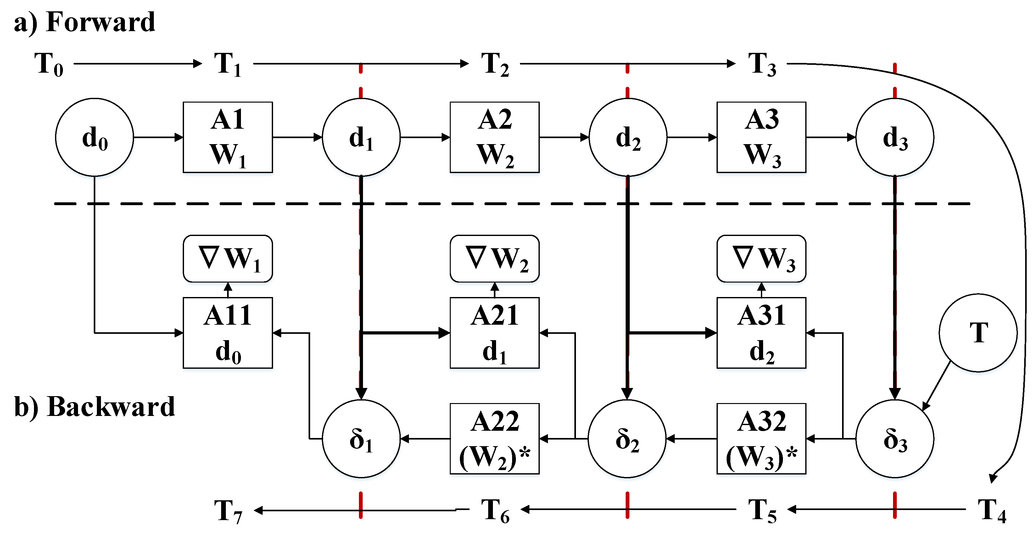
DNN’s operation has two phases, training (or learning) and inference (or prediction), which refer to the DNN model construction and use, respectively. The training procedure determines the weights and parameters of a DNN, adjusting them repeatedly until the DNN achieves the desired accuracy. During training, a large set of examples, with its corresponding labels indicating the correct classification, is used to execute the DNN’s forward pass and measure the error against the correct labels. Then, the error is used in the DNN’s backward pass to update the weights. On the other hand, inference uses the DNN model developed during the training phase to make predictions on unseen data. Although the DNN training is complex and computationally expensive, it is usually performed only once per model, and then the learned weights are used in inference as many times as it is required to classify new input data. On the other hand, DNN inference has strict latency and/or energy constraints and, hence, many research works focus on improving the execution of the inference phase. Nevertheless, a recent line of research with increasing popularity aims to propose efficient DNN accelerators for both phases.
DNNs can be classified in three main categories. Multi-Layer Perceptrons (MLP) [
30] consist of multiple Fully-Connected (FC) layers in which every input neuron is connected, via synapses with particular weights, to every output neuron. Convolutional Neural Networks (CNN) [
31] are composed of multiple convolutional layers to extract features, usually followed by one or several FC layers to perform the final classification. CNNs have proven to be particularly efficient for image and video processing. Finally, Recurrent Neural Networks (RNN) [
32] consist of multiple layers of cells with feedback connections. RNN cells store information from past executions to improve the accuracy of future predictions, where cells consist of multiple single-layer FC networks commonly referred as gates. Each type of DNN is especially effective for a specific subset of cognitive applications. Moreover, for each application, each DNN has a different composition of layers with specific operations. The fully-connected (FC), convolutional, and recurrent layers take up the bulk of the computations in most DNNs. Other types of layers performing pooling, normalization, or activation functions are also common in modern DNNs. However, these other layers have no synaptic weights and represent a very low percentage of the DNN execution time. In consequence, state-of-the-art DNN accelerators focus on optimizing the execution of FC and convolutional layers.
2.2. Conventional Memory Technologies
Conventional memory technologies are widely used in the memory hierarchy of many current systems. DRAM is commonly employed for the main memory of most computer systems while SRAM is used to implement CPU caches and register files, as well as small buffers for different components. Both DRAM and SRAM are considered commodity memories, and a popular line of research tries to take advantage of the widespread use of these memories to perform near data processing by proposing minor changes to the memory chip circuitry, as we will describe later in
Section 3.1.
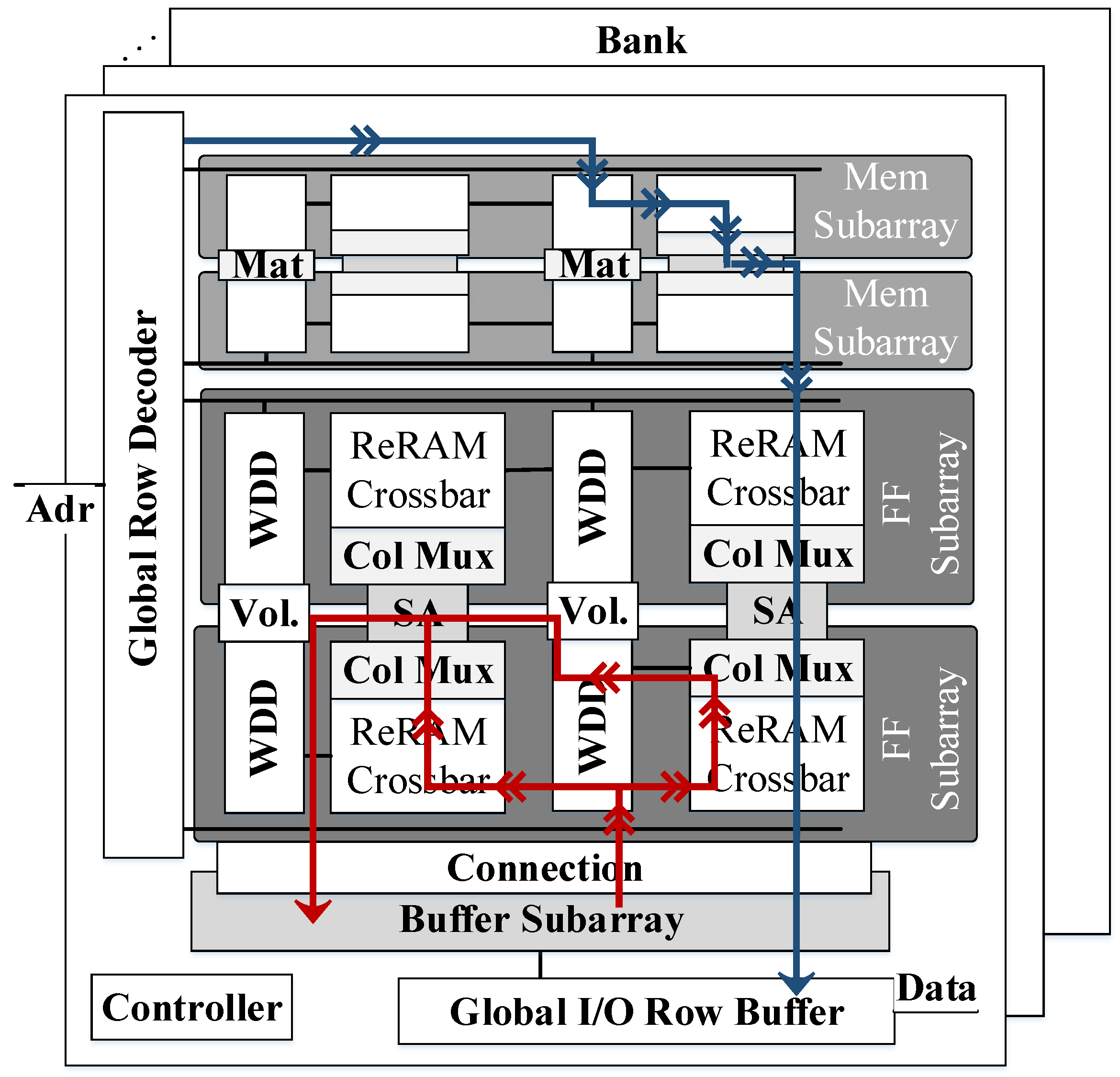
A DRAM or SRAM chip is commonly divided into multiple memory banks connected to a global bus. Each bank consists of multiple memory arrays containing the DRAM/SRAM cells.
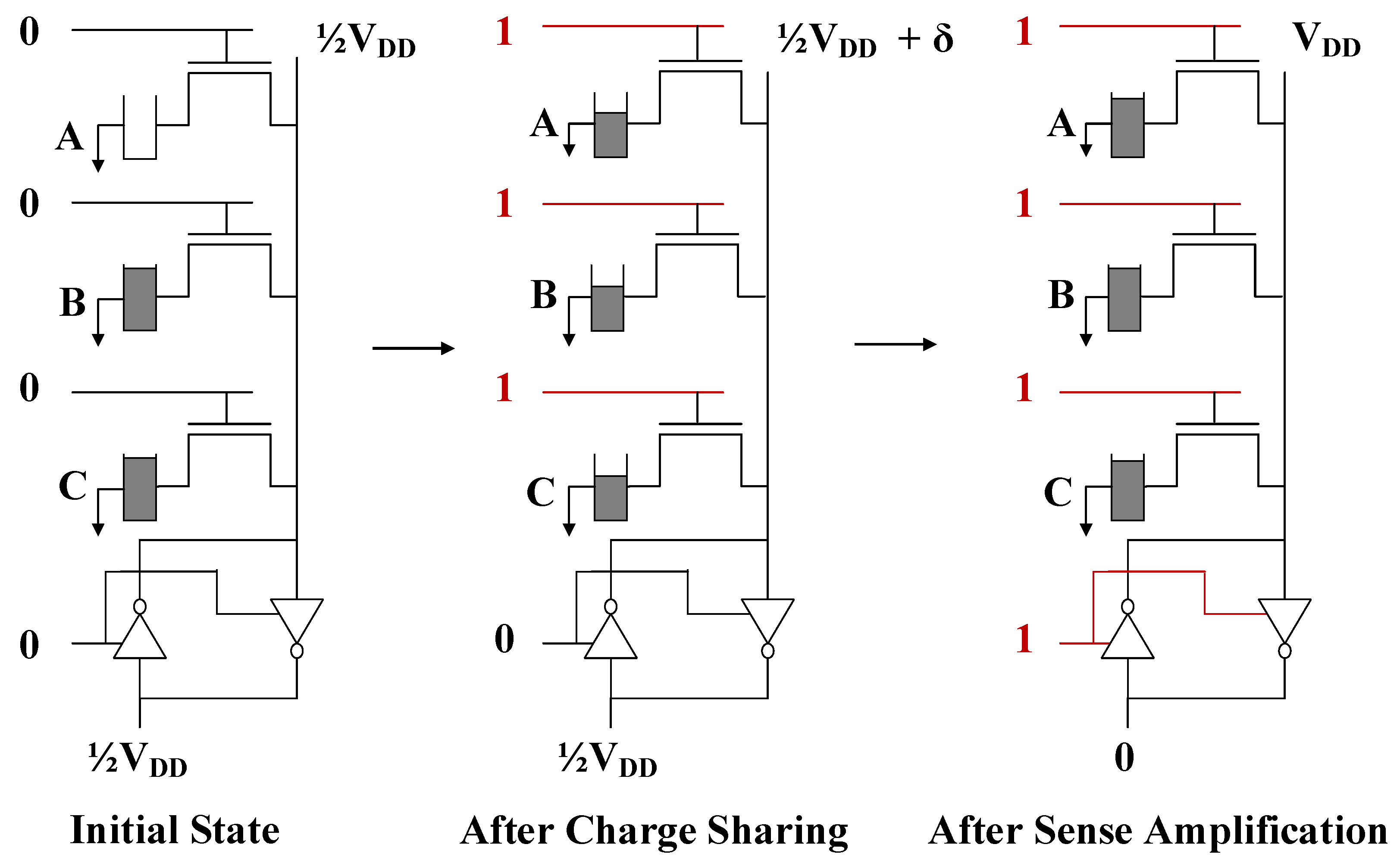
Figure 5 shows an example of a typical 2D organization (i.e., memory array) of a DRAM or SRAM chip. The cells of a given row of the memory array are connected to a Word-Line (WL) while the cells in the same column share the same Bit-Line (BL). The read and write operations are performed by activating the WL of the corresponding row of the array, and exploiting the charge sharing effect of the bitlines. Among the peripherals of the memory array, the decoders are required to map and translate the addresses of the memory accesses to specific rows and columns of the array, while the sense amplifiers in the column circuitry detect small changes in the voltage of the bitlines and amplify the swing over a reference voltage to help to perform the read and write operations.
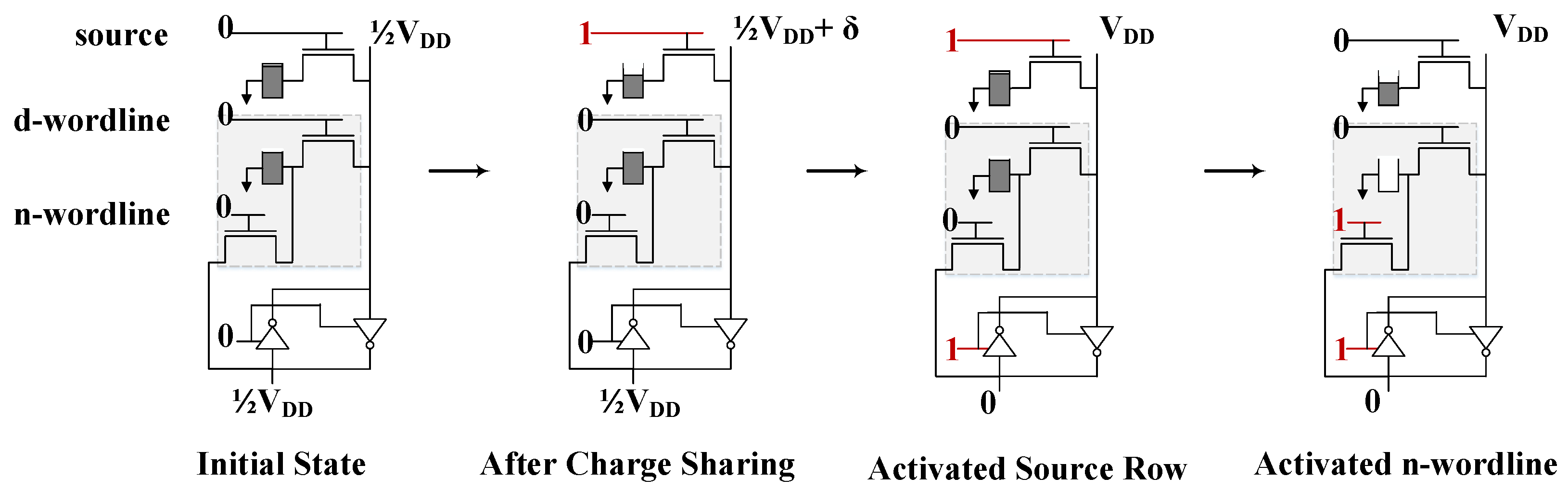
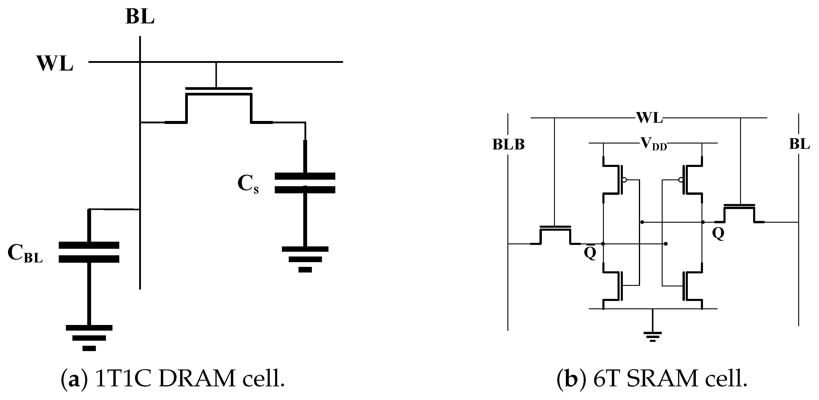
A DRAM cell stores one bit of information using a capacitor and an access transistor as shown in
Figure 6a, which is known as the 1T1C cell design. During the read operation, all the bitlines of the array are pre-charged equally to
using the peripheral drivers. Then, the corresponding WL of the row to be read is activated. Due to the charge sharing effect, the capacitance of the bitlines start to lose (if stored value is 0) or gain charge (if 1 is stored) changing the pre-charged voltages by a small amount, and destroying the values stored in the cells of the row. The small voltage swing in each of the bitlines is sensed and amplified to a stable state by the sense amplifiers and, hence, the value of each bitline is converted to a strong one (i.e.,
) or zero accordingly. Finally, as the WL is still active and connecting the capacitor of each cell of the row to the corresponding BL, the capacitors are fully charged (or discharged), restoring their original value. Similarly, to perform a write operation in a row of cells, the bitlines are pre-charged to
(to store 1) or 0 (to store 0), and the corresponding WL is activated. As the sense amplifiers hold the voltage of each bitline at a stable state, the capacitor of each cell will continue to charge (or discharge) until the pre-stored value is overwritten with the new value.
SRAM cells store bits of data and their negated versions using four transistors in the form of cross-coupled inverters. In addition, two more transistors are employed to control the access to the bitlines.
Figure 6b shows a typical SRAM 6T cell design. On a read request, both bitlines,
and
, are pre-charged to
. Then, when the WL of a cell is activated, one of the bitlines starts to discharge, that is,
if the stored value is zero or
otherwise. The read operation has the potential to change the stored value and, hence, the size of the transistors must be chosen carefully so that the original value does not flip. To write a new value in a 6T cell,
and
are driven to high and low to store a one, or the other way around to store a zero. Then, the WL is activated, and the bitlines overpower the cell with the new value.
DRAM cells are small as they are typically composed of one transistor and one capacitor, which provides higher density over SRAM memories. Despite the higher capacity of DRAMs, the 1T1C cells are not ideal due to the high leakage of the capacitor’s charge, which might lead to losing the stored values after some time. In consequence, DRAM cells require additional circuitry to perform regular refreshes of the cell values, which has a negative impact on DRAM performance. On the other hand, SRAM is faster than DRAM and does not need any refresh circuitry. However, the 6T cells are large, resulting in lower density and higher cost. Therefore, DRAM is preferred over SRAM for main memory due to its higher capacity and lower cost, while SRAM is employed for caches and small buffers due to its higher performance.
2.3. Resistive Random Access Memory (ReRAM)
In 1971, Leon Chua [
33] theorized about the existence of a fourth passive electrical component that he referred to as the “memristor” (or memory resistor), complementing the quartet of fundamental electrical components together with the resistor, the inductor, and the capacitor. In 2008, a team at HP Labs managed to develop the first physical memristor switch [
34], and later on started the prototyping of ReRAM memories using them.
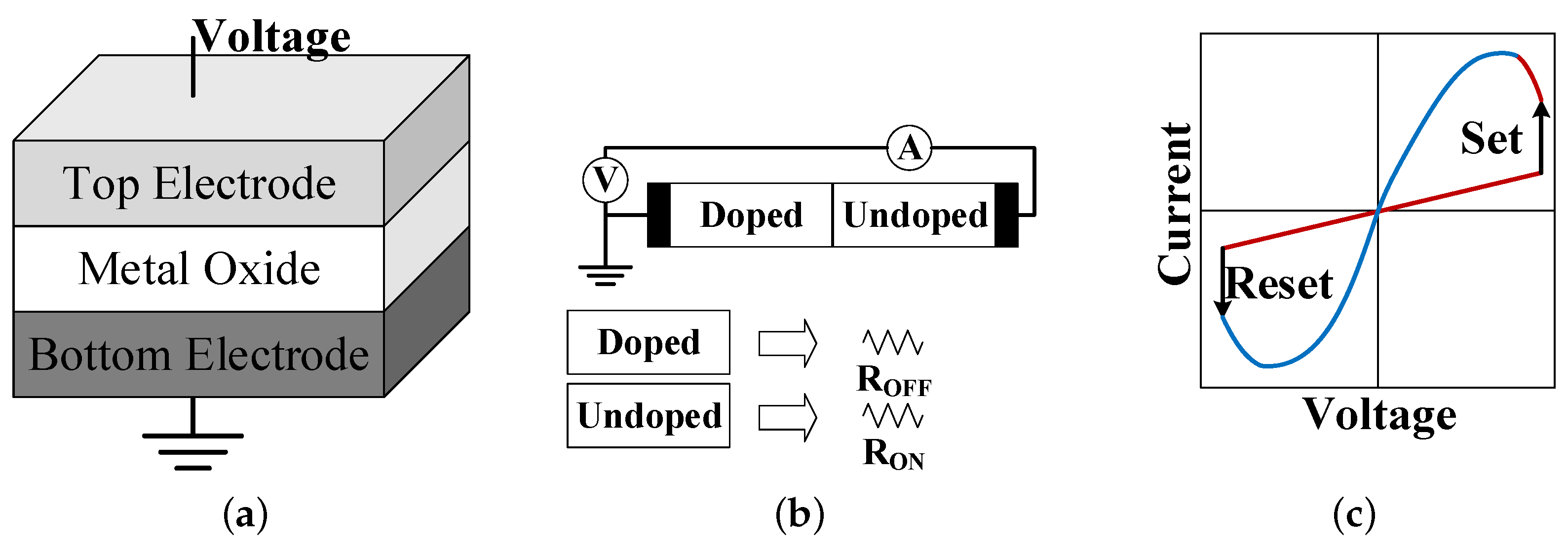
A memristor is a non-linear two-terminal electrical component with a layer of a resistive switching material sandwiched between the top and bottom electrodes as shown in
Figure 7a. The resistive switching material layer consists of two regions, “doped” and “undoped”, with low (
) and high (
) resistances, respectively, which is equivalent to connecting two resistors in series as shown in
Figure 7b. The memristor’s electrical resistance depends on the history of current that had previously flowed through the device, that is, the amount of electric charge flowing through the memristor device changes the length of the two regions based on the direction of the current and, as a result, the total resistance varies. The memristor device remembers its most recent resistance after turning off the power supply achieving the so-called non-volatility property [
35].
Figure 7c shows the I–V curve of a typical bipolar ReRAM cell. By applying an external voltage across a memristor, a ReRAM cell can be switched between a high resistance state (HRS) and a low resistance state (LRS), which are used to represent the logic “0” and “1”, respectively. Switching a cell from HRS (logic “0”) to LRS (logic “1”) is a SET operation, and the reverse process is a RESET operation. To SET the cell, a positive voltage that can generate sufficient write current is required, while to RESET the cell, a negative voltage with a proper magnitude is necessary. In addition, ReRAM cells can store more than one bit of information by employing various resistance levels, which can be realized by changing the resistance of a ReRAM cell gradually with finer write control. This multi-level cell (MLC) characteristic makes the ReRAM memories suitable for storing a large amount of DNN weights.
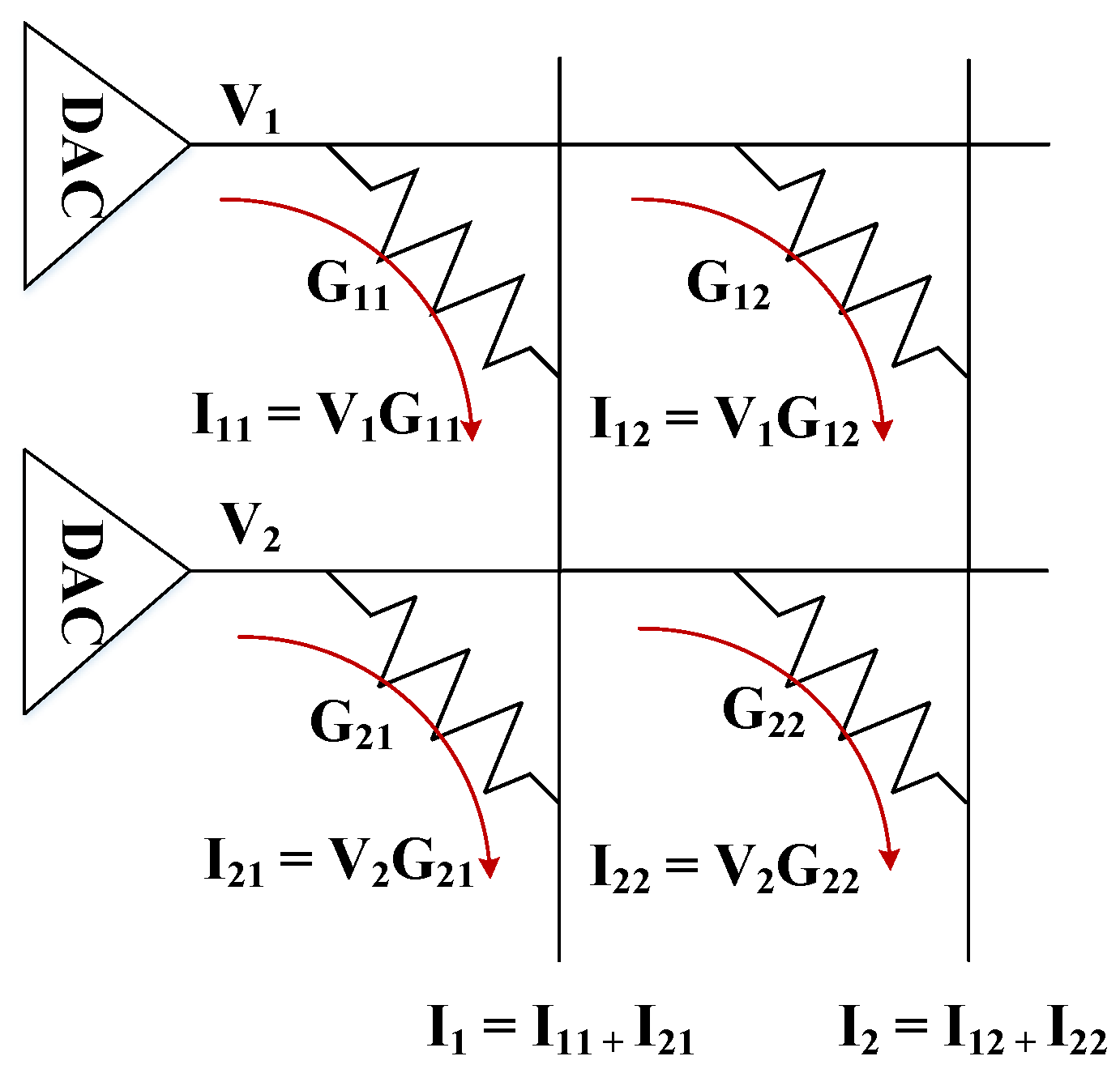
Recent works have demonstrated the use of ReRAM devices to perform dot-product computations which, as described previously, are common in many DNN layers.
Figure 8 shows an example of an analog MAC operation, and a MVM using a ReRAM crossbar. Similar to the conventional memory technologies, each BL of a ReRAM memory array connects to each WL through a ReRAM cell, which usually consists of a single memristor with an access transistor, also known as the 1T1R cell design. Applying a voltage
to a ReRAM cell with resistance
results in a current of
passing from the cell to the bitline, as per Ohm’s law, where
. Then, from Kirchoff’s law, the total current from the bitline is the sum of currents generated through all the cells sharing the same bitline, that is, the total current (
I) is the dot-product of input voltages at each row (
V) and cell conductances (
G) in a column as shown by Equation (
2). This can be used to implement a DNN in an efficient manner. In this case, the synaptic weights of neurons are encoded as conductances of the ReRAM cells. Then, the total current of a BL is used to compute the output of a neuron in a given layer. Note that the dot-products are applied massively in parallel performing a MVM in a single time step.
Implementing DNN accelerators using ReRAM devices is quite effective, as ReRAM provides high capacity to store the weights, low latency to access them, and high performance PIM capabilities to perform the dot-products. In addition, as the leakage current of memristors is significantly lower than DRAM/SRAM cells, the energy efficiency can be highly improved. Furthermore, ReRAM devices can also be used for implementing bitwise operations and search operations which can be useful to implement different DNN layers.
Section 3.3 describes state-of-the-art NDP accelerators for DNNs based on ReRAM architectures.
Despite the numerous benefits, the use of ReRAM devices also present several challenges [
37]:
Challenges in Achieving High Performance: Despite the low read latency of ReRAM, changing a memristor’s resistance value requires a high and long enough voltage, which incurs in high write latency and energy consumption compared to SRAM. Consequently, the weights of a neural network are usually pre-stored in multiple ReRAM crossbars, and are reused across multiple executions to avoid writes as much as possible. Furthermore, ReRAM is not suitable for DNN training due to the high number of writes that are required to update the weights. In addition, the non-ideal characteristics and limitations of ReRAM, such as process variations, can reduce their performance even further.
Challenges in Analog/Digital Domain: The dot-product computations within a ReRAM crossbar require input voltages in the wordlines and produce output currents in the bitlines, thus operating in the analog domain. However, not all components in a DNN accelerator work in the analog domain, either due to the impossibility of implementing the operations of some layers in analog domain, or as some operations are executed much faster using digital components and cannot be accelerated with the use of ReRAM. Therefore, to perform computations using ReRAM, the digital inputs must be converted to analog voltages, and the analog outputs are converted back to digital, hence requiring the use of DACs and ADCs and incurring high power consumption and area overheads, which limits the scalability of ReRAM crossbars. For example, ISAAC’s ADCs account for 58% of power and 31% of area for a given tile of the accelerator [
38]. In addition, the precision of the analog computations, and the overall accuracy of the DNN model, may be affected by the signal degradation of using DACs/ADCs, external noise signals, or non-zero wire resistance, among other sources of errors.
Reliability Challenges of ReRAM: Most ReRAM reliability issues come from the high defect rate and process variations (PV) that happen during fabrication. The faults are considered soft when the resistance of the memristor can still be changed but the result is different from the expected value, or hard when the memristor becomes stuck at a given resistance state. The hard faults may happen, not only due to PV, but also due to the ReRAM’s limited write endurance, which is another important obstacle for its general applicability. To mitigate these issues, redundancy-based techniques can be used; however, they incur significant complexity and area overheads.
2.4. 3D-Stacked Memory
3D stacking aids the design of future computing systems by allowing for wider buses and faster on-chip memories, and by enabling the composition of heterogeneous dies, built using different process technologies, within a single package. High density 3D memory is a promising emerging technology for the memory system of DNN accelerators. It consists of stacking multiple memory dies on top of each other, which increases the memory capacity and bandwidth compared to 2D memory, and also reduces the access latency due to the shorter on-chip wiring interconnection [
39]. These aspects can lead to an overall improvement in performance and power efficiency. Compared with the conventional 2D DRAM, 3D memory provides an order of magnitude higher bandwidth (160 to 250 GBps) [
40] with up to 5× better energy efficiency and, hence, 3D memory is an excellent option for meeting the high throughput, low energy requirements of scalable DNN accelerators.
The 3D memory dies are commonly based on DRAM, but the integration of other memory technologies is being actively researched with very promising results. For example, the 3D XPoint developed by Intel and Micron is a commercial Non-Volatile Memory (NVM) based on ReRAM. On the other hand, recent advances in low-capacitance through-silicon vias (TSVs) technology have enabled 3D memory that includes a few DRAM dies on top of a logic chip. Although there are numerous implementations of 3D-stacked memory technologies, the Hybrid Memory Cube (HMC) is the preferred choice for most DNN accelerator proposals [
41,
42]. There are several works that place multiple arrays of NN processing elements on the logic layer of an HMC to improve performance and power efficiency.
Section 3.2 describes state-of-the-art NDP accelerators for DNNs based on DRAM HMC architectures.
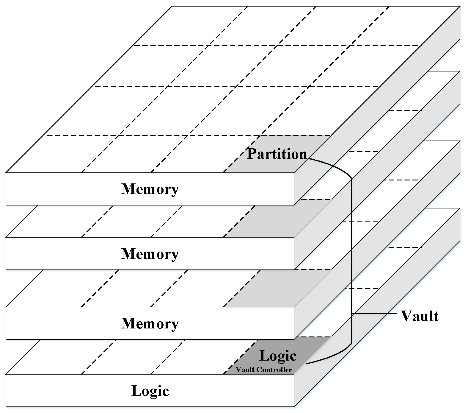
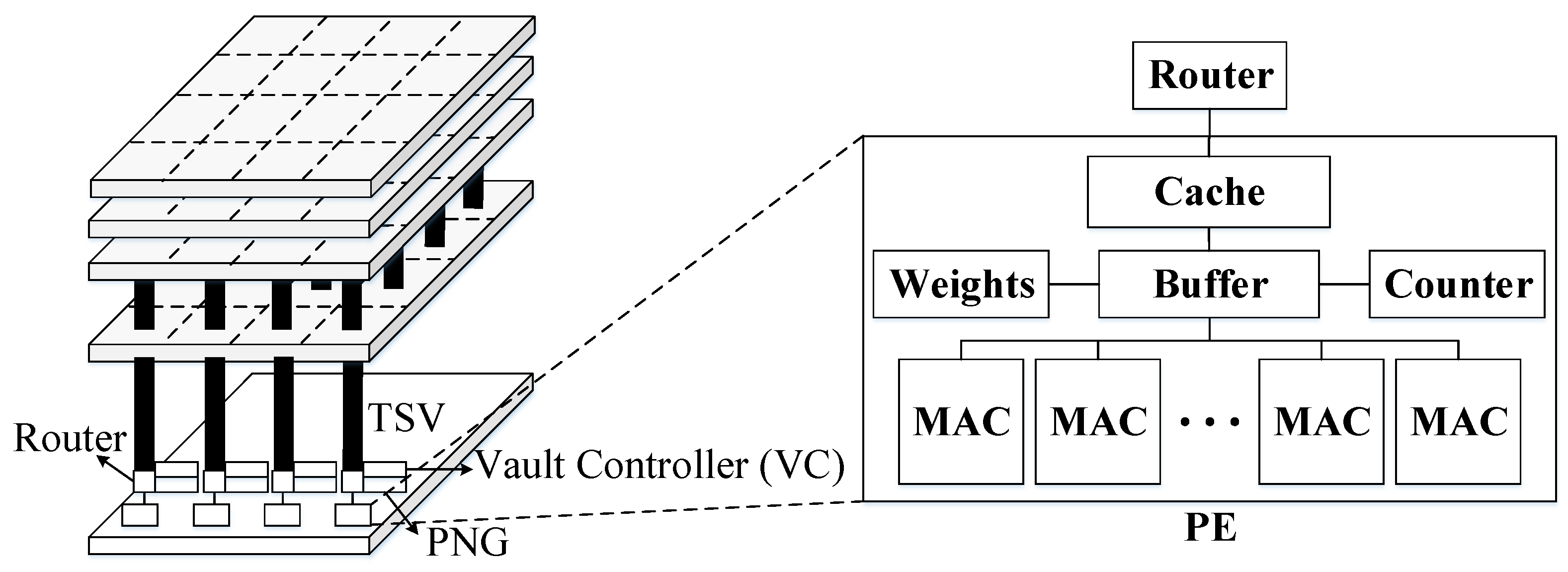
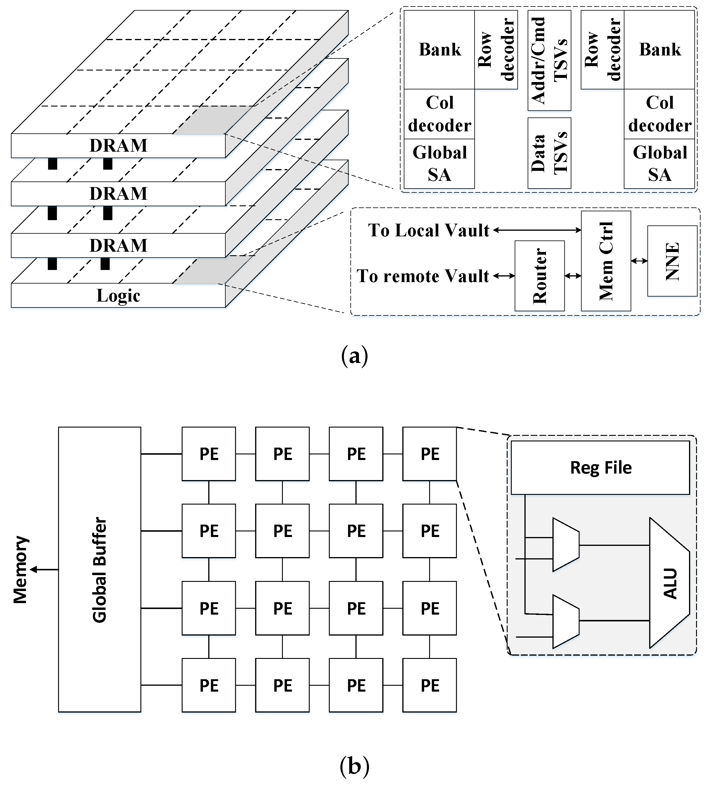
The Hybrid Memory Cube (HMC) is designed for high performance data-centric applications.
Figure 9 shows a high-level diagram of an HMC, which is usually composed of multiple vertically stacked DRAM dies with a single logic layer at the bottom. The different layers are interconnected using thousands of TSVs to attain the much desired high memory bandwidth, and each DRAM die is divided into multiple partitions in a 2D grid where the corresponding partitions on the vertical direction form a single vault. In addition, the large number of TSVs can be organized into multiple independently-operated channels that exploit memory level parallelism, that is, one channel per vault where each vault has an independent vault controller on the logic die and, thus, multiple partitions in the DRAM die can be accessed simultaneously. The HMC provides highly parallel access to the memory which is well suited to the highly parallel architecture of the DNN accelerators [
43]. The logic and memory dies can be fabricated in different process technology nodes. However, the area of the logic die relative to the memory dies is constrained by the package, and power dissipation is limited by much tighter thermal constraints.
To fully exploit the benefits of 3D-stacked memory, there are several challenges to address. First, given the characteristics of 3D memory, it may be worth revisiting the design of on-chip buffers in the logic die, as the lower latency and energy cost of the accesses to main memory allow for smaller and faster on-chip buffers with different use cases. Second, 3D integration technology also provides opportunities to rethink where computations are executed, potentially moving some operations closer to the actual memory locations. Third, HMC changes the memory and computer hardware, creating a highly parallel system with multiple vertical channels and, thus, one which opens the door to new approaches for dataflow scheduling and efficient partitioning of DNN computations. Last but not least, the thermal issues for 3D stacking, as well as higher manufacturing complexity, lead to lower yield and problematic testability. Therefore, stacking multiple dies can increase the operation temperature resulting in performance degradation and, hence, proper cooling methods and better manufacturing solutions are required to extend the adoption of this technology.
To summarize, 3D-stacking is not just a solution for the memory wall but rather a key-enabler in single chip packaging, with low to medium risk involved, to accomplish a reduction in system-level power as well as form factor. HMC integrates fast logic layer and dense memory layers and allows for embedding fast processing units close to a large and high-bandwidth memory system. Furthermore, HMC offers a unique novel abstract bus interface to communicate with the CPU host, and high parallelism via the so-called independent vaults, making it a very promising solution for DNN accelerators.
4. Conclusions and Future Perspectives
Recent advances in traditional memory systems, as well as new memory technologies, have renewed interest in an old research topic (i.e., 1970 [
56]), currently known by the name of Near-Data Processing (NDP). In addition, many modern applications are data intensive and demand a high level of parallelism and memory bandwidth. While deep learning techniques, and machine learning in general, are promising solutions to a broad range of applications, the characteristics of conventional memories and processors limits their potential. Addressing these challenges requires fundamental breakthroughs in memory and computer architectures. In this paper, we present a survey of techniques for designing DNN accelerators with NDP architectures. We described the key insights of different recent works and organized the works in several categories based on the memory technology employed to highlight their similarities and differences. Finally, in this section, we conclude the paper with a discussion of future work.
Based on the observation that DRAM/SRAM arrays can simultaneously activate multiple rows to perform bitwsise operations, many prior works focus on adding PIM capabilities to commodity memories with minor changes, so that the main structure and interface to communicate memory and CPU/GPU systems remains the same. Future works can remove the need to keep the architectural structure of traditional memory systems with custom accelerators. ASICs are an interesting solution, as they are more flexible and offer the opportunity to combine different memory technologies, conventional and emerging, with PIM capabilities to provide a computer system optimized for data-centric applications. For example, Ambit could be implemented in an HMC, and be further extended and improved to exploit this new memory technology. Moreover, most works based on traditional memory systems only include computation capabilities in a specific level of the memory hierarchy, such as the LLC or main memory, but multiple levels of the hierarchy could be used combined with novel dataflows.
In another line of research, Ambit and Neural Cache effectively exploit the bandwidth of typical DRAM and SRAM arrays, respectively, and the parallelism of multiple arrays, but only perform computations between two rows of a given array. While two rows may already offer a high level of parallelism, it can be a major drawback compared to ReRAM crossbars that can operate using the entire array. Further research could be undertaken to exploit the analog operation of SRAM/DRAM arrays to increase the level of parallelism, which may require the use of modified memory cells and peripherals. Following this direction, Neural Cache includes extra logic in the sense amplifiers of SRAM arrays to perform complex operations, and Ambit employs a row of 2T1C cells for the DRAM bitwise NOT operation. Other new memory arrays with additional logic in the peripherals and/or a mix of different cells to perform faster operations could be investigated. Furthermore, new data layouts could be explored to facilitate the interaction between bitlines. Although additional circuitry may be expensive and reduce the memory density, ASICs can be flexible enough in terms of storage capacity to overcome the overheads.
In addition, it is critical to design efficient and reliable PIM DRAM/SRAM arrays taking into account not only the negative effects of process variations, but also aging and soft errors.
On the other hand, Bit-Prudent extends Neural Cache with support for sparse and low-precision models, but they only consider a structured channel pruning for CNNs and binary/ternary networks. New pruning methods and dynamic precision approaches can be studied and evaluated in combination with novel hardware changes to support these models in NDP architectures based on commodity memory. Additionally, given the limitations of CMOS technology, the use of new emerging memory technologies, such as HMC or ReRAM, could also be interesting for these designs.
Most works based on 3D-stacked memory with HMCs perform the majority of the computations in the logic die. In contrast, TETRIS introduced some adders in the DRAM dies to perform accumulations, and although the technology process to fabricate the different layers may differ and be slower, solutions that perform more computations in the memory layers could be further investigated. Following this approach, the level of parallelism in HMCs can be increased, exploiting not only the independent vaults but also the different memory layers, which may require a better organization of the data as well as novel dataflows.
In the same line, Neurocube and TETRIS are mostly focused on CNNs, but recent DNN models, such as RNNs or Transformers, may also require new data mappings and execution schemes. In addition, these accelerators tend to work on a single NN layer at a time, but considering that there is usually enough storage capacity for the entire model, a pipelined execution of the layers could be more practical.
In addition, as there is an increasing number of applications that require the execution of multiple DNNs, efforts could be made for exploring new schedulers to support the parallel execution of multiple models, as well as potential computation reuse opportunities.
Furthermore, little research has been undertaken on DNN accelerators for both inference and training exploiting the intrinsic features of 3D-stacked memories. Similarly, sparse DNN accelerators based on HMCs have received little attention. Moreover, some of these solutions may incur in additional traffic to communicate between vaults, turning the NoC into a potential bottleneck of the system, and requiring additional improvements. On the other hand, some of the main challenges to extend the adoption of 3D-stacked memory and HMCs are the thermal and area constrains, which limit the scaling of the architectures based on this technology and, hence, proper solutions are required to relax theses restrictions.
Following a parallel line of research, most ReRAM based architectures have focused on accelerating a limited range of computations/algorithms, such as bitwise operations or MVM, which represent the majority of the DNN computations. However, not every DNN model/layer/operation can be easily integrated into every NDP accelerator. For example, the normalization layer requires operations that cannot be easily adapted and accelerated using ReRAM crossbars and, hence, it may be important to investigate novel algorithm–hardware co-designs.
In addition, the difficulty in re-programming the memristor arrays on the fly has led many prior works to propose architectures with several ReRAM crossbars to instantiate the full DNN model once, and then proceed with a pipelined execution to improve the utilization of the resources. This solution can be very effective in an HPC environment where batches of multiple inputs can be easily generated to achieve high throughput, and where the area and power constraints are not so tight. However, embedded and mobile devices have strict restrictions, so the number of crossbars must be relatively small and not able to store the full model. In consequence, solutions that increase the ReRAM write endurance or reduce the ReRAM write latency/energy can be highly attractive for power-constrained systems, enabling architectures that execute one layer at a time and perform efficient context switching. Similarly, techniques to reduce the number of write operations such as data-compression will be very effective in dealing with the write-agnostic nature of ReRAM.
Equally important, initial proposals of ReRAM based accelerators for DNNs, such as PRIME and ISAAC, incur in high energy and area overheads due to the numerous A/D conversions, whose cost is directly proportional to the ADCs/DACs resolution. The bit-serial input voltage execution reduces the DAC resolution to just one bit. However, lowering the ADC resolution may affect the final accuracy of the DNN as the outputs would be truncated. Consequently, the design of alternative methods to perform A/D conversions is crucial to reduce these overheads. Further, each ReRAM based accelerator employs a different encoding/decoding scheme for inputs and weights with its corresponding hardware. However, it is not clear how they compare against each other. For example, PipeLayer employs an integrate and fire scheme that replaces the ADCs, but a comparative evaluation is not provided.
On the other hand, follow up works have tried to reduce the use of DACs/ADCs either by operating in analog domain as much as possible to reduce the number of A/D conversions (i.e., CASCADE), or by digitizing the full design approximating most of the operations with ND-CAM searches (i.e., RAPIDNN). Still, these approaches do not solve the problem completely and/or add other problems to be solved. Therefore, further research in this direction to propose a better design may be interesting.
Compared to DNNs, less progress has been made towards implementing Spiking Neural Networks (SNNs) on ReRAM. Similarly, training acceleration has received less attention than inference acceleration, as the training phase is more computationally demanding than the inference phase. In addition, ReRAM crossbars are not well suited for DNN training due to the long writing latency of memristor arrays and the difficulty for re-programming the ReRAM crossbar on the fly. In consequence, most previous works focus on optimizing the inference phase. PipeLayer is one of the few ReRAM based accelerators supporting training. However, their training dataflow is mostly based on state-of-the-art DNN accelerators. Similar to ISAAC, PipeLayer employs a pipelined execution that requires a large number of crossbars, which may not be suitable for low power devices. In addition, it is not clear how they deal with all the ReRAM writing issues.
As the works based on 3D-stacked memory, most state-of-the-art ReRAM based accelerators do not support the execution of sparse/binary/ternary models nor dynamic precision schemes. For example, pruning methods that are more suitable to perform analog computations with ReRAM crossbars, or schemes that dynamically change the precision of the inputs benefiting from the bit-serial input voltage execution, may be interesting lines of research.
The vulnerabilities of ReRAM crossbars, such as process variations, hard faults, or resistance drift, pose a serious threat to the accuracy of in-ReRAM computations. In addition, crossbars and DACs/ADCs can be exposed to analog signal degradation or external noise sources that can further reduce the DNN model quality. Tolerating these errors is feasible only in error-resilient applications which comprise a fraction of the total applications. Consequently, advanced manufacturing processes will be even more crucial to reduce the ReRAM vulnerabilities, and future research should focus on improving the design of the accelerators to be more resilient to possible errors while maintaining the performance and energy efficiency.
In general, most existing NDP architectures for DNNs employ HMCs with DRAM dies or ReRAM crossbars. A comparative evaluation of other high density 3D stack memory technologies such as Wide I/O and HBM would be also interesting, as well as combining 3D stack architectures with NVMs such as PCM and STT. Ideally, one would have an accelerator not only for DNNs, but for multiple data-centric applications such as graph processing and databases. Computer architects have the opportunity to extend the benefits of NDP architectures to the entire spectrum of applications, by employing a heterogeneous hardware approach that combines different emerging memory technologies with PIM capabilities, to accelerate not only DNN models with its corresponding layers and operations, but also a variety of data intensive applications.
Finally, similar to NMP/PIM, In-Storage Computing (ISC) is another NDP branch that addresses the large data movement overhead between storage and processor. ISC architectures [
57,
58,
59] are designed to integrate functional units, e.g., FPGAs, inside or near storage modules, to offload computations and mitigate the data movement between storage and the main processor. ISC often performs pre-computation in the integrated computing units, and sends the result with smaller size to the main processor. An FPGA-based ISC architecture achieves a good tradeoff between programmability and computing capability, which can potentially meet different computation requirements. ISC has also attracted industrial interest, and several commercial products are being released. The Samsung SmartSSD computational storage drive [
60] combines SSD and Xilinx’s FPGA with a fast private data path between them, enabling efficient parallel computation at the SSD. The SmartSSD can be leveraged to provide data acceleration services (e.g., data compression, encryption, format transformation, etc.) and analytics acceleration services (e.g., database, image recognition, machine learning, etc.). In summary, as shown in
Figure 4, future research on NDP should focus not only in exploiting NMP/PIM, but the entire memory hierarchy to offload computations at different levels of the hierarchy and reduce the overall memory traffic.


