
Advances in One-Dimensional Metal Sulfide Nanostructure-Based Photodetectors with Different Compositions


Abstract
1. Introduction
2. Photoelectric Detector Basic Principle and Performance Parameters
2.1. Basic Principles of Photoelectric Detectors
2.2. Basic Performance Parameters of Photodetector Devices
2.2.1. Photocurrent (Iph)
2.2.2. Responsiveness (R)
2.2.3. Specific Detection Rate (D*)
2.2.4. External Quantum Efficiency (EQE)
2.2.5. Response Time (τ)
2.2.6. Photoconductivity Gain (G)
2.2.7. Carrier Capture Coefficient (c)
2.2.8. Linear Dynamic Range (LDR)
2.3. I-V Characteristics in Relation to Ohmic Contacts and Schottky Barriers
2.3.1. Schottky Barrier and Nonlinear I-V Curves
2.3.2. Ohmic Contact and Linear I-V Curves
2.3.3. Comparison of Electrode Contact Configurations
2.4. Self-Biasing Behavior of Photodetectors
2.4.1. Formation of Built-In Electric Field
2.4.2. Charge Separation and Transport Mechanism
3. High-Performance Metal Sulfide-Based Photodetectors
3.1. Material Selection
3.2. One-Dimensional Binary Metal Sulfide-Based Photodetectors
3.2.1. Photodetectors Based on a Single Sulfur–Metal Compound
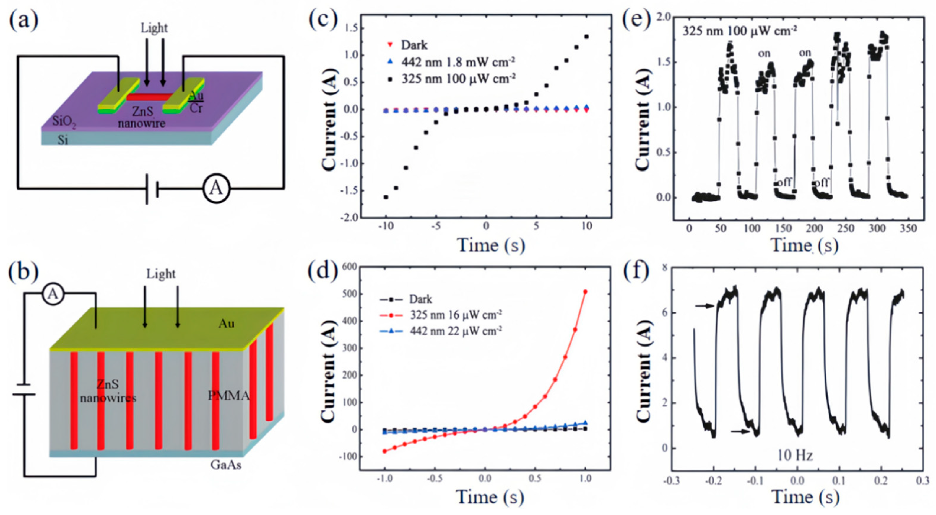
Zinc Sulfide (ZnS)-Based Photodetectors
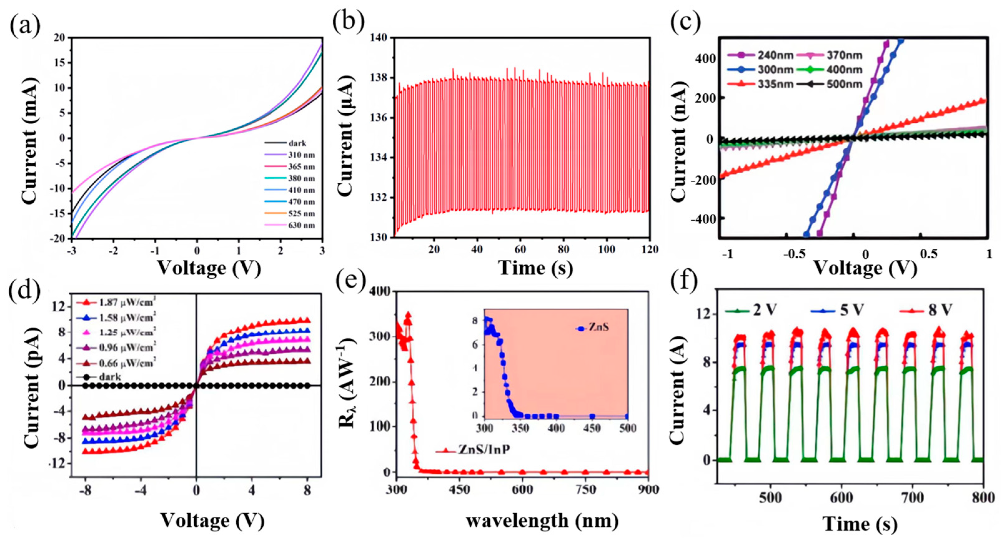
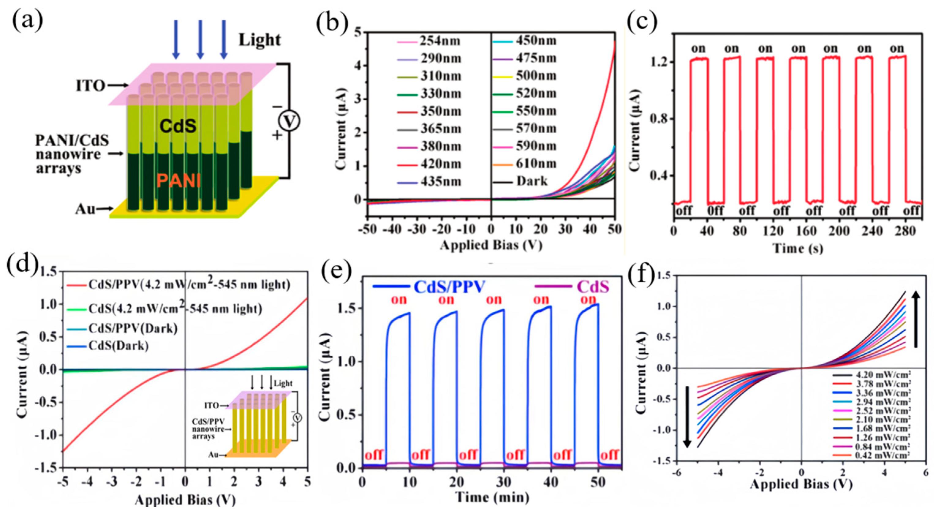
Cadmium Sulfide (CdS)-Based Photodetectors
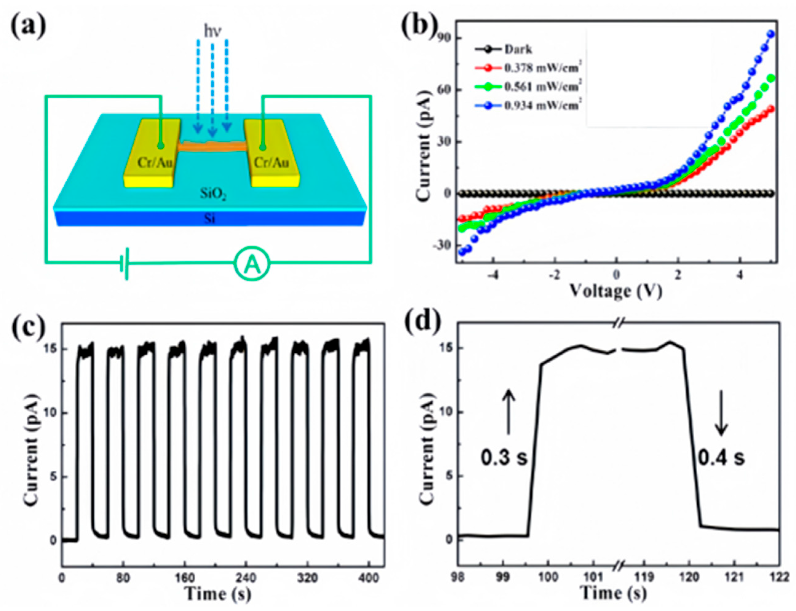
Tin Sulfide (SnS)-Based Photodetectors
Comparative Analysis
3.2.2. Photodetectors Based on Disulfide Metal Compounds
Selenium Sulfide (SnS2)-Based Photodetectors
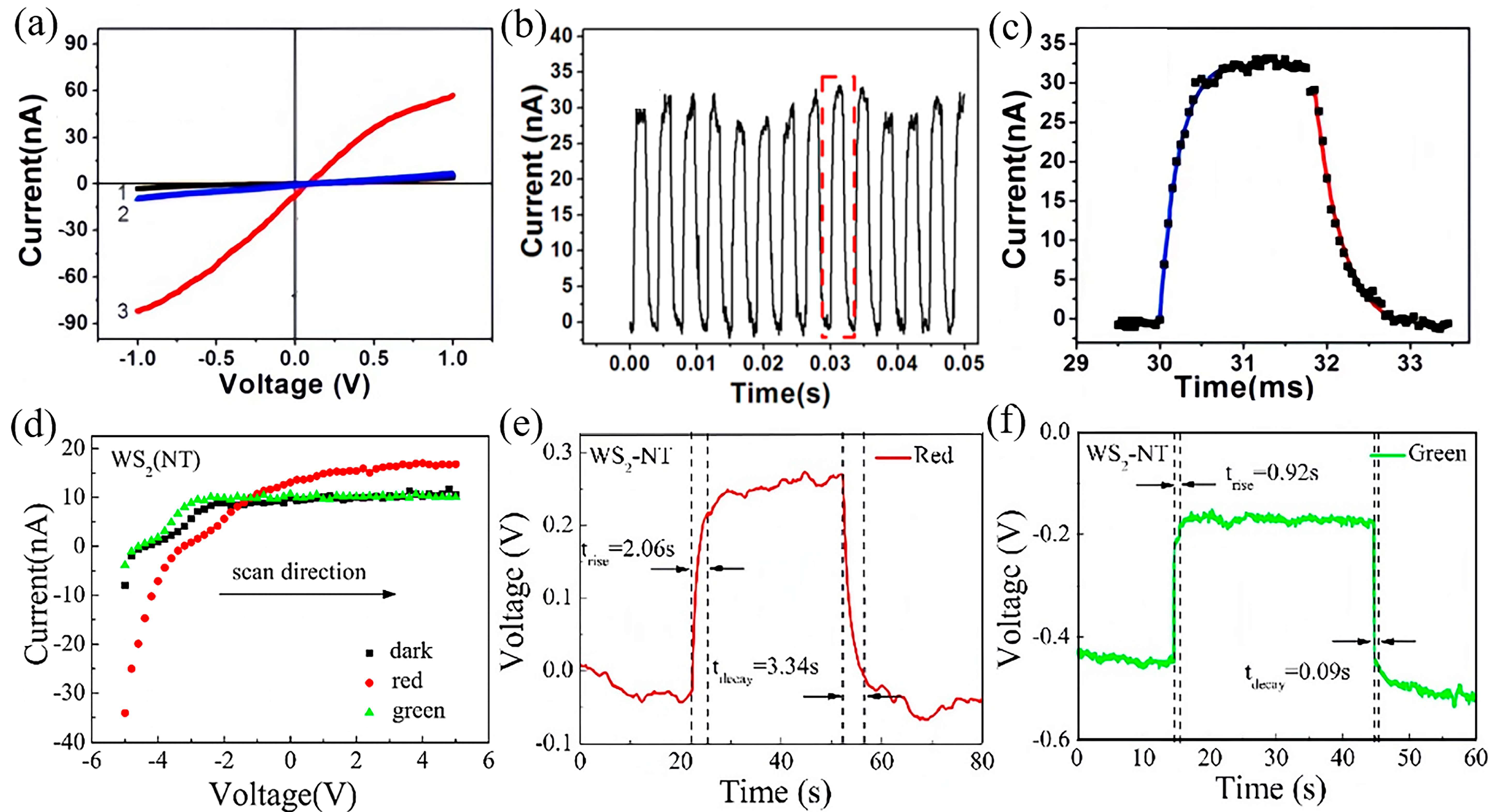
Tungsten Sulfide (WS2)-Based Photodetectors
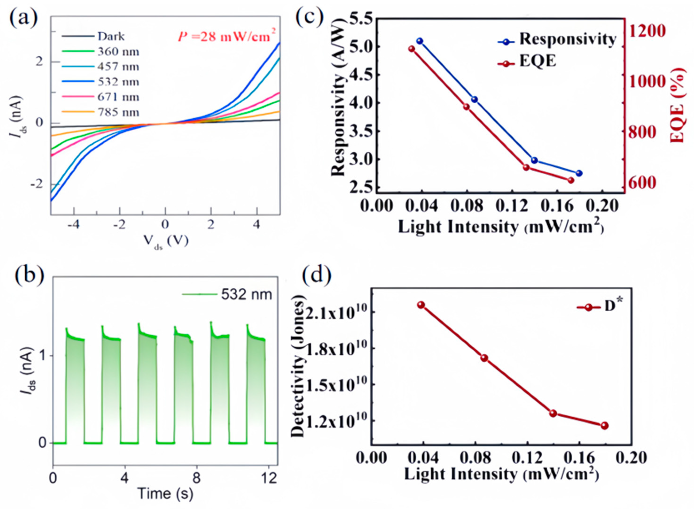
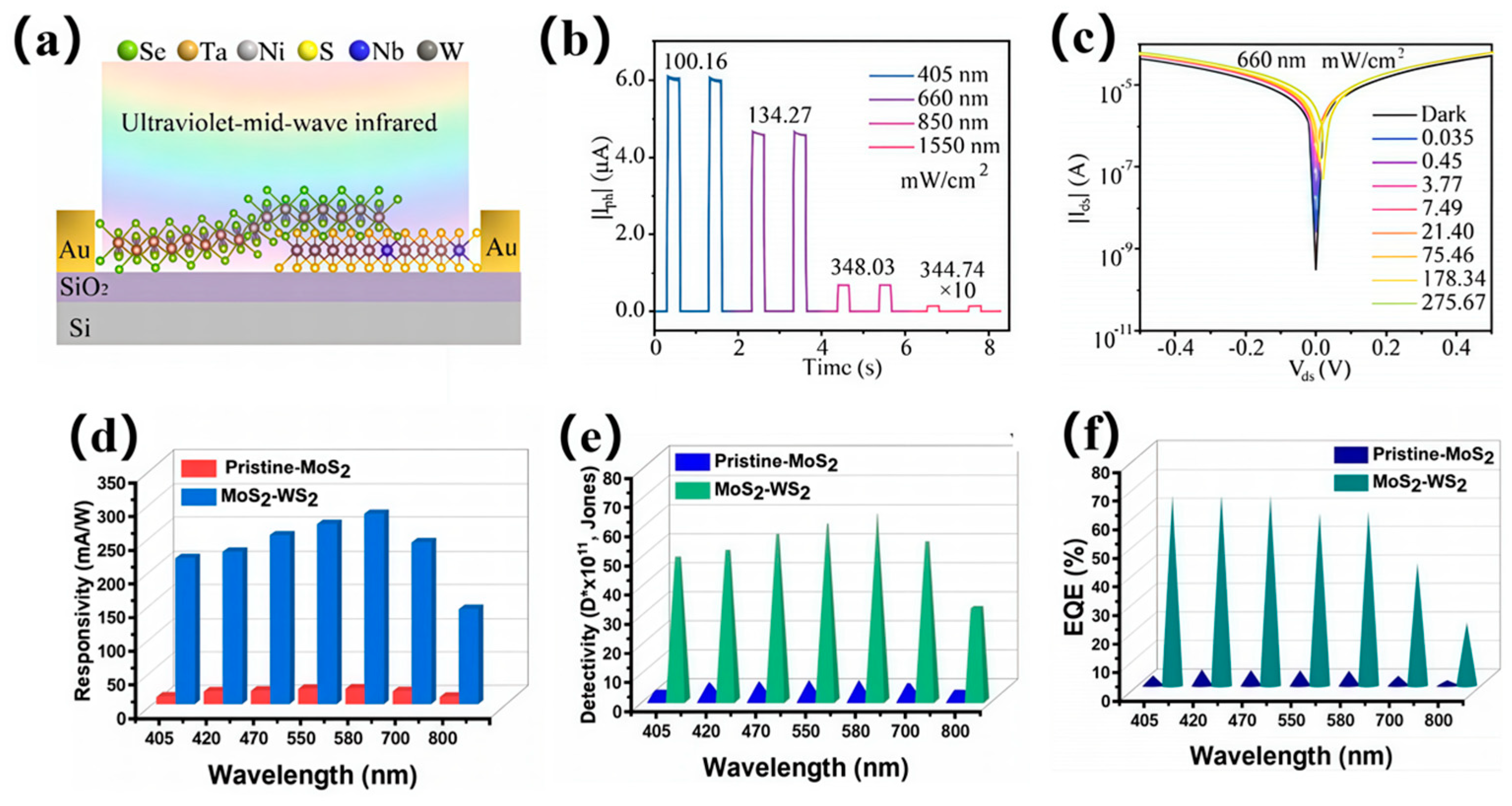
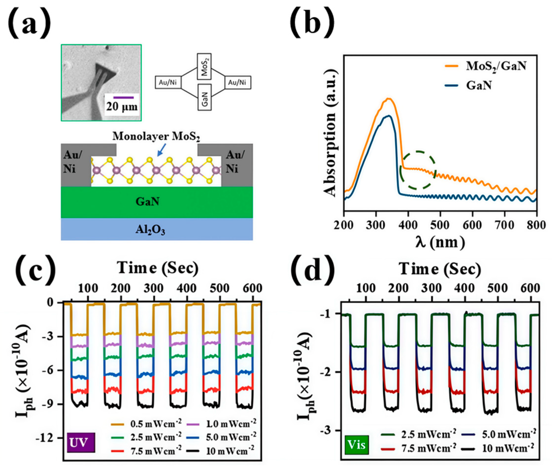
Other Metal Disulfide (MoS2, ReS2)-Based Photodetectors
Comparative Analysis
3.2.3. One-Dimensional Polysulfide Metal Compound-Based Photodetectors
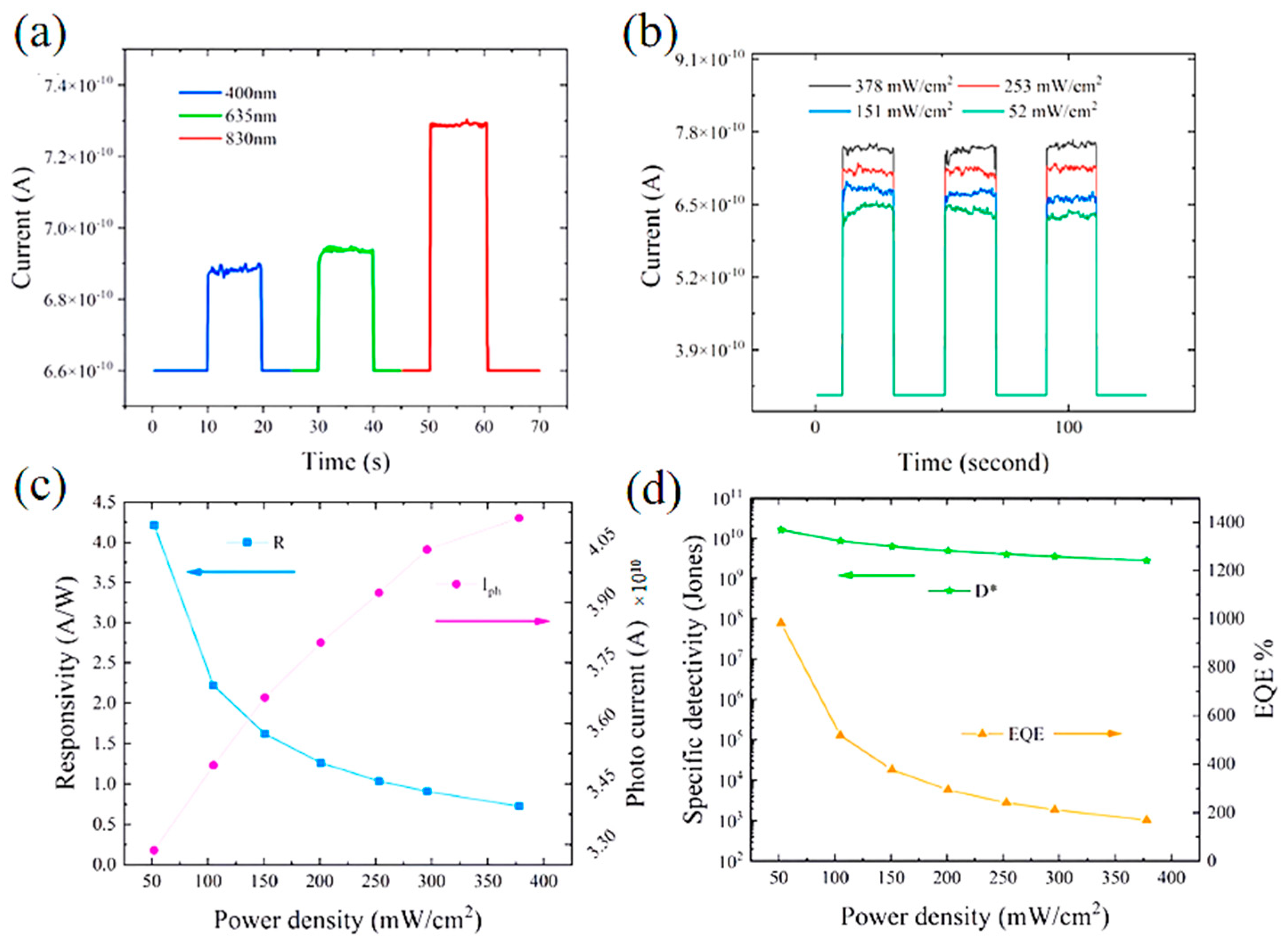
Indium Sulfide (In2S3)-Based Photodetectors
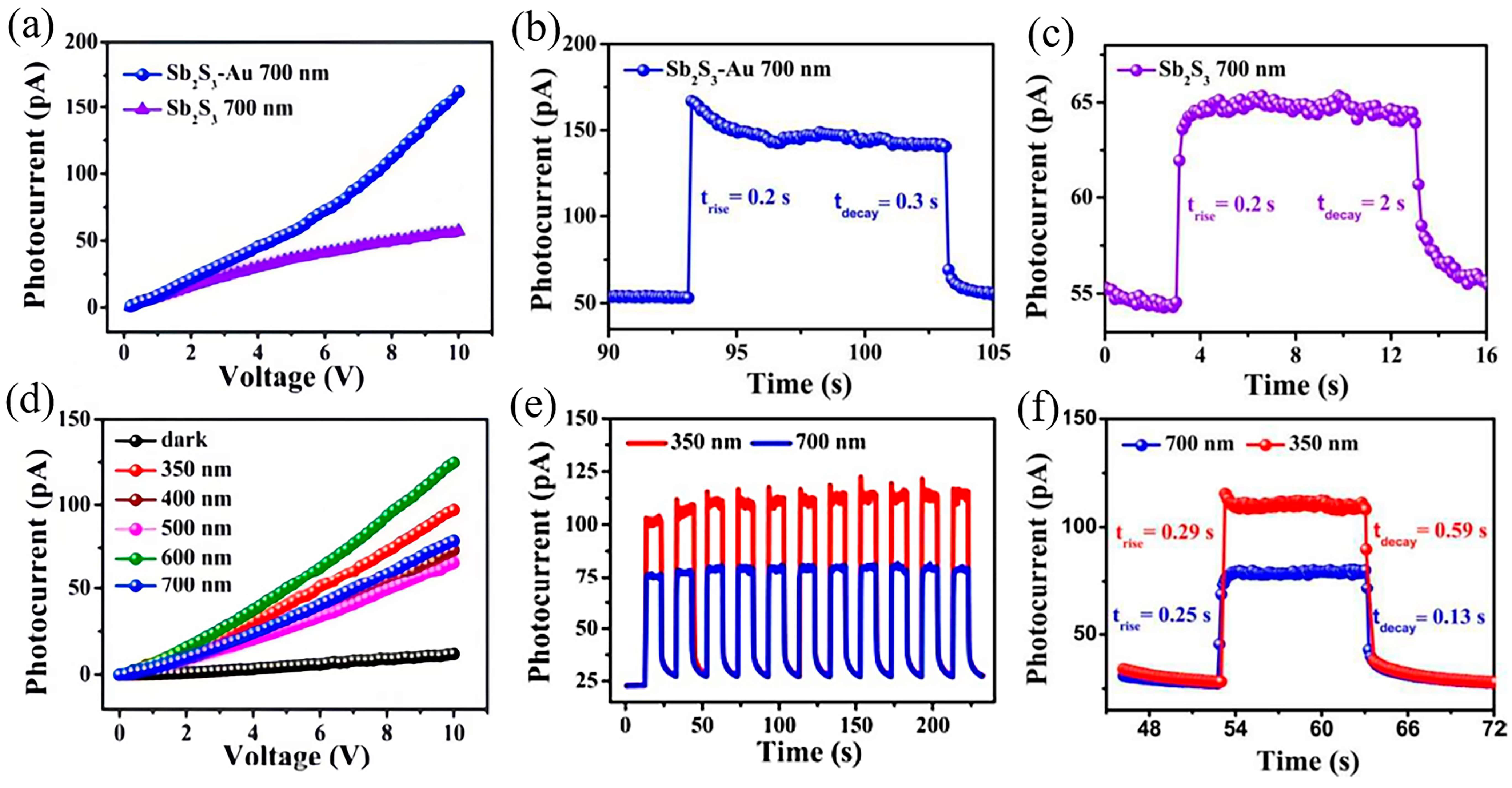
Antimony Sulfide (Sb2S3)-Based Photodetectors
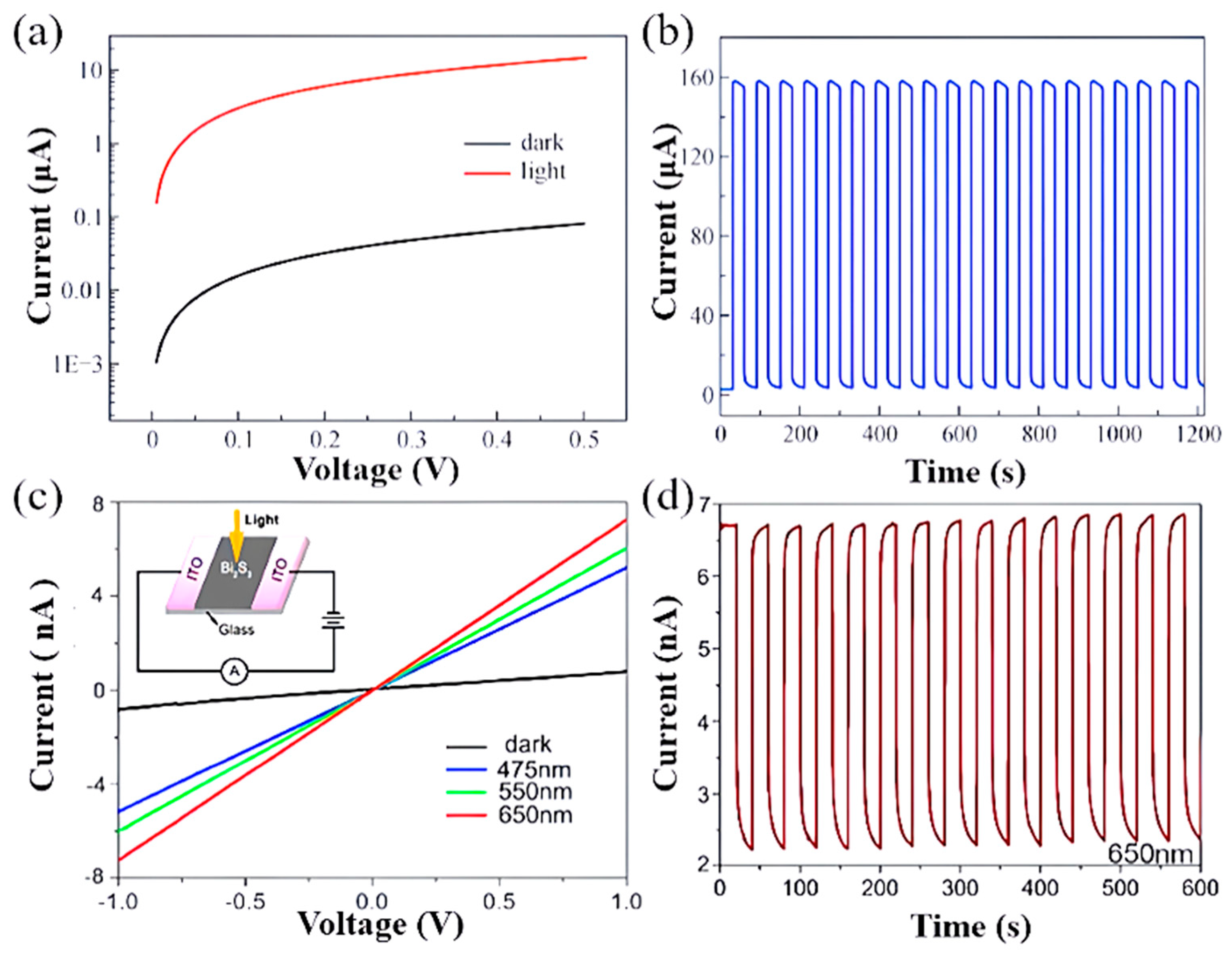
Bismuth Sulfide (Bi2S3)-Based Photodetectors
Comparative Analysis
4. Challenges and Future Prospects
4.1. Self-Powered Photodetector
4.2. Thermal Stability and Broadband Testing
4.3. Active Region
4.4. Current Limitations and Future Directions
4.4.1. Environmental Stability
4.4.2. Scalability
4.4.3. Toxicity of Cadmium-Based Materials
4.4.4. Future Research Directions
5. Conclusions and Outlook
- (1)
- When utilizing doped elements or constructing heterostructures to improve the sensitivity and responsivity of photodetectors, there remains a need to develop new, effective methods for achieving efficient detection, for example, via the polarization effect of ferroelectric polymers on the device; however, the specific effect of ferroelectric polarization on the optical response and the underlying principles need to be further studied.
- (2)
- The exploration of homogeneous hybridized nanostructures as photodetectors and the in-depth investigation of the principles at work are essential, as the complex interfaces and carrier migration pathways in hybridized nanostructures often give rise to unique optical and photoelectronic properties.
- (3)
- Due to the flexibility, transparency, and low cost of organic materials, the study of nanostructured material photodetectors with different polymer modifications can lead to the development of more stable and flexible devices while reducing costs.
- (4)
- Devices with high thermal stability and self-powering capabilities not only contribute significantly to energy conservation and emissions reduction but also offer critical utility in harsh environmental exploration. Consequently, the development of high-performance thermally stable materials and the realization of efficient devices under zero-bias conditions remain pressing challenges that demand accelerated exploration by researchers.
- (5)
- Finally, although numerous methodologies exist for material synthesis and device fabrication, synthesis processes remain challenging to control effectively. Furthermore, device manufacturing typically involves integrated processes combining photolithography, etching, and deposition. Undoubtedly, such inherently complex and time-consuming procedures hinder economic viability. Consequently, advancing fabrication techniques to streamline these processes remains a critical area for exploration.
Author Contributions
Funding
Data Availability Statement
Acknowledgments
Conflicts of Interest
References
- Kim, J.; Lee, J.; Lee, J.M.; Facchetti, A.; Marks, T.J.; Park, S.K. Recent Advances in Low-Dimensional Nanomaterials for Photodetectors. Small Methods 2023, 8, 2300246. [Google Scholar] [CrossRef]
- Paras; Yadav, K.; Kumar, P.; Teja, D.R.; Chakraborty, S.; Chakraborty, M.; Mohapatra, S.S.; Sahoo, A.; Chou, M.M.C.; Liang, C.T.; et al. A Review on Low-Dimensional Nanomaterials: Nanofabrication, Characterization and Applications. Nanomaterials 2022, 13, 160. [Google Scholar] [CrossRef] [PubMed]
- Zhao, Y.S.; Fu, H.; Peng, A.; Ma, Y.; Xiao, D.; Yao, J. Low-Dimensional Nanomaterials Based on Small Organic Molecules: Preparation and Optoelectronic Properties. Adv. Mater. 2008, 20, 2859–2876. [Google Scholar] [CrossRef]
- Chen, G.; Shrestha, L.K.; Ariga, K. Zero-to-Two Nanoarchitectonics: Fabrication of Two-Dimensional Materials from Zero-Dimensional Fullerene. Molecules 2021, 26, 4636. [Google Scholar] [CrossRef]
- Chen, Y.; Lai, Z.; Zhang, X.; Fan, Z.; He, Q.; Tan, C.; Zhang, H. Phase engineering of nanomaterials. Nat. Rev. Chem. 2020, 4, 243–256. [Google Scholar] [CrossRef] [PubMed]
- Liu, S.; Pan, X.; Liu, H. Two-Dimensional Nanomaterials for Photothermal Therapy. Angew. Chem. Int. Ed. 2020, 59, 5890–5900. [Google Scholar] [CrossRef]
- Shulga, A.G.; Derenskyi, V.; Salazar-Rios, J.M.; Dirin, D.N.; Fritsch, M.; Kovalenko, M.V.; Scherf, U.; Loi, M.A. An All-Solution-Based Hybrid CMOS-Like Quantum Dot/Carbon Nanotube Inverter. Adv. Mater. 2017, 29, 1701764. [Google Scholar] [CrossRef]
- Wang, H.P.; Li, S.; Liu, X.; Shi, Z.; Fang, X.; He, J.H. Low-Dimensional Metal Halide Perovskite Photodetectors. Adv. Mater. 2020, 33, 2003309. [Google Scholar] [CrossRef]
- Zhai, W.; Zhou, K. Nanomaterials in Superlubricity. Adv. Funct. Mater. 2019, 29, 1806395. [Google Scholar] [CrossRef]
- Zhang, H.; Fan, T.; Chen, W.; Li, Y.; Wang, B. Recent advances of two-dimensional materials in smart drug delivery nano-systems. Bioact. Mater. 2020, 5, 1071–1086. [Google Scholar] [CrossRef]
- Chi, X.; Lan, Z.A.; Chen, Q.; Zhang, X.; Chen, X.; Zhang, G.; Wang, X. Electronic Transmission Channels Promoting Charge Separation of Conjugated Polymers for Photocatalytic CO2 Reduction with Controllable Selectivity. Angew. Chem. Int. Ed. 2023, 62, e202303785. [Google Scholar] [CrossRef] [PubMed]
- Das, S.; Senapati, S.; Naik, R. 1D metal telluride heterostructure: A review on its synthesis for multifunctional applications. J. Alloys Compd. 2023, 968, 171923. [Google Scholar] [CrossRef]
- Lin, H.; Yang, L.; Zhang, X.; Liu, G.; Zhuo, S.; Chen, J.; Song, J. Emerging Low-Dimensional Nanoagents for Bio-Microimaging. Adv. Funct. Mater. 2020, 30, 2003147. [Google Scholar] [CrossRef]
- Sun, H.; Deng, J.; Qiu, L.; Fang, X.; Peng, H. Recent progress in solar cells based on one-dimensional nanomaterials. Energy Environ. Sci. 2015, 8, 1139–1159. [Google Scholar] [CrossRef]
- Xu, J.; Li, Q.; Liu, X.; Yang, Q. P-doped nanorod MoO3 and nanoflower NiAl-LDH construct S-type heterojunction for photocatalytic high-efficiency hydrogen evolution. Surf. Interfaces 2023, 43, 103593. [Google Scholar] [CrossRef]
- Peng, G.; Wu, J.; Wu, S.; Xu, X.; Ellis, J.E.; Xu, G.; Star, A.; Gao, D. Perovskite solar cells based on bottom-fused TiO2 nanocones. J. Mater. Chem. A 2016, 4, 1520–1530. [Google Scholar] [CrossRef]
- Shen, Q.; Xu, T.; Zhuang, G.-l.; Zhuang, Y.; Sun, L.; Han, X.; Wang, X.; Zhan, W. Spatially Separated Photoinduced Charge Carriers for the Enhanced Photocatalysis Over the One-Dimensional Yolk–Shell In2Se3@N-C Nanoreactor. ACS Catal. 2021, 11, 12931–12939. [Google Scholar] [CrossRef]
- Wei, D.; Dadey, A.A.; McArthur, J.A.; Bank, S.R.; Campbell, J.C. Enhancing Extended SWIR Al0.3InAsSb PIN Photodetectors with All-Dielectric Amorphous Germanium Photon-Capturing Gratings. ACS Photonics 2024, 11, 484–488. [Google Scholar] [CrossRef]
- Chen, K.; Wang, X.; Zou, C.; Liu, Q.; Chen, K.; Shi, Y.; Xu, T.; Zhao, W.; He, L.; Gao, F.; et al. Two-In-One: End-Emitting Blue LED and Self-Powered UV Photodetector based on Single Trapezoidal PIN GaN Microwire for Ambient Light UV Monitoring and Feedback. Small Methods 2023, 7, 2300138. [Google Scholar] [CrossRef]
- Chen, Y.C.; Lu, Y.J.; Liu, Q.; Lin, C.N.; Guo, J.; Zang, J.H.; Tian, Y.Z.; Shan, C.X. Ga2O3 photodetector arrays for solar-blind imaging. J. Mater. Chem. C 2019, 7, 2557–2562. [Google Scholar] [CrossRef]
- Li, G.; Wang, Y.; Huang, L.; Sun, W. Research Progress of High-Sensitivity Perovskite Photodetectors: A Review of Photodetectors: Noise, Structure, and Materials. ACS Appl. Electron. Mater. 2022, 4, 1485–1505. [Google Scholar] [CrossRef]
- Luo, M.C.; Ren, F.F.; Gagrani, N.; Qiu, K.; Wang, Q.; Yu, L.; Ye, J.; Yan, F.; Zhang, R.; Tan, H.H.; et al. Polarization-Independent Indium Phosphide Nanowire Photodetectors. Adv. Opt. Mater. 2020, 8, 2000514. [Google Scholar] [CrossRef]
- Yang, D.; Ma, D. Development of Organic Semiconductor Photodetectors: From Mechanism to Applications. Adv. Opt. Mater. 2018, 7, 1800522. [Google Scholar] [CrossRef]
- Huang, Y.C.; Parimi, V.; Chang, W.C.; Syu, H.J.; Su, Z.C.; Lin, C.F. Silicon-Based Photodetector for Infrared Telecommunication Applications. IEEE Photonics J. 2021, 13, 1–7. [Google Scholar] [CrossRef]
- Zhang, H.; Wang, W.; Yip, S.; Li, D.; Li, F.; Lan, C.; Wang, F.; Liu, C.; Ho, J.C. Enhanced performance of near-infrared photodetectors based on InGaAs nanowires enabled by a two-step growth method. J. Mater. Chem. C 2020, 8, 17025–17033. [Google Scholar] [CrossRef]
- Ding, M.; Liang, K.; Yu, S.; Zhao, X.; Ren, H.; Zhu, B.; Hou, X.; Wang, Z.; Tan, P.; Huang, H.; et al. Aqueous-Printed Ga2O3 Films for High-Performance Flexible and Heat-Resistant Deep Ultraviolet Photodetector and Array. Adv. Opt. Mater. 2022, 10, 2200512. [Google Scholar] [CrossRef]
- Ghosh, C.; Dey, A.; Biswas, I.; Gupta, R.K.; Yadav, V.S.; Yadav, A.; Yadav, N.; Zheng, H.; Henini, M.; Mondal, A. CuO–TiO2 based self-powered broad band photodetector. Nano Mater. Sci. 2024, 6, 345–354. [Google Scholar] [CrossRef]
- Guo, Y.; Zhou, J.; Zhao, F.; Wu, Y.; Tao, J.; Zuo, S.; Jiang, J.; Hu, Z.; Chu, J. Carbon-based 2D-layered Rb0.15Cs2.85Sb2ClxI9−x solar cells with superior open-voltage up to 0.88 V. Nano Energy 2021, 88, 106281. [Google Scholar] [CrossRef]
- Jain, R.K.; Khanna, A. CuO-doped WO3 thin film H2S sensors. Sens. Actuators B Chem. 2021, 343, 130153. [Google Scholar] [CrossRef]
- Li, M.; Mao, D.; Wan, J.; Wang, F.; Zhai, T.; Wang, D. Hollow multi-shell structured SnO2with enhanced performance for ultraviolet photodetectors. Inorg. Chem. Front. 2019, 6, 1968–1972. [Google Scholar] [CrossRef]
- Long, Z.; Xu, X.; Yang, W.; Hu, M.; Shtansky, D.V.; Golberg, D.; Fang, X. Cross-Bar SnO2-NiO Nanofiber-Array-Based Transparent Photodetectors with High Detectivity. Adv. Electron. Mater. 2019, 6, 1901048. [Google Scholar] [CrossRef]
- Lu, Y.C.; Zhang, Z.F.; Yang, X.; He, G.H.; Lin, C.N.; Chen, X.X.; Zang, J.H.; Zhao, W.B.; Chen, Y.C.; Zhang, L.L.; et al. High-performance solar-blind photodetector arrays constructed from Sn-doped Ga2O3 microwires via patterned electrodes. Nano Res. 2022, 15, 7631–7638. [Google Scholar] [CrossRef]
- Mondal, S.; Basak, D. Very high photoresponse towards low-powered UV light under low-biased condition by nanocrystal assembled TiO2 film. Appl. Surf. Sci. 2018, 427, 814–822. [Google Scholar] [CrossRef]
- Ouyang, W.; Chen, J.; Shi, Z.; Fang, X. Self-powered UV photodetectors based on ZnO nanomaterials. Appl. Phys. Rev. 2021, 8, 031315. [Google Scholar] [CrossRef]
- Puntsagdorj, S.; Koirala, A.R.; Gombovanjil, J.; Khanh, N.N.; Sung, S.D.; Lee, W.I.; Yoon, K.B. Increase in Photocurrent Density of WO3 Photoanode by Placing a Layer of an Ordered Array of Mesoporous WO3 Micropillars on Top of a WO3 Sheet Layer. ACS Appl. Mater. Interfaces 2022, 14, 31838–31850. [Google Scholar] [CrossRef]
- Yin, B.; Zhang, H.; Qiu, Y.; Luo, Y.; Zhao, Y.; Hu, L. Piezo-phototronic effect enhanced self-powered and broadband photodetectors based on Si/ZnO/CdO three-component heterojunctions. Nano Energy 2017, 40, 440–446. [Google Scholar] [CrossRef]
- Nam, C.Y.; Stein, A. Extreme Carrier Depletion and Superlinear Photoconductivity in Ultrathin Parallel-Aligned ZnO Nanowire Array Photodetectors Fabricated by Infiltration Synthesis. Adv. Opt. Mater. 2017, 5, 1700807. [Google Scholar] [CrossRef]
- Ouyang, W.; Teng, F.; He, J.H.; Fang, X. Enhancing the Photoelectric Performance of Photodetectors Based on Metal Oxide Semiconductors by Charge-Carrier Engineering. Adv. Funct. Mater. 2019, 29, 1807672. [Google Scholar] [CrossRef]
- Tian, W.; Lu, H.; Li, L. Nanoscale ultraviolet photodetectors based on onedimensional metal oxide nanostructures. Nano Res. 2015, 8, 382–405. [Google Scholar] [CrossRef]
- Wang, Y.; Yang, L.; Huang, M.; Kang, Y.; Wang, L.; Zhang, N. A Novel Self-Powered and High Switching Ratio UV–vis Photodetector Based on Multilayer Bi2O3/In2O3 Heterojunction. Phys. Status Solidi (RRL) Rapid Res. Lett. 2024, 18, 2300456. [Google Scholar] [CrossRef]
- Wang, Z.; Wang, P.; Wang, F.; Ye, J.; He, T.; Wu, F.; Peng, M.; Wu, P.; Chen, Y.; Zhong, F.; et al. A Noble Metal Dichalcogenide for High-Performance Field-Effect Transistors and Broadband Photodetectors. Adv. Funct. Mater. 2019, 30, 1907945. [Google Scholar] [CrossRef]
- Xu, Y.; Shen, H.; Zhang, J.; Zhao, Q.; Wang, Z.; Xu, B.; Zhang, W. High-performance CuS/n-Si heterojunction photodetectors prepared by e-beam evaporation of Cu films as precursor layers. J. Alloys Compd. 2021, 884, 161121. [Google Scholar] [CrossRef]
- Singh, S.V.; Sharma, A.; Biring, S.; Pal, B.N. Solution processed Cu2S/TiO2 heterojunction for visible-near infrared photodetector. Thin Solid Film. 2020, 710, 138275. [Google Scholar] [CrossRef]
- Wu, J.J.; Tao, Y.R.; Wu, Y.; Wu, X.C. Ultrathin SnS2 nanosheets of ultrasonic synthesis and their photoresponses from ultraviolet to near-infrared. Sens. Actuators B Chem. 2016, 231, 211–217. [Google Scholar] [CrossRef]
- Jiang, J.; Xu, W.; Guo, F.; Yang, S.; Ge, W.; Shen, B.; Tang, N. Polarization-Resolved Near-Infrared PdSe2 p-i-n Homojunction Photodetector. Nano Lett. 2023, 23, 9522–9528. [Google Scholar] [CrossRef] [PubMed]
- Li, T.; Miao, J.; Fu, X.; Song, B.; Cai, B.; Ge, X.; Zhou, X.; Zhou, P.; Wang, X.; Jariwala, D.; et al. Reconfigurable, non-volatile neuromorphic photovoltaics. Nat. Nanotechnol. 2023, 18, 1303–1310. [Google Scholar] [CrossRef]
- Toe, C.Y.; Zhou, S.; Gunawan, M.; Lu, X.; Ng, Y.H.; Amal, R. Recent advances and the design criteria of metal sulfide photocathodes and photoanodes for photoelectrocatalysis. J. Mater. Chem. A 2021, 9, 20277–20319. [Google Scholar] [CrossRef]
- Hong, J.; Kim, B.S.; Yang, S.; Jang, A.R.; Lee, Y.W.; Pak, S.; Lee, S.; Cho, Y.; Kang, D.; Shin, H.S.; et al. Chalcogenide solution-mediated activation protocol for scalable and ultrafast synthesis of single-crystalline 1-D copper sulfide for supercapacitors. J. Mater. Chem. A 2019, 7, 2529–2535. [Google Scholar] [CrossRef]
- Sun, L.; Leong, W.S.; Yang, S.; Chisholm, M.F.; Liang, S.J.; Ang, L.K.; Tang, Y.; Mao, Y.; Kong, J.; Yang, H.Y. Concurrent Synthesis of High-Performance Monolayer Transition Metal Disulfides. Adv. Funct. Mater. 2017, 27, 1605896. [Google Scholar] [CrossRef]
- Wang, L.; Fan, Y.; Han, G.; Ben, H.; Lin, C.; Ma, C. Engineering fast diffusion channels in metal Sulfide/Selenide heterostructures via confinement effect for high-performance sodium storage. Chem. Eng. J. 2024, 493, 152732. [Google Scholar] [CrossRef]
- Wang, P.; Zhang, X.; Zhang, J.; Wan, S.; Guo, S.; Lu, G.; Yao, J.; Huang, X. Precise tuning in platinum-nickel/nickel sulfide interface nanowires for synergistic hydrogen evolution catalysis. Nat. Commun. 2017, 8, 14580. [Google Scholar] [CrossRef] [PubMed]
- Li, Y.; Tang, L.; Li, R.; Xiang, J.; Teng, K.S.; Lau, S.P. SnS2 quantum dots: Facile synthesis, properties, and applications in ultraviolet photodetector. Chin. Phys. B 2019, 28, 037801. [Google Scholar] [CrossRef]
- Gao, W.; Zhang, S.; Zhang, F.; Wen, P.; Zhang, L.; Sun, Y.; Chen, H.; Zheng, Z.; Yang, M.; Luo, D. 2D WS2 based asymmetric Schottky photodetector with high performance. Adv. Electron. Mater. 2021, 7, 2000964. [Google Scholar] [CrossRef]
- Zhang, C.; Wang, S.; Yang, L.; Liu, Y.; Xu, T.; Ning, Z.; Zak, A.; Zhang, Z.; Tenne, R.; Chen, Q. High-performance photodetectors for visible and near-infrared lights based on individual WS2 nanotubes. Appl. Phys. Lett. 2012, 100, 243101. [Google Scholar] [CrossRef]
- Freitag, M.; Low, T.; Xia, F.; Avouris, P. Photoconductivity of biased graphene. Nat. Photonics 2012, 7, 53–59. [Google Scholar] [CrossRef]
- Han, S. New developments in photoconductive detectors (invited). Rev. Sci. Instrum. 1997, 68, 647–652. [Google Scholar] [CrossRef]
- Silva, J.P.B.; Vieira, E.M.F.; Gwozdz, K.; Silva, N.E.; Kaim, A.; Istrate, M.C.; Ghica, C.; Correia, J.H.; Pereira, M.; Marques, L.; et al. High-performance and self-powered visible light photodetector using multiple coupled synergetic effects. Mater. Horiz. 2024, 11, 803–812. [Google Scholar] [CrossRef] [PubMed]
- Won, U.Y.; Lee, B.H.; Kim, Y.R.; Kang, W.T.; Lee, I.; Kim, J.E.; Lee, Y.H.; Yu, W.J. Efficient photovoltaic effect in graphene/h-BN/silicon heterostructure self-powered photodetector. Nano Res. 2020, 14, 1967–1972. [Google Scholar] [CrossRef]
- Liu, S.; Tian, J.; Wu, S.; Zhang, W.; Luo, M. A bioinspired broadband self-powered photodetector based on photo-pyroelectric-thermoelectric effect able to detect human radiation. Nano Energy 2022, 93, 106812. [Google Scholar] [CrossRef]
- Liu, Y.; Hu, Q.; Cao, Y.; Wang, P.; Wei, J.; Wu, W.; Wang, J.; Huang, F.; Sun, J.L. High-Performance Ultrabroadband Photodetector Based on Photothermoelectric Effect. ACS Appl. Mater. Interfaces 2022, 14, 29077–29086. [Google Scholar] [CrossRef]
- Ma, N.; Yang, Y. Enhanced self-powered UV photoresponse of ferroelectric BaTiO3 materials by pyroelectric effect. Nano Energy 2017, 40, 352–359. [Google Scholar] [CrossRef]
- Wu, M.; Jiang, Z.; Lou, X.; Zhang, F.; Song, D.; Ning, S.; Guo, M.; Pennycook, S.J.; Dai, J.Y.; Wen, Z. Flexoelectric Thin-Film Photodetectors. Nano Lett. 2021, 21, 2946–2952. [Google Scholar] [CrossRef] [PubMed]
- Jiang, A.; Xing, S.; Lin, H.; Chen, Q.; Li, M. Role of Pyramidal Low-Dimensional Semiconductors in Advancing the Field of Optoelectronics. Photonics 2024, 11, 370. [Google Scholar] [CrossRef]
- Morkoc, H.; Omnès, F.; Litton, C.W.; Monroy, E.; Muñoz, E.; Reverchon, J.L. Wide bandgap UV photodetectors: A short review of devices and applications. Gallium Nitride Mater. Devices II 2007, 6473, 111–125. [Google Scholar]
- Yadav, P.V.K.; Ajitha, B.; Kumar Reddy, Y.A.; Sreedhar, A. Recent advances in development of nanostructured photodetectors from ultraviolet to infrared region: A review. Chemosphere 2021, 279, 130473. [Google Scholar] [CrossRef]
- Vosk, R.; Huse, D.A.; Altman, E. Theory of the Many-Body Localization Transition in One-Dimensional Systems. Phys. Rev. X 2015, 5, 031032. [Google Scholar] [CrossRef]
- Yang, Y.; Lin, J.; Huang, Y.; Zhang, Y.; Wang, M.; Zhu, X.; Guo, J.; Fan, K.; Ao, J.; Li, J.; et al. Vertical van der Waals Integrated p-W0.09Re0.91S2 /GaN Heterojunction for Ultra-High Detectivity UV Image Sensing. Laser Photonics Rev. 2024, 19, 2401142. [Google Scholar] [CrossRef]
- Ahmad, M.; Pan, C.; Zhao, J.; Zhu, J. Impact of Pb Doping on the Optical and Electrical Properties of ZnO Nanowires. J. Nanosci. Nanotechnol. 2011, 11, 1950–1957. [Google Scholar] [CrossRef]
- Kim, C.; Han, S.; Kim, T.; Lee, S. Implantable pH Sensing System Using Vertically Stacked Silicon Nanowire Arrays and Body Channel Communication for Gastroesophageal Reflux Monitoring. Sensors 2024, 24, 861. [Google Scholar] [CrossRef]
- Xu, J.; Li, H.; Fang, S.; Jiang, K.; Yao, H.; Fang, F.; Chen, F.; Wang, Y.; Shi, Y. Synthesis of bismuth sulfide nanobelts for high performance broadband photodetectors. J. Mater. Chem. C 2020, 8, 2102–2108. [Google Scholar] [CrossRef]
- Gao, H.; Cao, J.; Li, T.; Luo, W.; Gray, M.; Kumar, N.; Burch, K.S.; Ling, X. Phase-Controllable Synthesis of Ultrathin Molybdenum Nitride Crystals Via Atomic Substitution of MoS2. Chem. Mater. 2021, 34, 351–357. [Google Scholar] [CrossRef]
- Lei, H.; Yang, G.; Zheng, X.; Zhang, Z.G.; Chen, C.; Ma, J.; Guo, Y.; Chen, Z.; Qin, P.; Li, Y.; et al. Incorporation of High-Mobility and Room-Temperature-Deposited CuxS as a Hole Transport Layer for Efficient and Stable Organo-Lead Halide Perovskite Solar Cells. Sol. RRL 2017, 1, 1700038. [Google Scholar] [CrossRef]
- Gao, J.; Chen, R.; Li, D.H.; Jiang, L.; Ye, J.C.; Ma, X.C.; Chen, X.D.; Xiong, Q.H.; Sun, H.D.; Wu, T. UV light emitting transparent conducting tin-doped indium oxide (ITO) nanowires. Nanotechnology 2011, 22, 195706. [Google Scholar] [CrossRef] [PubMed]
- Chen, Z.; Lin, X.; Lin, S.; Ren, J.; Wan, L.; Peng, B. Inverted-Structural Self-Powered Gan/PZT/ITO UV Photodetector Enhanced by Ferroelectric Modulation. Adv. Electron. Mater. 2023, 10, 2300588. [Google Scholar] [CrossRef]
- Wu, P.; Song, X.; Si, S.; Ke, Z.; Cheng, L.; Li, W.; Xiao, X.; Jiang, C. Significantly enhanced visible light response in single TiO2 nanowire by nitrogen ion implantation. Nanotechnology 2018, 29, 184005. [Google Scholar] [CrossRef]
- Sirkeli, V.P.; Yilmazoglu, O.; Hajo, A.S.; Nedeoglo, N.D.; Nedeoglo, D.D.; Preu, S.; Küppers, F.; Hartnagel, H.L. Enhanced responsivity of ZnSe-based metal–semiconductor–metal near-ultraviolet photodetector via impact ionization. Phys. Status Solidi (RRL)–Rapid Res. Lett. 2018, 12, 1700418. [Google Scholar] [CrossRef]
- Singh, A.K.; Chowdhury, N.K.; Hazra, A.; Bhowmik, B. Room-Temperature Au/TiO2 Nanorods/Ti TFT Butanone Sensor: Role of Surface States. J. Electron. Mater. 2023, 52, 3622–3632. [Google Scholar] [CrossRef]
- Sirkeli, V.P.; Yilmazoglu, O.; Hajo, A.S.; Nedeoglo, N.D.; Nedeoglo, D.D.; Küppers, F.; Hartnagel, H.L. High Performance ZnSe-Based Metal–Semiconductor–Metal Ultraviolet Photodetectors with Different Schottky Contacts. Phys. Solid State 2024, 66, 257–264. [Google Scholar] [CrossRef]
- Dahiya, S.; Hazra, S.; Pandey, U.; Pramanik, S.; Dahiya, P.; Singh, S.V.; Kumari, N.; Pal, B.N. Enhancement in photo-response of CuZnS nanocrystals-based photodetector using asymmetric work function electrodes. Opt. Mater. 2024, 157, 116182. [Google Scholar] [CrossRef]
- Yang, Z.; Liu, M.; Li, W.; Xu, J.; Wan, P.; Xu, T.; Shi, D.; Kan, C.; Jiang, M. Boosting photoresponses in a SnO2 microwire heterojunction ultraviolet self-biased photodetector through tailoring heterointerface. Surf. Interfaces 2024, 46, 104001. [Google Scholar] [CrossRef]
- Zhang, L.; Geng, X.; Zha, G.; Xu, J.; Wei, S.; Ma, B.; Chen, Z.; Shang, X.; Ni, H.; Niu, Z. Self-catalyzed molecular beam epitaxy growth and their optoelectronic properties of vertical GaAs nanowires on Si(111). Mater. Sci. Semicond. Process. 2016, 52, 68–74. [Google Scholar] [CrossRef]
- Hsieh, Y.-Y.; Tuan, H.-Y. Architectural van der Waals Bi2S3/Bi2Se3 topological heterostructure as a superior potassium-ion storage material. Energy Storage Mater. 2022, 51, 789–805. [Google Scholar] [CrossRef]
- Li, D.; Liu, Y.; Shi, W.; Shao, C.; Wang, S.; Ding, C.; Liu, T.; Fan, F.; Shi, J.; Li, C. Crystallographic-orientation-dependent charge separation of BiVO4 for solar water oxidation. ACS Energy Lett. 2019, 4, 825–831. [Google Scholar] [CrossRef]
- He, B.; Jia, S.; Zhao, M.; Wang, Y.; Chen, T.; Zhao, S.; Li, Z.; Lin, Z.; Zhao, Y.; Liu, X. General and Robust Photothermal-Heating-Enabled High-Efficiency Photoelectrochemical Water Splitting. Adv. Mater. 2021, 33, 2004406. [Google Scholar] [CrossRef] [PubMed]
- Hu, Z.; Ying, L.; Huang, F.; Cao, Y. Towards a bright future: Polymer solar cells with power conversion efficiencies over 10%. Sci. China Chem. 2017, 60, 571–582. [Google Scholar] [CrossRef]
- Ren, Z.; Wang, Q.; Zhang, G.; Zhang, T.; Liu, J.; Wang, S.; Qiao, S. Self-powered CdS nanorods/planar-Si photodetector and its performance optimization by fully developing pyro-phototronic effect. Surf. Interfaces 2023, 42, 103495. [Google Scholar] [CrossRef]
- Li, J.; Li, R.; Wang, W.; Lan, K.; Zhao, D. Ordered Mesoporous Crystalline Frameworks Toward Promising Energy Applications. Adv. Mater. 2024, 36, 2311460. [Google Scholar] [CrossRef]
- Jamal, F.; Rafique, A.; Moeen, S.; Haider, J.; Nabgan, W.; Haider, A.; Imran, M.; Nazir, G.; Alhassan, M.; Ikram, M.; et al. Review of Metal Sulfide Nanostructures and their Applications. ACS Appl. Nano Mater. 2023, 6, 7077–7106. [Google Scholar] [CrossRef]
- Wang, C.L.; Wu, Q.Q.; Ding, Y.; Zhang, X.M.; Wang, W.H.; Guo, X.T.; Ni, Z.H.; Lin, L.G.; Cai, Z.Y.; Gu, X.F.; et al. High-Responsivity and Broadband MoS2 Photodetector Using Interfacial Engineering. ACS Appl. Mater. Interfaces 2023, 15, 46236–46246. [Google Scholar] [CrossRef]
- Zhang, G.; Guan, Z.; Yang, J.; Li, Q.; Zhou, Y.; Zou, Z. Metal Sulfides for Photocatalytic Hydrogen Production: Current Development and Future Challenges. Sol. RRL 2022, 6, 2200587. [Google Scholar] [CrossRef]
- Yoneda, K.; Toda, T.; Hishida, Y.; Niina, T. The preparation of conductive ZnS films by using MBE with a single effusion source. J. Cryst. Growth 1984, 67, 125–134. [Google Scholar] [CrossRef]
- Arsad, A.Z.; Bahrudin, M.S.; Arzaee, N.A.; Rahman, M.N.A.; Chau, C.F.; Abdullah, S.F.; Zuhdi, A.W.M. Zinc sulfide thin films deposited by chemical bath: Tuning consideration of structural, optical band gap, and electrical properties for CIGS solar cells application. Ceram. Int. 2024, 50, 11776–11786. [Google Scholar] [CrossRef]
- Azmand, A.; Kafashan, H. Physical and electrochemical properties of electrodeposited undoped and Se-doped ZnS thin films. Ceram. Int. 2018, 44, 17124–17137. [Google Scholar] [CrossRef]
- Zhao, W.; Wei, Z.; Zhang, L.; Wu, X.; Wang, X.; Jiang, J. Optical and magnetic properties of Co and Ni co-doped ZnS nanorods prepared by hydrothermal method. J. Alloys Compd. 2017, 698, 754–760. [Google Scholar] [CrossRef]
- Alzaid, M.; Alwshih, M.; Abd-el Salam, M.N.; Hadia, N.M.A. Role of Cu dilute on microstructures, optical, photoluminescence, magnetic and electrical properties of CdS film. Mater. Sci. Semicond. Process. 2021, 127, 105687. [Google Scholar] [CrossRef]
- Deng, K.; Li, L. CdS Nanoscale Photodetectors. Adv. Mater. 2014, 26, 2619–2635. [Google Scholar] [CrossRef]
- Salas-Villasenor, A.L.; Mejia, I.; Sotelo-Lerma, M.; Guo, Z.B.; Alshareef, H.N.; Quevedo-Lopez, M.A. Improved electrical stability of CdS thin film transistors through hydrogen-based thermal treatments. Semicond. Sci. Technol. 2014, 29, 085001. [Google Scholar] [CrossRef]
- Cui, Y.; Zhou, Z.; Wang, X.; Wang, X.; Ren, Z.; Pan, L.; Yang, J. Wavelength-selectivity polarization dependence of optical absorption and photoresponse in SnS nanosheets. Nano Res. 2021, 14, 2224–2230. [Google Scholar] [CrossRef]
- Gotoh, T. Control of carrier concentration in SnS films by annealing with S and Sn. Phys. Status Solidi (A) 2016, 213, 1869–1872. [Google Scholar] [CrossRef]
- Lim, D.; Suh, H.; Suryawanshi, M.; Song, G.Y.; Cho, J.Y.; Kim, J.H.; Jang, J.H.; Jeon, C.W.; Cho, A.; Ahn, S.; et al. Kinetically Controlled Growth of Phase-Pure SnS Absorbers for Thin Film Solar Cells: Achieving Efficiency Near 3% with Long-Term Stability Using an SnS/CdS Heterojunction. Adv. Energy Mater. 2018, 8, 1702605. [Google Scholar] [CrossRef]
- Jeff, J.P.M.S.; Cindy, H.X.L.; Rebecca, A.D.; Li, R.X.; Jin, L.; Ma, T.; Wilhelmus, M.M.K.; Steven, J.; Ageeth, A.B. Correction to Nb Doping and Alloying of 2D WS2 by Atomic Layer Deposition for 2D Transition Metal Dichalcogenide Transistors and HER Electrocatalysts. ACS Appl. Nano Mater 2024, 7, 12205–12206. [Google Scholar]
- Mohamed, A.B.; Shrouk, E.Z.; Yasin, R.E. Fast optoelectronic gas sensing with p-type V2O5/WS2/Si heterojunction thin film. Mater. Chem. Phys. 2023, 310, 128491. [Google Scholar]
- Aji, A.S.; Solís-Fernández, P.; Ji, H.G.; Fukuda, K.; Ago, H. High Mobility WS2 Transistors Realized by Multilayer Graphene Electrodes and Application to High Responsivity Flexible Photodetectors. Adv. Funct. Mater. 2017, 27, 1703448. [Google Scholar] [CrossRef]
- Hieu, N.N.; Ilyasov, V.V.; Vu, T.V.; Poklonski, N.A.; Phuc, H.V.; Phuong, L.T.T.; Hoi, B.D.; Nguyen, C.V. First principles study of optical properties of molybdenum disulfide: From bulk to monolayer. Superlattices Microstruct. 2018, 115, 10–18. [Google Scholar] [CrossRef]
- Lin, J.; Monaghan, S.; Sakhuja, N.; Gity, F.; Jha, R.K.; Coleman, E.M.; Connolly, J.; Cullen, C.P.; Walsh, L.A.; Mannarino, T.; et al. Large-area growth of MoS2 at temperatures compatible with integrating back-end-of-line functionality. 2D Mater. 2020, 8, 025008. [Google Scholar] [CrossRef]
- Wang, J.W.; Liu, Y.P.; Chen, P.H.; Chuang, M.H.; Pezeshki, A.; Ling, D.C.; Chen, J.C.; Chen, Y.F.; Lee, Y.H. Controlled Low-Frequency Electrical Noise of Monolayer MoS2 with Ohmic Contact and Tunable Carrier Concentration. Adv. Electron. Mater. 2017, 4, 1700340. [Google Scholar] [CrossRef]
- Yang, L.; Yuan, X.; Liu, R.; Wu, P.; Zhong, Y.; Zhu, F.; Chang, W. Intrinsic properties of metallic edge states in MoS2 nanobelt. J. Mater. Sci. Mater. Electron. 2022, 33, 23722–23728. [Google Scholar] [CrossRef]
- Huang, Y.; Sutter, E.; Sadowski, J.T.; Cotlet, M.; Monti, O.L.A.; Racke, D.A.; Neupane, M.R.; Wickramaratne, D.; Lake, R.K.; Parkinson, B.A. Tin Disulfide-An Emerging Layered Metal Dichalcogenide Semiconductor: Materials Properties and Device Characteristics. ACS Nano 2014, 8, 10743–10755. [Google Scholar] [CrossRef]
- Arulanantham, A.M.S.; Raj, P.M.; Gunavathy, K.V.; Begam, M.R.; Ganesh, V.; Algarni, H. Photosensitivity properties of Eu-doped SnS2 thin films deposited by cost-effective nebulizer spray pyrolysis technique. Appl. Phys. A 2022, 128, 364. [Google Scholar] [CrossRef]
- Pradhan, N.R.; McCreary, A.; Rhodes, D.; Lu, Z.; Feng, S.; Manousakis, E.; Smirnov, D.; Namburu, R.; Dubey, M.; Walker, A.R. Metal to Insulator Quantum-Phase Transition in Few-Layered ReS2. Nano Lett 2015, 15, 8377–8384. [Google Scholar] [CrossRef]
- Leicht, G.; Berger, H.; Levy, F. The growth of n- and p-type ReS2 and ReSe2 single crystals and their electrical properties. Solid State Commun. 1987, 61, 531–534. [Google Scholar] [CrossRef]
- Bangolla, H.K.; Yusuf Fakhri, M.; Lin, C.H.; Cheng, C.M.; Lu, Y.H.; Fu, T.Y.; Selvarasu, P.; Ulaganathan, R.K.; Sankar, R.; Chen, R.S. Electrical and optoelectronic anisotropy and surface electron accumulation in ReS2 nanostructures. Nanoscale 2023, 15, 19735–19745. [Google Scholar] [CrossRef] [PubMed]
- Liu, M.; Gong, Y.; Li, Z.; Dou, M.; Wang, F. A green and facile hydrothermal approach for the synthesis of high-quality semi-conducting Sb2S3 thin films. Appl. Surf. Sci. 2016, 387, 790–795. [Google Scholar] [CrossRef]
- Zhang, H.; Yuan, S.; Deng, H.; Ishaq, M.; Yang, X.; Hou, T.; Shah, U.A.; Song, H.; Tang, J. Controllable orientations for Sb2S3 solar cells by vertical VTD method. Prog. Photovolt. Res. Appl. 2020, 28, 823–832. [Google Scholar] [CrossRef]
- Zhong, P.; Xie, J.; Bagheri, R.; Yi, Q.; Chen, Q.; Tan, J.; He, L.; Zhang, F.; Zhang, L.; Zou, G. An aqueous solution method towards Sb2S3 thin films for photoanodes. Chem. Commun. 2019, 55, 14530–14533. [Google Scholar] [CrossRef]
- Gao, C.; Shen, H.; Sun, L.; Shen, Z. Chemical bath deposition of Bi2S3 films by a novel deposition system. Appl. Surf. Sci. 2011, 257, 7529–7533. [Google Scholar] [CrossRef]
- Ji, W.; Shi, X.L.; Liu, W.D.; Yuan, H.; Zheng, K.; Wan, B.; Shen, W.; Zhang, Z.; Fang, C.; Wang, Q.; et al. Boosting the thermoelectric performance of n-type Bi2S3 by hierarchical structure manipulation and carrier density optimization. Nano Energy 2021, 87, 106171. [Google Scholar] [CrossRef]
- Medles, M.; Benramdane, N.; Bouzidi, A.; Nakrela, A.; Tabet-Derraz, H.; Kebbab, Z.; Mathieu, C.; Khelifa, B.; Desfeux, R. Optical and electrical properties of Bi2S3 films deposited by spray pyrolysis. Thin Solid Film. 2006, 497, 58–64. [Google Scholar] [CrossRef]
- Liu, M.; Li, Z.; Ji, J.; Dou, M.; Wang, F. Properties of nanostructured pure β-In2S3 thin films prepared by sulfurization-assisted electrodeposition. J. Mater. Sci. Mater. Electron. 2016, 28, 5044–5052. [Google Scholar] [CrossRef]
- Soni, V.; Raizada, P.; Kumar, A.; Hasija, V.; Singal, S.; Singh, P.; Hosseini-Bandegharaei, A.; Thakur, V.K.; Nguyen, V.H. Indium sulfide-based photocatalysts for hydrogen production and water cleaning: A review. Environ. Chem. Lett. 2021, 19, 1065–1095. [Google Scholar] [CrossRef]
- Ferrer, I.J.; Ares, J.R.; Clamagirand, J.M.; Barawi, M.; Sánchez, C. Optical properties of titanium trisulphide (TiS3) thin films. Thin Solid Film. 2013, 535, 398–401. [Google Scholar] [CrossRef]
- Muratov, D.S.; Vanyushin, V.O.; Vorobeva, N.S.; Jukova, P.; Lipatov, A.; Kolesnikov, E.A.; Karpenkov, D.; Kuznetsov, D.V.; Sinitskii, A. Synthesis and exfoliation of quasi-1D (Zr,Ti)S3 solid solutions for device measurements. J. Alloys Compd. 2020, 815, 152316. [Google Scholar] [CrossRef]
- Tripathi, N.; Pavelyev, V.; Sharma, P.; Kumar, S.; Rymzhina, A.; Mishra, P. Review of titanium trisulfide (TiS3): A novel material for next generation electronic and optical devices. Mater. Sci. Semicond. Process. 2021, 127, 105699. [Google Scholar] [CrossRef]
- Ebrahimi, S.; Yarmand, B.; Naderi, N. ZnS-Based UV Detectors. In Handbook of II-VI Semiconductor-Based Sensors and Radiation Detectors; Springer: Berlin/Heidelberg, Germany, 2023; Volume 2, pp. 333–347. [Google Scholar]
- Peng, H.; Liuyang, B.; Lingjie, Y.; Jinlin, L.; Fangli, Y.; Yunfa, C. Shape-Controlled Synthesis of ZnS Nanostructures: A Simple and Rapid Method for One-Dimensional Materials by Plasma. Nanoscale Res. Lett. 2009, 4, 1047–1053. [Google Scholar] [CrossRef]
- Fang, X.; Wu, L.; Hu, L. ZnS Nanostructure Arrays: A Developing Material Star. Adv. Mater. 2010, 23, 585–598. [Google Scholar] [CrossRef] [PubMed]
- Wei, M.; Yang, L.; Yan, Y.; Ni, L. Preparation of ZnS quantum dot photocatalyst and study on photocatalytic degradation of antibiotics. Mater. Express 2019, 9, 413–418. [Google Scholar] [CrossRef]
- Xu, X.; Li, S.; Chen, J.; Cai, S.; Long, Z.; Fang, X. Design Principles and Material Engineering of ZnS for Optoelectronic Devices and Catalysis. Adv. Funct. Mater. 2018, 28, 1802029. [Google Scholar] [CrossRef]
- Sue, Y.S.; Pan, K.Y.; Wei, D.H. Optoelectronic and photocatalytic properties of zinc sulfide nanowires synthesized by vapor-liquid-solid process. Appl. Surf. Sci. 2019, 471, 435–444. [Google Scholar] [CrossRef]
- Dai, J.; Song, X.; Zheng, H.; Wu, C. Excitonic photoluminescence and photoresponse of ZnS nanowires. Mater. Chem. Phys. 2016, 174, 204–208. [Google Scholar] [CrossRef]
- An, Q.; Meng, X.; Xiong, K.; Qiu, Y.; Lin, W. One-step fabrication of single-crystalline ZnS nanotubes with a novel hollow structure and large surface area for photodetector devices. Nanotechnology 2017, 28, 105502. [Google Scholar] [CrossRef]
- An, Q.; Meng, X.; Xiong, K.; Qiu, Y. Self-powered ZnS Nanotubes/Ag Nanowires MSM UV Photodetector with High On/Off Ratio and Fast Response Speed. Sci. Rep. 2017, 7, 4885. [Google Scholar] [CrossRef] [PubMed]
- Liang, Y.; Liang, H.; Xiao, X.; Hark, S. The epitaxial growth of ZnS nanowire arrays and their applications in UV-light detection. J. Mater. Chem. 2012, 22, 1199–1205. [Google Scholar] [CrossRef]
- Saeed, S.; Dai, R.; Janjua, R.A.; Huang, D.; Wang, H.; Wang, Z.; Ding, Z.; Zhang, Z. Fast-Response Metal–Semiconductor–Metal Junction Ultraviolet Photodetector Based on ZnS:Mn Nanorod Networks via a Cost-Effective Method. ACS Omega 2021, 6, 32930–32937. [Google Scholar] [CrossRef] [PubMed]
- Jiang, P.; Jie, J.; Yu, Y.; Wang, Z.; Xie, C.; Zhang, X.; Wu, C.; Wang, L.; Zhu, Z.; Luo, L. Aluminium-doped n-type ZnS nanowires as high-performance UV and humidity sensors. J. Mater. Chem. 2012, 22, 6856–6861. [Google Scholar] [CrossRef]
- Zhang, K.; Ding, J.; Lou, Z.; Chai, R.; Zhong, M.; Shen, G. Heterostructured ZnS/InP nanowires for rigid/flexible ultraviolet photodetectors with enhanced performance. Nanoscale 2017, 9, 15416–15422. [Google Scholar] [CrossRef]
- Lou, Z.; Li, L.; Shen, G. Ultraviolet/visible photodetectors with ultrafast, high photosensitivity based on 1D ZnS/CdS heterostructures. Nanoscale 2016, 8, 5219–5225. [Google Scholar] [CrossRef]
- Lee, J.K.; Sun, G.J.; Lee, W.S.; Hyun, S.K.; Kim, K.K.; Choi, S.B.; Lee, C. Ultraintense UV emission from ZnO-sheathed ZnS nanorods. Sci. Rep. 2017, 7, 13034. [Google Scholar] [CrossRef]
- Ren, B.; Cao, M.; Zhang, Q.; Huang, J.; Zhao, Z.; Jin, X.; Li, C.; Shen, Y.; Wang, L. Controllable synthesis of CdS nanowire by a facile solvothermal method and its temperature dependent photoluminescent property. J. Alloys Compd. 2016, 659, 74–81. [Google Scholar] [CrossRef]
- Kumar, V.; Kumar, K.; Jeon, H.C.; Kang, T.W.; Lee, D.; Kumar, S. Effect of Cu-doping on the photoluminescence and photoconductivity of template synthesized CdS nanowires. J. Phys. Chem. Solids 2019, 124, 1–6. [Google Scholar] [CrossRef]
- Zhao, X.; Wang, X.; Guo, S.; Wu, M.; Quan, S.; Ma, Z. Enhanced photoresponse of the CdS microwire photodetectors based on indium ion implantation. J. Phys. D Appl. Phys. 2023, 57, 115102. [Google Scholar] [CrossRef]
- Chavan, P.G.; Kashid, R.V.; Badhade, S.S.; Mulla, I.S.; More, M.A.; Joag, D.S. CdS nanowires: Ultra-long growth and enhanced field emission properties. Vacuum 2014, 101, 38–45. [Google Scholar] [CrossRef]
- Weng, B.; Liu, S.; Zhang, N.; Tang, Z.R.; Xu, Y.J. A simple yet efficient visible-light-driven CdS nanowires-carbon nanotube 1D–1D nanocomposite photocatalyst. J. Catal. 2014, 309, 146–155. [Google Scholar] [CrossRef]
- Li, L.; Wu, P.; Fang, X.; Zhai, T.; Dai, L.; Liao, M.; Koide, Y.; Wang, H.; Bando, Y.; Golberg, D. Single-Crystalline CdS Nanobelts for Excellent Field-Emitters and Ultrahigh Quantum-Efficiency Photodetectors. Adv. Mater. 2010, 22, 3161–3165. [Google Scholar] [CrossRef]
- Zhou, W.; Peng, Y.; Yin, Y.; Zhou, Y.; Zhang, Y.; Tang, D. Broad spectral response photodetector based on individual tin-doped CdS nanowire. AIP Adv. 2014, 4, 123005. [Google Scholar] [CrossRef]
- Li, G.; Jiang, Y.; Zhang, Y.; Lan, X.; Zhai, T.; Yi, G.C. High-performance photodetectors and enhanced field-emission of CdS nanowire arrays on CdSe single-crystalline sheets. J. Mater. Chem. C 2014, 2, 8252–8258. [Google Scholar] [CrossRef]
- Li, L.; Lou, Z.; Shen, G. Hierarchical CdS Nanowires Based Rigid and Flexible Photodetectors with Ultrahigh Sensitivity. ACS Appl. Mater. Interfaces 2015, 7, 23507–23514. [Google Scholar] [CrossRef]
- Zheng, D.; Fang, H.; Wang, P.; Luo, W.; Gong, F.; Ho, J.C.; Chen, X.; Lu, W.; Liao, L.; Wang, J.; et al. High-Performance Ferroelectric Polymer Side-Gated CdS Nanowire Ultraviolet Photodetectors. Adv. Funct. Mater. 2016, 26, 7690–7696. [Google Scholar] [CrossRef]
- Zhao, W.; Liu, L.; Xu, M.; Wang, X.; Zhang, T.; Wang, Y.; Zhang, Z.; Qin, S.; Liu, Z. Single CdS Nanorod for High Responsivity UV–Visible Photodetector. Adv. Opt. Mater. 2017, 5, 1700159. [Google Scholar] [CrossRef]
- Chai, R.; Lou, Z.; Shen, G. Highly flexible self-powered photodetectors based on core–shell Sb/CdS nanowires. J. Mater. Chem. C 2019, 7, 4581–4586. [Google Scholar] [CrossRef]
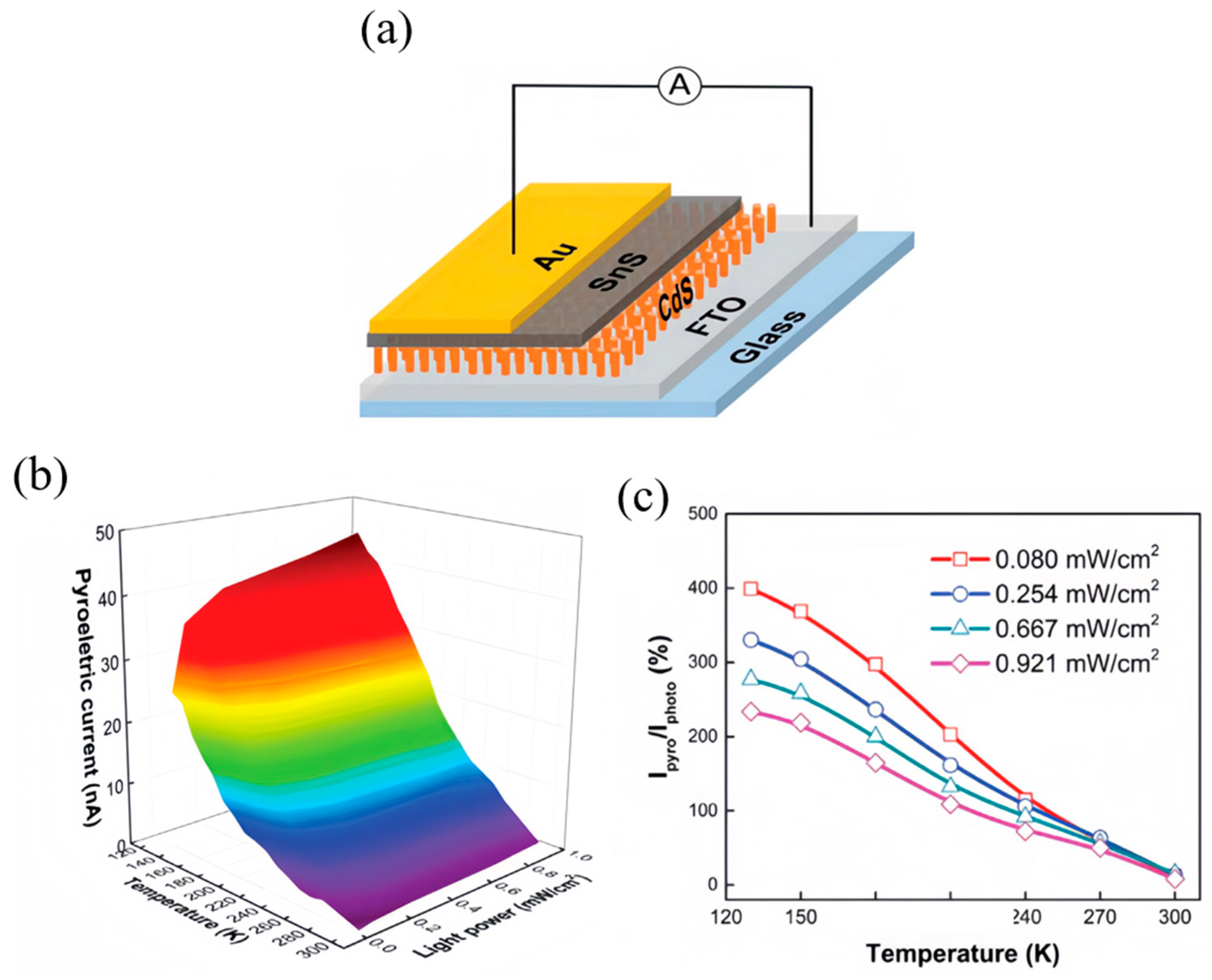
- Chang, Y.; Wang, J.; Wu, F.; Tian, W.; Zhai, W. Structural Design and Pyroelectric Property of SnS/CdS Heterojunctions Contrived for Low-Temperature Visible Photodetectors. Adv. Funct. Mater. 2020, 30, 2001450. [Google Scholar] [CrossRef]
- Zhang, M.; Hu, Q.; Ma, K.; Ding, Y.; Li, C. Pyroelectric effect in CdS nanorods decorated with a molecular Co-catalyst for hydrogen evolution. Nano Energy 2020, 73, 104810. [Google Scholar] [CrossRef]
- Lin, H.; Liu, H.; Qian, X.; Lai, S.-W.; Li, Y.; Chen, N.; Ouyang, C.; Che, C.-M.; Li, Y. Constructing a Blue Light Photodetector on Inorganic/Organic p–n Heterojunction Nanowire Arrays. Inorg. Chem. 2011, 50, 7749–7753. [Google Scholar] [CrossRef]
- Lin, H.; Liu, H.; Qian, X.; Chen, S.; Li, Y.; Li, Y. Synthesizing Axial Inserting p–n Heterojunction Nanowire Arrays for Realizing Synergistic Performance. Inorg. Chem. 2013, 52, 6969–6974. [Google Scholar] [CrossRef]
- Lin, H.; Jiang, A.; Xing, S.; Li, L.; Cheng, W.; Li, J.; Miao, W.; Zhou, X.; Tian, L. Advances in Self-Powered Ultraviolet Photodetectors Based on P-N Heterojunction Low-Dimensional Nanostructures. Nanomaterials 2022, 12, 910. [Google Scholar] [CrossRef] [PubMed]
- Lin, H.; Xing, S.; Jiang, A.; Li, M.; Chen, Q.; Wang, Z.; Jiang, L.; Li, H.; Wang, J.; Zhou, C. Controlled Synthesis of Large-Area Oriented ZnO Nanoarrays. Nanomaterials 2024, 14, 1028. [Google Scholar] [CrossRef] [PubMed]
- Rani, A.; Verma, A.; Singh, A.; Yadav, B.C. Monitoring of UV-A radiation by TiO2/CdS nanohybrid along with the high on-off ratio. Sens. Actuators A Phys. 2024, 367, 115060. [Google Scholar] [CrossRef]
- Vashishtha, P.; Abidi, I.H.; Giridhar, S.P.; Verma, A.K.; Prajapat, P.; Bhoriya, A.; Murdoch, B.J.; Tollerud, J.O.; Xu, C.; Davis, J.A.; et al. CVD-Grown Monolayer MoS2 and GaN Thin Film Heterostructure for a Self-Powered and Bidirectional Photodetector with an Extended Active Spectrum. ACS Appl. Mater. Interfaces 2024, 16, 31294–31303. [Google Scholar] [CrossRef] [PubMed]
- Krishnamurthi, V.; Khan, H.; Ahmed, T.; Zavabeti, A.; Tawfik, S.A.; Jain, S.K.; Spencer, M.J.S.; Balendhran, S.; Crozier, K.B.; Li, Z.; et al. Liquid-Metal Synthesized Ultrathin SnS Layers for High-Performance Broadband Photodetectors. Adv. Mater. 2020, 32, 2004247. [Google Scholar] [CrossRef]
- Tian, H.; Fan, C.; Liu, G.; Yuan, S.; Zhang, Y.; Wang, M.; Li, E. Ultrafast broadband photodetector based on SnS synthesized by hydrothermal method. Appl. Surf. Sci. 2019, 487, 1043–1048. [Google Scholar] [CrossRef]
- Patel, M.; Kim, J.; Kim, Y.K. Growth of Large-Area SnS Films with Oriented 2D SnS Layers for Energy-Efficient Broadband Optoelectronics. Adv. Funct. Mater. 2018, 28, 1804737. [Google Scholar] [CrossRef]
- Singh, P.; Rhee, D.; Baek, S.; Yoo, H.H.; Niu, J.; Jung, M.; Kang, J.; Lee, S. SnS/MoS2 van der Waals heterojunction for in-plane ferroelectric field-effect transistors with multibit memory and logic characteristics. EcoMat 2023, 5, e12333. [Google Scholar] [CrossRef]
- Ouyang, B.; He, W.; Wu, L.; Zhao, L.D.; Yang, Y. Thermo-phototronic effect in p-type Na-doped SnS single crystals for enhanced self-powered photodetectors. Nano Energy 2021, 88, 106268. [Google Scholar] [CrossRef]
- Zheng, D.; Fang, H.; Long, M.; Wu, F.; Wang, P.; Gong, F.; Wu, X.; Ho, J.C.; Liao, L.; Hu, W. High-Performance Near-Infrared Photodetectors Based on p-Type SnX (X = S, Se) Nanowires Grown via Chemical Vapor Deposition. ACS Nano 2018, 12, 7239–7245. [Google Scholar] [CrossRef]
- Chen, R.; Li, L.; Jiang, L.; Yu, X.; Zhu, D.; Xiong, Y.; Zheng, D.; Yang, W. Small-diameter p-type SnS nanowire photodetectors and phototransistors with low-noise and high-performance. Nanotechnology 2022, 33, 135707. [Google Scholar] [CrossRef] [PubMed]
- Fang, F.; Li, H.; Yao, H.; Jiang, K.; Liu, Z.; Lin, C.; Chen, F.; Wang, Y.; Liu, L. Two-Dimensional Hybrid Composites of SnS2 Nanosheets Array Film with Graphene for Enhanced Photoelectric Performance. Nanomaterials 2019, 9, 1122. [Google Scholar] [CrossRef]
- Zhang, L.; Wei, Z.; Wang, X.; Zhang, L.; Wang, Y.; Xie, C.; Han, T.; Li, F.; Luo, W.; Zhao, D.; et al. Ultrahigh-Sensitivity and Fast-Speed Solar-Blind Ultraviolet Photodetector Based on a Broken-Gap van der Waals Heterodiode. ACS Appl. Mater. Interfaces 2023, 15, 14513–14522. [Google Scholar] [CrossRef]
- Zhao, X.; Liu, S.; Zhang, H.; Chang, S.Y.; Huang, W.; Zhu, B.; Shen, Y.; Shen, C.; Wang, D.; Yang, Y.; et al. 20% Efficient Perovskite Solar Cells with 2D Electron Transporting Layer. Adv. Funct. Mater. 2018, 29, 1805168. [Google Scholar] [CrossRef]
- Kovacic, M.; Papac, J.; Kusic, H.; Karamanis, P.; Loncaric Bozic, A. Degradation of polar and non-polar pharmaceutical pollutants in water by solar assisted photocatalysis using hydrothermal TiO2-SnS2. Chem. Eng. J. 2020, 382, 122826. [Google Scholar] [CrossRef]
- Yu, J.; Suleiman, A.A.; Zheng, Z.; Zhou, X.; Zhai, T. Giant-Enhanced SnS2 Photodetectors with Broadband Response through Oxygen Plasma Treatment. Adv. Funct. Mater. 2020, 30, 2001650. [Google Scholar] [CrossRef]
- Zervos, M.; Mihailescu, C.N.; Giapintzakis, J.; Othonos, A.; Luculescu, C.R. Surface passivation and conversion of SnO2 to SnS2 nanowires. Mater. Sci. Eng. B 2015, 198, 10–13. [Google Scholar] [CrossRef]
- Zheng, D.; Wang, H.; Chen, R.; Li, L.; Guo, J.; Gu, Y.; Zubair, M.M.; Yu, X.; Jiang, L.; Zhu, D.; et al. High-detectivity tin disulfide nanowire photodetectors with manipulation of localized ferroelectric polarization field. Nanophotonics 2021, 10, 4637–4644. [Google Scholar] [CrossRef]
- Das, S.; Pal, S.; Larsson, K.; Mandal, D.; Giri, S.; Banerji, P.; Chandra, A.; Basori, R. Hydrothermally grown SnS2/Si nanowire core-shell heterostructure photodetector with excellent optoelectronic performances. Appl. Surf. Sci. 2023, 624, 157094. [Google Scholar] [CrossRef]
- Das, S.; Pal, S.; Mandal, D.; Banerji, P.; Chandra, A.; Basori, R. Enhanced Optoelectronic Performance of Silicon Nanowire/SnS2 Core-Shell Heterostructure With Defect Passivation in SnS2 by UV Treatment. IEEE Trans. Electron Devices 2023, 70, 4008–4013. [Google Scholar] [CrossRef]
- Das, S.; Sarkar, K.J.; Pal, B.; Mondal, H.; Pal, S.; Basori, R.; Banerji, P. SnS2/Si nanowire vertical heterostructure for high performance ultra-low power broadband photodetector with excellent detectivity. J. Appl. Phys. 2021, 129, 144671. [Google Scholar] [CrossRef]
- Kang, S.; Eshete, Y.A.; Lee, S.; Won, D.; Im, S.; Lee, S.; Cho, S.; Yang, H. Bandgap modulation in the two-dimensional core-shell-structured monolayers of WS2. iScience 2022, 25, 103563. [Google Scholar] [CrossRef] [PubMed]
- Gherabli, R.; Indukuri, S.R.K.C.; Zektzer, R.; Frydendahl, C.; Levy, U. MoSe2/WS2 heterojunction photodiode integrated with a silicon nitride waveguide for near infrared light detection with high responsivity. Light Sci. Appl. 2023, 12, 60. [Google Scholar] [CrossRef] [PubMed]
- Tan, H.; Fan, Y.; Zhou, Y.; Chen, Q.; Xu, W.; Warner, J.H. Ultrathin 2D Photodetectors Utilizing Chemical Vapor Deposition Grown WS2 With Graphene Electrodes. ACS Nano 2016, 10, 7866–7873. [Google Scholar] [CrossRef]
- Lin, Y.; Adilbekova, B.; Firdaus, Y.; Yengel, E.; Faber, H.; Sajjad, M.; Zheng, X.; Yarali, E.; Seitkhan, A.; Bakr, O.M.; et al. 17% Efficient Organic Solar Cells Based on Liquid Exfoliated WS2 as a Replacement for PEDOT:PSS. Adv. Mater. 2019, 31, 1902965. [Google Scholar] [CrossRef]
- Ghosh, S.; Brüser, V.; Kaplan-Ashiri, I.; Popovitz-Biro, R.; Peglow, S.; Martínez, J.I.; Alonso, J.A.; Zak, A. Cathodoluminescence in single and multiwall WS2 nanotubes: Evidence for quantum confinement and strain effect. Appl. Phys. Rev. 2020, 7, 041401. [Google Scholar] [CrossRef]
- Kumar, P.; Balakrishnan, V. Growth and microstructural evolution of WS2 nanostructures with tunable field and light modulated electrical transport. Appl. Surf. Sci. 2018, 436, 846–853. [Google Scholar] [CrossRef]
- Liu, F.; Zhou, H.; Gu, Y.; Dong, Z.; Yang, Y.; Wang, Z.; Zhang, T.; Wu, W. Solution Processed Photodetectors with PVK-WS2 Nanotube/Nanofullerene Organic–Inorganic Hybrid Films. ACS Appl. Mater. Interfaces 2022, 14, 43612–43620. [Google Scholar] [CrossRef] [PubMed]
- Chaudhary, N.; Khanuja, M. Architectural Design of Photodetector Based on 2D (MoS2 Nanosheets)/1D (WS2 Nanorods) Heterostructure Synthesized by Facile Hydrothermal Method. J. Electrochem. Soc. 2019, 166, B1276–B1285. [Google Scholar] [CrossRef]
- Gao, Y.; Du, Z.; Jiang, X.; Zheng, J.; Jiang, J.; Ye, S.; Zou, B.; Yang, T.; Zhao, J. Broadband MoS2 Square Nanotube-Based Photodetectors. ACS Appl. Nano Mater. 2023, 6, 7044–7054. [Google Scholar] [CrossRef]
- Li, X.; Wan, J.; Tang, Y.; Wang, C.; Zhang, Y.; Lv, D.; Guo, M.; Ma, Y.; Yang, Y. Boosting the UV–vis–NIR Photodetection Performance of MoS2 through the Cavity Enhancement Effect and Bulk Heterojunction Strategy. ACS Appl. Mater. Interfaces 2024, 16, 29003–29015. [Google Scholar] [CrossRef] [PubMed]
- Varshney, U.; Sharma, A.; Vashishtha, P.; Singh, P.; Gupta, G. Highly responsive self-driven broadband photodetector based on MoS2 nanorods/β-Ga2O3 heterojunction. Mater. Sci. Semicond. Process. 2023, 164, 107612. [Google Scholar] [CrossRef]
- Hafeez, M.; Gan, L.; Li, H.; Ma, Y.; Zhai, T. Large-Area Bilayer ReS2 Film/Multilayer ReS2 Flakes Synthesized by Chemical Vapor Deposition for High Performance Photodetectors. Adv. Funct. Mater. 2016, 26, 4551–4560. [Google Scholar] [CrossRef]
- An, Q.; Liu, Y.; Jiang, R.; Meng, X. Chemical vapor deposition growth of ReS2 nanowires for high-performance nanostructured photodetector. Nanoscale 2018, 10, 14976–14983. [Google Scholar] [CrossRef]
- Butanovs, E.; Butikova, J.; Zolotarjovs, A.; Polyakov, B. Towards metal chalcogenide nanowire-based colour-sensitive photodetectors. Opt. Mater. 2018, 75, 501–507. [Google Scholar] [CrossRef]
- Xie, X.; Shen, G. Single-crystalline In2S3nanowire-based flexible visible-light photodetectors with an ultra-high photoresponse. Nanoscale 2015, 7, 5046–5052. [Google Scholar] [CrossRef]
- Wang, T.; Jiang, T.; Meng, X. PVP-assisted synthesis of Sb2S3 nanowire for self-driven photodetector by using MXenes and Ag nanowires as electrodes. Appl. Nanosci. 2020, 10, 1845–1851. [Google Scholar] [CrossRef]
- Bera, A.; Das Mahapatra, A.; Mondal, S.; Basak, D. Sb2S3/Spiro-OMeTAD Inorganic–Organic Hybrid p–n Junction Diode for High Performance Self-Powered Photodetector. ACS Appl. Mater. Interfaces 2016, 8, 34506–34512. [Google Scholar] [CrossRef] [PubMed]
- Ismail, R.A.; Abeduljabbar, N.F.; Fatehi, M.W. Effect of dipping time on the properties of Sb2S3/Si heterojunction prepared by chemical bath deposition. Mater. Res. Express 2019, 6, 045915. [Google Scholar] [CrossRef]
- Wen, S.; Zhao, J.; Zhao, Y.; Xu, T.; Xu, J. Reduced graphene oxide (RGO) decorated Sb2S3 nanorods as anode material for sodium-ion batteries. Chem. Phys. Lett. 2019, 716, 171–176. [Google Scholar] [CrossRef]
- Kondrotas, R.; Chen, C.; Tang, J. Sb2S3 Solar Cells. Joule 2018, 2, 857–878. [Google Scholar] [CrossRef]
- Yu, Y.; Yan, W.; Wang, X.; Li, P.; Gao, W.; Zou, H.; Wu, S.; Ding, K. Surface Engineering for Extremely Enhanced Charge Separation and Photocatalytic Hydrogen Evolution on g-C3N4. Adv. Mater. 2018, 30, 1705060. [Google Scholar] [CrossRef]
- Nishikubo, R.; Li, S.; Saeki, A. Unprecedented Wavelength Dependence of an Antimony Chalcohalide Photovoltaic Device. Adv. Funct. Mater. 2022, 32, 2201577. [Google Scholar] [CrossRef]
- Zhong, M.; Wang, X.; Liu, S.; Li, B.; Huang, L.; Cui, Y.; Li, J.; Wei, Z. High-performance photodetectors based on Sb2S3 nanowires: Wavelength dependence and wide temperature range utilization. Nanoscale 2017, 9, 12364–12371. [Google Scholar] [CrossRef]
- Zhao, K.; Yang, J.; Zhong, M.; Gao, Q.; Wang, Y.; Wang, X.; Shen, W.; Hu, C.; Wang, K.; Shen, G.; et al. Direct Polarimetric Image Sensor and Wide Spectral Response Based on Quasi-1D Sb2S3 Nanowire. Adv. Funct. Mater. 2020, 31, 2006601. [Google Scholar] [CrossRef]
- Ye, K.; Wang, B.; Nie, A.; Zhai, K.; Wen, F.; Mu, C.; Zhao, Z.; Xiang, J.; Tian, Y.; Liu, Z. Broadband photodetector of high quality Sb2S3 nanowire grown by chemical vapor deposition. J. Mater. Sci. Technol. 2021, 75, 14–20. [Google Scholar] [CrossRef]
- Ma, Y.; Ma, C.; Yi, H.; Liang, H.; Wang, W.; Zheng, Z.; Zou, Y.; Deng, Z.; Yao, J.; Yang, G. 1D Sb2S3 with Strong Mie Resonance Toward Highly-Sensitive Polarization-Discriminating Photodetection and Its Application in High-Temperature-Proof Imaging and Dual-Channel Communications. Adv. Opt. Mater. 2023, 12, 2302039. [Google Scholar] [CrossRef]
- Liu, X.; Dong, S.; Zheng, X.; Zhang, Y.; Yao, Y.; Zhang, W.; Liu, Z.; Zhu, T.; Wang, H.E. Improving the optoelectronic properties of single-crystalline antimony sulfide rods through simultaneous defect suppression and surface cleaning. J. Mater. Chem. A 2023, 11, 8826–8835. [Google Scholar] [CrossRef]
- Zhang, J.; Hou, K.; Huang, T.; Yang, J.; Xu, B.; Li, S.; Yang, B.; Ma, W. Single-Crystal Sb2S3 Tube Prepared by Chemical Vapor Deposition for a 1 cm Photodetector Application. ACS Appl. Electron. Mater. 2022, 4, 2455–2462. [Google Scholar] [CrossRef]
- Chao, J.; Xing, S.; Zhang, J.; Qin, C.; Duan, D.; Wu, X.; Shen, Q. Synthesis of Sb2S3 nanowall arrays for high performance visible light photodetectors. Mater. Res. Bull. 2014, 57, 300–305. [Google Scholar] [CrossRef]
- Zhang, K.; Luo, T.; Chen, H.; Lou, Z.; Shen, G. Au-nanoparticles-decorated Sb2S3 nanowire-based flexible ultraviolet/visible photodetectors. J. Mater. Chem. C 2017, 5, 3330–3335. [Google Scholar] [CrossRef]
- Wang, J.; Qiao, Y.; Wang, T.; Yu, H.; Feng, Y.; Zhang, J. Isovalent bismuth ion-induced growth of highly-disperse Sb2S3 nanorods and their composite with p-CuSCN for self-powered photodetectors. CrystEngComm 2019, 21, 554–562. [Google Scholar] [CrossRef]
- Jiang, T.; Meng, X. Surface and Interface Engineering Enhanced Photodetector Based on Mo2C-C/Sb2S3 Composites. Nano 2021, 16, 2150004. [Google Scholar] [CrossRef]
- Shkir, M.; Alshahrani, T. Impact of Nd doping in Bi2S3 thin films coated by nebulizer spray pyrolysis technique for photodetector applications. Opt. Mater. 2023, 140, 113837. [Google Scholar] [CrossRef]
- Panwar, V.; Dey, M.; Sharma, P.; Sundar, K.; Nandi, S.; Tripathi, R.; Mondal, A.; Makineni, S.K.; Shukla, A.; Singh, A.; et al. Ultrahigh Photo-Responsivity and Detectivity in 2D Bismuth Sulfide Photodetector for Vis–NIR Radiation. Small 2024, 20, 2309428. [Google Scholar] [CrossRef]
- Rong, P.; Gao, S.; Ren, S.; Lu, H.; Yan, J.; Li, L.; Zhang, M.; Han, Y.; Jiao, S.; Wang, J. Large-Area Freestanding Bi2S3 Nanofibrous Membranes for Fast Photoresponse Flexible IR Imaging Photodetector. Adv. Funct. Mater. 2023, 33, 2300159. [Google Scholar] [CrossRef]
- Chitara, B.; Kolli, B.S.C.; Yan, F. Near-Infrared photodetectors based on 2D Bi2S3. Chem. Phys. Lett. 2022, 804, 139876. [Google Scholar] [CrossRef]
- Liu, Y.; Chen, P.; Dai, G.; Su, W.; Sun, Y.; Hou, J.; Zhang, N.; Zhao, G.; Fang, Y.; Dai, N. Single Bi2S3/Bi2S3-xOx nanowire photodetector with broadband response from ultraviolet to near-infrared range. Phys. E Low-Dimens. Syst. Nanostruct. 2020, 120, 114041. [Google Scholar] [CrossRef]
- Ding, T.; Tian, Y.; Dai, J.; Chen, C. Building one-dimensional Bi2S3 nanorods as enhanced photoresponding materials for photodetectors. Front. Optoelectron. 2015, 8, 282–288. [Google Scholar] [CrossRef]
- Yu, H.; Wang, J.; Wang, T.; Yu, H.; Yang, J.; Liu, G.; Qiao, G.; Yang, Q.; Cheng, X. Scalable colloidal synthesis of uniform Bi2S3nanorods as sensitive materials for visible-light photodetectors. CrystEngComm 2017, 19, 727–733. [Google Scholar] [CrossRef]
- Li, X.; Wu, Y.; Ying, H.; Xu, M.; Jin, C.; He, Z.; Zhang, Q.; Su, W.; Zhao, S. In situ physical examination of Bi2S3 nanowires with a microscope. J. Alloys Compd. 2019, 798, 628–634. [Google Scholar] [CrossRef]
- Wang, H.; Liu, R.; Zhang, S.; Wang, Y.; Luo, H.; Sun, X.; Ren, Y.; Lei, W. Controlled growth of high-quality Bi2S3 nanowires and their application in near-infrared photodetection. Opt. Mater. 2022, 134, 113174. [Google Scholar] [CrossRef]
- Yi, H.; Ma, C.; Wang, W.; Liang, H.; Cui, R.; Cao, W.; Yang, H.; Ma, Y.; Huang, W.; Zheng, Z.; et al. Quantum tailoring for polarization-discriminating Bi2S3 nanowire photodetectors and their multiplexing optical communication and imaging applications. Mater. Horiz. 2023, 10, 3369–3381. [Google Scholar] [CrossRef]
- Xu, X.; Fan, C.; Wang, Y.; Qi, Z.; Dai, B.; Jiang, H.; Wang, S.; Zhang, Q. In-plane Epitaxy of Bi2S3 Nanowire Arrays for Ultrasensitive NIR Photodetectors. Phys. Status Solidi (RRL) Rapid Res. Lett. 2020, 14, 2000384. [Google Scholar] [CrossRef]
- Maria, C.C.S.; Patil, R.A.; Hasibuan, D.P.; Saragih, C.S.; Lai, C.C.; Liou, Y.; Ma, Y.R. White-light photodetection enhancement and thin film impediment in Bi2S3 nanorods/thin-films homojunction photodetectors. Appl. Surf. Sci. 2022, 584, 152608. [Google Scholar] [CrossRef]
- Ghosh, K.; Giri, P.K. Experimental and theoretical study on the role of 2D Ti3C2Tx MXenes on superior charge transport and ultra-broadband photodetection in MXene/Bi2S3 nanorod composite through local Schottky junctions. Carbon 2024, 216, 118515. [Google Scholar] [CrossRef]
- Singh, A.; Chauhan, P.; Verma, A.; Yadav, B.C. Interfacial engineering enables polyaniline-decorated bismuth sulfide nanorods towards ultrafast metal–semiconductor-metal UV-Vis broad spectra photodetector. Adv. Compos. Hybrid Mater. 2024, 7, 88. [Google Scholar] [CrossRef]
- Devasia, S.; Shaji, S.; Avellaneda, D.A.; Aguilar Martinez, J.A.; Krishnan, B. In situ grown Bi2S3 nanorods in Cs3Bi2I9 thin films as broadband self-driven photodetector with improved photostability. Opt. Mater. 2024, 152, 115532. [Google Scholar] [CrossRef]
- Randle, M.; Lipatov, A.; Kumar, A.; Kwan, C.P.; Nathawat, J.; Barut, B.; Yin, S.; He, K.; Arabchigavkani, N.; Dixit, R.; et al. Gate-Controlled Metal–Insulator Transition in TiS3 Nanowire Field-Effect Transistors. ACS Nano 2018, 13, 803–811. [Google Scholar] [CrossRef]
- Liu, S.; Xiao, W.; Zhong, M.; Pan, L.; Wang, X.; Deng, H.X.; Liu, J.; Li, J.; Wei, Z. Highly polarization sensitive photodetectors based on quasi-1D titanium trisulfide (TiS3). Nanotechnology 2018, 29, 184002. [Google Scholar] [CrossRef] [PubMed]
- Ding, Y.; Xu, X.; Zhuang, Z.; Sang, Y.; Cui, M.; Li, W.; Yan, Y.; Tao, T.; Xu, W.; Ren, F.; et al. Self-powered MXene/GaN van der Waals Schottky ultraviolet photodetectors with exceptional responsivity and stability. Appl. Phys. Rev. 2024, 14, 041413. [Google Scholar] [CrossRef]
- Zhang, Y.; Chen, J.; Zhu, L.; Wang, Z.L. Self-Powered High-Responsivity Photodetectors Enhanced by the Pyro-Phototronic Effect Based on a BaTiO3/GaN Heterojunction. Nano Lett. 2021, 21, 8808–8816. [Google Scholar] [CrossRef]
- Gao, Z.; Chen, L.; Li, S.; Pan, X.; Liu, Y.; Gao, G.; Zou, B. Type-II CsPbBr3/ZnS Heterostructured Nanocrystals for High-Performance Self-Powered Photodetector. ACS Appl. Nano Mater. 2025, 8, 5623–5631. [Google Scholar] [CrossRef]
- Li, Z.; Li, H.; Jiang, K.; Ding, D.; Li, J.; Ma, C.; Jiang, S.; Wang, Y.; Anthopoulos, T.D.; Shi, Y. Self-Powered Perovskite/CdS Heterostructure Photodetectors. ACS Appl. Mater. Interfaces 2019, 11, 40204–40213. [Google Scholar] [CrossRef]
- Zhou, H.; Gui, P.; Yang, L.; Ye, C.; Xue, M.; Mei, J.; Song, Z.; Wang, H. High performance, self-powered ultraviolet photodetector based on a ZnO nanoarrays/GaN structure with a CdS insert layer. New J. Chem. 2017, 41, 4901–4907. [Google Scholar] [CrossRef]
- Xie, J.; Han, J.; Jiang, J.; Liu, L.; Fu, Z.; Wang, J. Self-Powered, Broadband, and Polarization-Sensitive Photodetector with Nb-WS2/Ta2NiSe5 Van der Waals Heterostructure. Adv. Opt. Mater. 2025, 13, 2403463. [Google Scholar] [CrossRef]
- Kumar, A.; Chakkar, A.G.; Das, C.; Kumar, P.; Sahu, S.; Saliba, M.; Kumar, M. Self-Powered Broadband Photodetectors Based on WS2-Anchored MoS2 with Enhanced Responsivity and Detectivity. Small 2025, 21, e2502900. [Google Scholar] [CrossRef]
- Zhou, C.; Liu, Q.; Fu, X.; Niu, W.; Wang, J.; Liu, X.; Zou, X.; Miao, J.; Shan, F.; Yang, Z. Self-Powered and Reconfigurable Double-Terminal MoS2 Photodetector for Image Recognition. Nano Lett. 2025, 25, 3515–3523. [Google Scholar] [CrossRef]
- Shen, M.; Wang, Q.; Liu, H.; Ye, H.; Yuan, X.; Zhang, Y.; Wei, B.; He, X.; Liu, K.; Cai, S.; et al. Self-Powered Polarization-Sensitive 3D Photodetector with Fast Response Enabled by Mechanically-Guided Assembly of Tubular MoS2/GaAs/InGaAs Heterostructure. Adv. Opt. Mater. 2025, 13, 2402848. [Google Scholar] [CrossRef]
- Deng, S.; Chen, Y.; Li, Q.; Sun, J.; Lei, Z.; Hu, P.; Liu, Z.-H.; He, X.; Ma, R. Direct growth of SnS2 nanowall photoanode for high responsivity self-powered photodetectors. Nanoscale 2022, 14, 14097–14105. [Google Scholar] [CrossRef]
- Kang, Y.; Deng, H.; Wu, K.; Wang, G.; Hong, J.; Wang, W.; Wu, J.; Zhou, H.; Xia, Y.; Cheng, S. Self-powered Sb2S3 photodetectors with efficient carrier transport enabled by compact vertical TiO2 nanorods. Opt. Lett. 2024, 49, 6533–6536. [Google Scholar] [CrossRef]
- Zamani, M.; Jamali-Sheini, F.; Cheraghizade, M. Visible-range and self-powered bilayer p-Si/n-Bi2S3 heterojunction photodetector: The effect of Au buffer layer on the optoelectronics performance. J. Alloys Compd. 2022, 905, 164119. [Google Scholar] [CrossRef]
- Yadav, S.M.; Pandey, A. 2D-SnS2 Nanoflakes Based Efficient Ultraviolet Photodetector. IEEE Trans. Nanotechnol. 2020, 19, 301–307. [Google Scholar] [CrossRef]
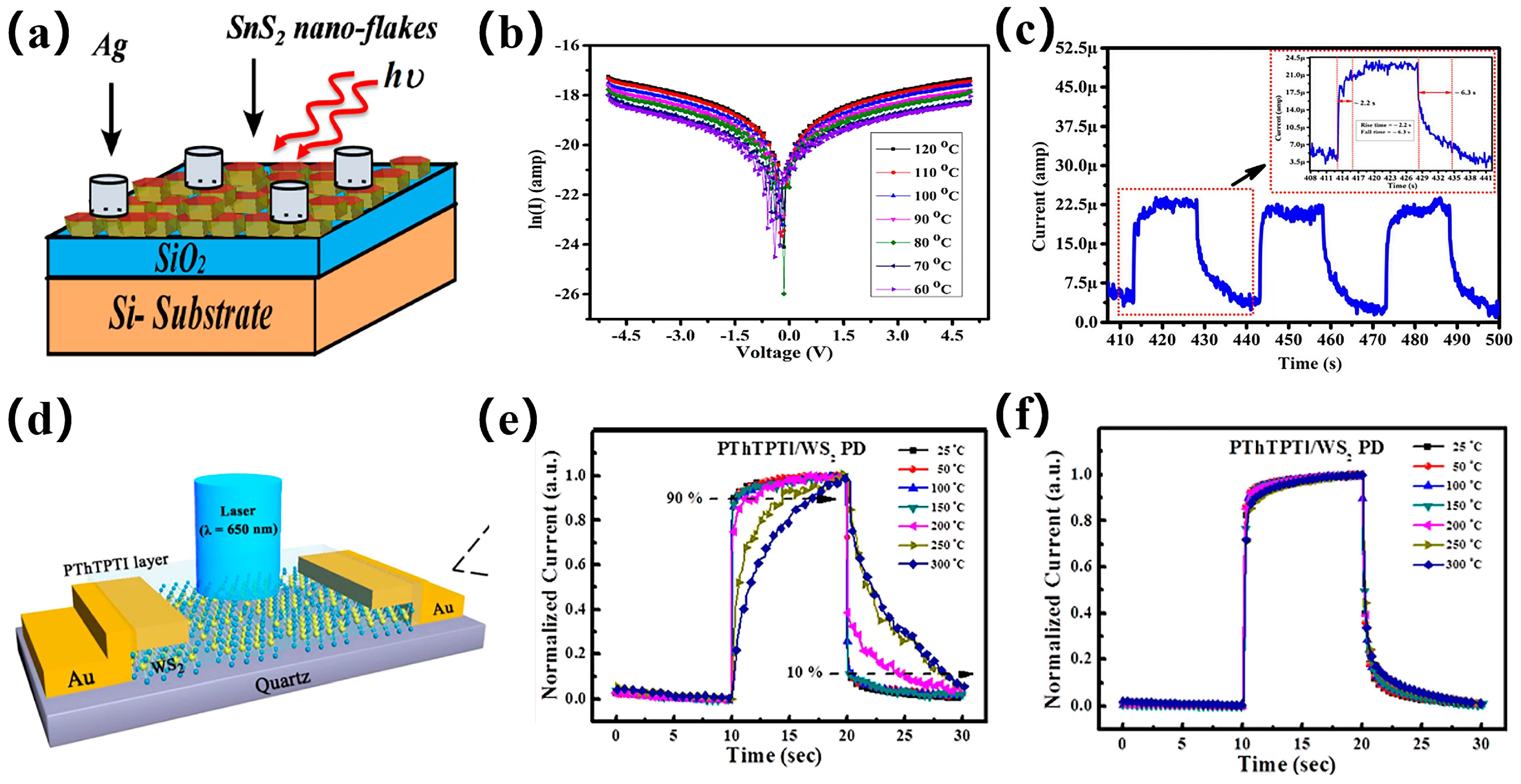
- Jin, Z.; He, D.; Zhou, Q.; Mao, P.; Ding, L.; Wang, J. Bilayer Heterostructured PThTPTI/WS2 Photodetectors with High Thermal Stability in Ambient Environment. ACS Appl. Mater. Interfaces 2016, 8, 33043–33050. [Google Scholar] [CrossRef]
- Vashishtha, P.; Prajapat, P.; Sharma, A.; Goswami, P.; Walia, S.; Gupta, G. Self-driven and thermally resilient highly responsive nano-fenced MoS2 based photodetector for near-infrared optical signal. Mater. Res. Bull. 2023, 164, 112260. [Google Scholar] [CrossRef]
- Wahalathantrige Don, R.; Das, P.; Ma, Z.; Kuruppu, U.M.; Feng, D.; Shook, B.; Gangishetty, M.K.; Stefan, M.C.; Pradhan, N.R.; Scott, C.N. Vinyl-Flanked Diketopyrrolopyrrole Polymer/MoS2 Hybrid for Donor–Acceptor Semiconductor Photodetection. Chem. Mater. 2023, 35, 4691–4704. [Google Scholar] [CrossRef]
- Li, Z.; Luo, J.; Hu, S.; Liu, Q.; Yu, W.; Lu, Y.; Liu, X. Strain enhancement for a MoS2-on-GaN photodetector with an Al2O3 stress liner grown by atomic layer deposition. Photonics Res. 2020, 8, 799–805. [Google Scholar] [CrossRef]
- Kaur, D.; Dahiya, R.; Sheokand, V.; Bassi, G.; Kumar, M. Ultrafast, self-powered and highly-stable PtS-Ga2O3 heterojunction photodetector for broad-spectrum sensing. Surf. Interfaces 2025, 61, 106125. [Google Scholar] [CrossRef]
- Xiong, L.; Zhang, L.; Lv, Q.; Li, T.; Song, W.; Si, J.; Zhu, W.; Wang, L. Amorphous gallium oxide (a-Ga2O3)-based high-temperature bendable solar-blind ultraviolet photodetector. Semicond. Sci. Technol. 2021, 36, 045010. [Google Scholar] [CrossRef]
- Zhang, M.; Liu, Z.; Yang, L.; Yao, J.; Chen, J.; Zhang, J.; Wei, W.; Guo, Y.; Tang, W. High-temperature reliability of all-oxide self-powered deep UV photodetector based on ϵ-Ga2O3/ZnO heterojunction. J. Phys. D Appl. Phys. 2022, 55, 375106. [Google Scholar] [CrossRef]
- Polyakov, A.Y.; Yun, J.H.; Usikov, A.S.; Yakimov, E.B.; Smirnov, N.B.; Shcherbachev, K.D.; Helava, H.; Makarov, Y.N.; Kurin, S.Y.; Shmidt, N.M.; et al. Structural, electrical and luminescent characteristics of ultraviolet light emitting structures grown by hydride vapor phase epitaxy. Mod. Electron. Mater. 2017, 3, 32–39. [Google Scholar] [CrossRef]
- Loser, S.; Valle, B.; Luck, K.A.; Song, C.K.; Ogien, G.; Hersam, M.C.; Singer, K.D.; Marks, T.J. High-Efficiency Inverted Polymer Photovoltaics via Spectrally Tuned Absorption Enhancement. Adv. Energy Mater. 2014, 4, 1301938. [Google Scholar] [CrossRef]
- Wang, X.F.; Zhao, H.M.; Shen, S.H.; Pang, Y.; Shao, P.-Z.; Li, Y.-T.; Deng, N.-Q.; Li, Y.-X.; Yang, Y.; Ren, T.-L. High performance photodetector based on Pd-single layer MoS2 Schottky junction. Appl. Phys. Lett. 2016, 109, 201904. [Google Scholar] [CrossRef]
- Yan, F.; Yang, X.; Liu, J.; Tang, H.; Tan, Y.A.; Li, Y. Optimizing the restoration performance of deduplication systems through an energy-saving data layout. Ann. Telecommun. 2019, 74, 461–471. [Google Scholar] [CrossRef]
- Ullah, S.; Bouich, A.; Ullah, H.; Mari, B.; Mollar, M. Comparative study of binary cadmium sulfide (CdS) and tin disulfide (SnS2) thin buffer layers. Sol. Energy 2020, 208, 637–642. [Google Scholar] [CrossRef]
- Wang, H.; Liu, Y.; Liu, H.; Chen, Z.; Xiong, P.; Xu, X.; Chen, F.; Li, K.; Duan, Y. Effect of various oxidants on reaction mechanisms, self-limiting natures and structural characteristics of Al2O3 films grown by atomic layer deposition. Adv. Mater. Interfaces 2018, 5, 1701248. [Google Scholar] [CrossRef]
- Zhang, Q.; Liu, H.; Guo, P.; Li, D.; Fan, P.; Zheng, W.; Zhu, X.; Jiang, Y.; Zhou, H.; Hu, W.; et al. Vapor growth and interfacial carrier dynamics of high-quality CdS-CdSSe-CdS axial nanowire heterostructures. Nano Energy 2017, 32, 28–35. [Google Scholar] [CrossRef]
- Kim, M.J.; Alvarez, S.; Chen, Z.; Fichthorn, K.A.; Wiley, B.J. Single-crystal electrochemistry reveals why metal nanowires grow. J. Am. Chem. Soc. 2018, 140, 14740–14746. [Google Scholar] [CrossRef] [PubMed]
- Zhang, T.; Liu, X.; Qu, G.; Lu, P.; Wang, J.; Wu, F.; Ren, Y. Secondary resource utilization of metallurgical solid waste: Current status and future prospects of wet extraction of valuable metals. Sep. Purif. Technol. 2024, 361, 131278. [Google Scholar] [CrossRef]
- Aung, T.; Giridhar, S.P.; Abidi, I.H.; Ahmed, T.; AI-Hourani, A.; Walia, S. Photoactive Monolayer MoS2 for Spiking Neural Networks Enabled Machine Vision Applications. Adv. Mater. Technol. 2025, 2401677. [Google Scholar] [CrossRef]
- Gogoi, K.; Chattopadhyay, A. Surface engineering of quantum dots for self-powered ultraviolet photodetection and information encryption. Langmuir 2022, 38, 2668–2676. [Google Scholar] [CrossRef] [PubMed]
- Li, Y.; Li, L.; Li, S.; Sun, J.; Fang, Y.; Deng, T. Highly sensitive photodetectors based on monolayer MoS2 field-effect transistors. ACS Omega 2022, 7, 13615–13621. [Google Scholar] [CrossRef] [PubMed]
- Li, J.; Li, Z.; Liu, X.; Li, C.; Zheng, Y.; Yeung, K.W.K.; Cui, Z.; Liang, Y.; Zhu, S.; Hu, W.; et al. Interfacial engineering of Bi2S3/Ti3C2Tx MXene based on work function for rapid photo-excited bacteria-killing. Nat. Commun. 2021, 12, 1224. [Google Scholar] [CrossRef]


| Electrode Material | Work Functions (eV) | Contact Type | I-V Curve Features | Ref. |
|---|---|---|---|---|
| Au | 5.1 | Schottky contact | Nonlinear | [74] |
| Cr | 4.5 | Ohmic contact | Linear | [75] |
| ITO | 4.4–4.5 | Quasi-Ohmic contact | Close to linear | [75] |
| Type of Contacts | Dark Current, nA (15 V) | Rejection Rate (15 V) | Responsivity, A W−1 (15 V) | Photo-Conductivity Gain (15 V) | Detectivity, cm W−1 HZ1/2 (15 V) |
|---|---|---|---|---|---|
| MSM, conventional Cr/Au | 0.71 | 5.4 × 10³ | 1.25 | ~14 | 8.3 × 10¹⁰ |
| MSM, interdigitated Cr/Au | 1.64 | 4.2 × 10³ | 2.23 | ~26 | 9.9 × 10¹⁰ |
| MSM, conventional Ni/Au | 0.59 | 4.1 × 10³ | 0.79 | ~9 | 5.8 × 10¹⁰ |
| MSM, interdigitated Ni/Au | 0.82 | 2.0 × 10⁴ | 5.40 | ~62 | 3.4 × 10¹¹ |
| MSM, hybrid Ni/Au and Ag-NW | 0.36 | 5.0 × 10³ | 0.58 | ~7 | 5.5 × 10¹⁰ |
| Material | Crystal Structure | Bandgap (eV) Direct- Indirect- | Type of Conductivity | Electrical Resistivity (Ω·cm) | Carrier Concentration (cm−3) | Carrier Mobility (cm2/v·s) | Ref. | |
|---|---|---|---|---|---|---|---|---|
| ZnS | Cubic | 3.7 | ~ | n-type | 1.79 × 10³ | 6.04 × 10¹⁹ | 90 | [91,92,93,94] |
| CdS | Hexagonal | 2.4 | ~ | n-type | 8.11 × 10⁻² | 2.96 × 10²⁰ | 14.5 | [95,96,97] |
| SnS | Orthorhombic | 1.32 | 1.09 | p-type | 5.4 × 10³ | 10 17 | 37.75 | [98,99,100] |
| WS2 | Hexagonal | 2.1 | 1.35 | n-type | 5 × 10⁴ | 1018~1019 | 50 | [101,102,103] |
| MoS2 | Hexagonal | 1.9 | 1.3 | n-type | 8.59 × 10⁴ | 1014~1015 | 0.5–17 | [104,105,106,107] |
| SnS2 | Trigonal | 2.9 | 2.1 | n-type | 1.2 × 10² | 5.43 × 10¹⁷ | 230 | [108,109] |
| ReS2 | Triclinic | 1.5 | ~ | n-type | 2~5 | 1019 | 16–30 | [110,111,112] |
| Sb2S3 | Orthorhombic | 1.78 | ~ | n-type | 1.3 × 10⁴ | 7.3 × 10¹³ | 6.4 | [113,114,115] |
| Bi2S3 | Orthorhombic | 1.3 | ~ | n-type | 7 × 10³ | 1017~1020 | ~ | [116,117,118] |
| In2S3 | Hexagonal | 2.0 | ~ | n-type | 38.8 | 3.8 × 10¹⁵ | 42.3 | [119,120] |
| TiS3 | Monoclinic | 1.1 | ~ | n-type | 2~6 | ~ | 80 | [121,122,123] |
| Material | Contact Electrodes | Methodology | Wavelength Power | Responsivity (A/W) | Detectivity (Jones) | EQE (%) | Rise Time Fall Time | Photo-I Dark-I | Ref. |
|---|---|---|---|---|---|---|---|---|---|
| ZnS NWs | Pt | TCVD | 365 nm 38 mW/cm2 | 2.761 | ~ | 0.572 | 3.2 s 3.6 s | ~ | [129] |
| ZnS NWs | Au | CVT | 325 nm 1.25 mW/cm2 | ~ | ~ | ~ | <0.1 s | ~ | [130] |
| ZnS NTs | Ag | Thermal Evaporation | ~ 40 mW/cm2 | 16.5 | 1.41 × 10⁹ | 8.92 | 0.12 s 0.4 s | 8.44 pA 1.32 μA | [131] |
| ZnS NTs | Ag | Thermal Evaporation | 297 nm 40 mW/cm2 | 2.56 | 1.67 × 10¹⁰ | 13.6 | 0.09 s 0.07 s | 14.9 pA 0.29 μA | [132] |
| ZnS NWA | Cr/Au | MOCVD | 325 nm 16 mW/cm2 | >1.87 | ~ | >710 | 5 ms 40 ms | ~ 508 pA | [133] |
| ZnS:Mn NRs | Ag | Hydrothermal | 310 nm 0.5 W/cm2 | 1.8 | ~ | 719 | 16 ms 1.1 ms | ~ | [134] |
| ZnS:Al NWs | ITO | Thermal Co-Evaporation | 254 nm 300 mW/cm2 | 3.1 × 10⁶ | ~ | 1.5 × 10⁷ | 153 s 445 s | ~ | [135] |
| ZnS/InP NWs | Cr/Au | CVD | 323 nm 1.87 μW/cm2 | 295 | 1.65 × 10¹³ | 1.10 × 10³ | 0.75 s 0.5 s | ~ 10.9 pA | [136] |
| ZnS/CdS NWs | Cr/Au | Thermal Evaporation | 450 nm 213 μW/cm2 | ~ | 2.23 × 10¹⁴ | ~ | 5 ms 7 ms | 10 fA 1200 pA | [137] |
| CdS NWs | Cr/Au | Vapor Transfer | 470 nm 0.93 mW/cm2 | ~ | 4.27 × 10¹² | ~ | 0.3 s 0.4 s | 4.7 fA 92.2 pA | [147] |
| CdS NWs | Cr/Au | CVD | 375 nm 0.01 mW/cm2 | 2.6 × 10⁵ | 2.3 × 10¹⁶ | 8.6 × 10⁵ | 12.6 ms 180 ms | 10−12 A 1.13 μA | [148] |
| CdS NRs | Ti/Au | CVD | 450 nm 0.5 mW/cm2 | 1.2 × 10⁴ | 2.8 × 10¹¹ | 3.5 × 10⁶ | 0.82 s 0.84 s | ~ | [149] |
| Sb/CdS NWs | Cr/Au | Two-Step CVD | 470 nm 19.1 μW/cm2 | 93.62 | 2.33 × 10¹⁴ | 2.47 × 10² | 0.384 s 0.312 s | 12.85 fA 45.5 pA | [150] |
| SnS/CdS NWA | Au | Hydrothermal-Thermal Evaporation | 650 nm 0.08 mW/cm2 | 10.4 m | 3.56 × 10¹¹ | ~ | <30 ms <30 ms | 14.9 pA 0.29 μA | [151] |
| Si/CdS NRs | Ag | Hydrothermal | ~ 2.55 mW/cm2 | 64.8 m | 1.31 × 10¹⁰ | ~ | 190.8 μs 298.4 μs | ~ | [139] |
| PPV/CdS NWA | Au | Electrochemical Co-Deposition | 545 nm 4.2 mW/cm2 | ~ | ~ | ~ | ~ | 0.027 μA 1.457 μA | [155] |
| TiO2/CdS NRs | Ag | Hydrothermal | 365 nm 40 μW/cm2 | 2.865 | 9.9 × 10¹² | 971.36 | 0.99 s 0.49 s | ~ | [157] |
| SnS NWs | Cr/Au | CVD | 838 nm 0.05 mW/cm2 | 1.6 × 10⁴ | 2.4 × 10¹² | ~ | 1.2 ms 15.1 ms | ~ | [164] |
| SnS NWs | Cr/Au | CVD | 830 nm 0.12 mW/cm2 | 2.6 × 10² | 1.8 × 10¹³ | ~ | 9.6 ms 14 ms | ~ | [165] |
| Material | Contact Electrodes | Methodology | Wavelength Power | Responsivity (A/W) | Detectivity (Jones) | EQE (%) | Rise Time Fall Time | Photo-I /Dark-I | Ref. |
|---|---|---|---|---|---|---|---|---|---|
| SnS2 NWs | Cr/Au | CVD | 520 nm 0.06 mW/cm2 | 2.1 × 10⁵ | 1.3 × 10¹⁶ | 4.0 × 10⁵ | 56 ms 91 ms | 3 × 10⁻¹³ A 2.74 μA | [172] |
| Si/SnS2 NWs | Au/Al | Hydrothermal | 340 nm 20 nW/cm2 | 383 | ~ | 1.3 × 10⁵ | 0.55 s 0.33 s | 2.9 × 10⁻¹² A ~ | [173] |
| WS2 NTs | Ti/Au | High temperature | 633 nm 532 W/cm2 | 2360 | ~ | 4.6 × 10⁶ | 256 μs 286 μs | 336 times lower | [54] |
| WS2 NTs- | Au | Solution synthesis | 552 nm 0.06 mW/cm2 | 0.2 m | 2.23 × 10⁴ | ~ | 0.92 s 0.09 s | ~ | [182] |
| MoS2/WS2 NRs | Ag | Hydrothermal | 785 nm 50 mW/cm2 | 15 μ | 24 × 106 | 16.9 × 10⁻⁶ | 0.82 s 1.59 s | ~ | [183] |
| MoS2 NTs | Ag | Hydrothermal | 915 nm 100 mW/cm2 | 2.33 m | 7.55 × 10⁸ | 3.33 × 10⁻¹ | 5.3 s 1.53 s | ~ 2 μA | [184] |
| Y-TiOPc/MoS2 NTs | Au | Anion exchange | 365–850 nm 0.01 mW/cm2 | 20,588 m | 1.94 × 10¹² | 494,736 | 134 ms 143 ms | ~ | [185] |
| β-Ga2O3/MoS2 NRs | Pt | Magnetron sputtering | 266 nm 30 μW/cm2 | 42.11 | 3.2 × 10¹¹ | 1.97 × 10⁴ | 0.29 s 0.3 s | 79 nA 16.92 μA | [186] |
| ReS2 NWs | Ag | CVD | 500 nm 0.42 nW/cm2 | 5.08 × 10⁵ | 6.1 × 10¹⁵ | 1.07 × 10⁶ | 1.8 s 3.9 s | 0.42 pA 4.95 nA | [188] |
| Material | Contact Electrodes | Methodology | Wavelength Power | Responsivity (A/W) | Detectivity (Jones) | EQE (%) | Rise Time Fall Time | Photo-I Dark-I | Ref. |
|---|---|---|---|---|---|---|---|---|---|
| In2S3 NWs | Cr/Au | NPT-CVT | 405 nm 2 W/cm2 | 16.01 | ~ | 4903 | ~ | 9.95 nA 112.4 μA | [189] |
| In2S3 NWs | Au/Ni | CVD | 450 nm 176.7 W/cm2 | 7.35 × 10⁴ | 2.4 × 10¹⁴ | 2.88 × 10⁷ | 6.5 ms 9.5 ms | 0.29 pA 293 nA | [190] |
| Sb2S3 NWs | Au | Steam Transport | 638 nm 0.03 mW/cm2 | 1152 | 2 × 10¹³ | ~ | 37 ms 38 ms | 2 × 10⁻¹⁰ A 4.2 × 10⁻⁸ A | [198] |
| Sb2S3 NWs | Au | Steam Transport | 450 nm 40 μW/cm2 | 343.4 m | ~ | ~ | 470 μs 680 μs | 69.6 times lower | [199] |
| Sb2S3 NWs | Ni/Au | CVD | 532 nm 0.03 mW/cm2 | 65 | 2.1 × 10¹⁴ | 1.5 × 10⁴ | 76 ms 83 ms | ~ 2.5 nA | [200] |
| Sb2S3 NWs | Ti/Au | APCVD | 635 nm 318 μW/cm2 | 270 | 4.37 × 10¹³ | 5.3 × 10⁴ | 10 ms 12 ms | 2800 times lower | [201] |
| Sb2S3 NRs | Au | Hydrothermal | 560 nm 0.38 mW/cm2 | 5.1 | 2.16 × 10¹⁰ | 1130.68 | 4.03 ms 4.08 ms | 109.8 times lower | [202] |
| Sb2S3 NTs | CVD | 808 nm 300 mW/cm2 | 8.5 m | 1.33 × 10⁶ | ~ | 22 ms 24 ms | 0.93 nA 185 nA | [203] | |
| Sb2S3 NWA | FTO | Polyol Reflux | 808 nm 640 mW/cm2 | ~ | ~ | ~ | 0.52 s 1.1 s | 7.4 nA 113.5 nA | [204] |
| Au:Sb2S3 NWs | Cr/Au | CVD | 600 nm 680 μW/cm2 | 59.5 | 4.29 × 10¹⁰ | ~ | 0.2 s 0.3 s | 57 pA 163 nA | [205] |
| CuSCN/Sb2S3 NRs | ITO | Two-Step Hydrothermal | 600 nm 680 μW/cm2 | ~ | ~ | ~ | 0.18 s 0.15 s | 102 times lower | [206] |
| Mo2C-C/Sb2S3 NRs | Au | Hydrothermal | 400 nm 320 W/cm2 | ~ | ~ | ~ | 52.7 ms 79.2 ms | 150 times lower | [207] |
| Bi2S3 NRs | Au | One-Pot Hydrothermal | ~ | ~ | ~ | ~ | 371.6 ms 386 ms | 102 times lower | [213] |
| Bi2S3 NRs | ITO | Colloidal Chemical | 650 nm 4.1 mW/cm2 | ~ | ~ | ~ | 0.3 s 0.6 s | 10 times lower | [214] |
| Bi2S3 NWs | Cr/Au | CVD | 700 nm 1.54 mW/cm2 | 3.57 | ~ | 633 | 0.1 0.1 | ~ | [215] |
| Bi2S3 NWs | Pt | CVD | 830 nm 52 mW/cm2 | 4.21 | 1.64 × 10¹⁰ | 981.76 | 12.25 ms 12.25 ms | ~ | [216] |
| Bi2S3 NWs | Ti/Au | APCVD | 532 nm 23.8 μW/cm2 | 23,760 | 3.68 × 10¹³ | 5.5 × 10⁶ | 1 ms 4.5 ms | ~ | [217] |
| Bi2S3 NRA | Au | PVD | 830 nm 64 nW/cm2 | 5233 | 1.8 × 10¹² | 7.8 × 10³ | 21 μs 7.8 ms | ~ | [218] |
| Bi2S3 NRA | Ta | Hot Plate PVD | ~ 22.7 W/cm2 | 749.6 | 5.61 × 10⁸ | ~ | 192 ms 270 ms | 0.96 μA 4.5 μA | [219] |
| Ti3C2Tx/Bi2S3 NRs | Au | In Situ Hydrothermal | 808 nm 0.03 mW/cm2 | 2.55 × 10⁻² | 3.9 × 10¹² | 3.9 × 10³ | 0.3 ms 2.1 ms | 255 times lower | [220] |
| Bi2S3/PANI NRs | Ag | Hydrothermal | 365 nm 50 μW/cm2 | 26,760 | 5.24 × 10¹³ | 9073 | 50 ms 60 ms | 0.003 μA 0.58 μA | [221] |
| Cs3Bi2I9:Bi2S3 NRs | Ag/C | USD | 532 nm 790 μW/cm2 | 0.59 × 10⁻³ | 8.18 × 10⁹ | 198 | ~ | 0.68 nA 1.35 nA | [222] |
| Material | Contact Electrodes | Methodology | Wavelength Power | Responsivity (A/W) | Detectivity (Jones) | EQE (%) | Rise Time Fall Time | Ref. |
|---|---|---|---|---|---|---|---|---|
| CsPbBr3/ZnS | Al/ITO | Hot injection and spin coating | 365 nm 2 mW/cm2 | 37.5 m | 1.21 × 10¹² | ~ | 150 ms 30 ms | [227] |
| MAPbI3/CdS | Au/ITO | CBD | 325 nm 10 mW/cm2 | 0.43 | 2.3 × 10¹¹ | ~ | 3.2 ms 9.6 ms | [228] |
| ZnO/CdS/GaN | In/ITO | ~ | 300 nm 0.61 mW/cm2 | 176 m | 1012 | 719 | <0.35 s <0.35 s | [229] |
| Nb-WS2/Ta2NiSe5 | Au | Mechanical exfoliation and dry transfer techniques | 660 nm 0.45 mW/cm2 | 57.64 | 6 × 10¹⁰ | 10,854 | 118 μs 13 μs | [230] |
| MoS2/WS2 | Au/Cr | Spin coating and CVD | 580 nm 120 μW/cm2 | 282 m | ~ | 60.59 | 375 μs 6 ms | [231] |
| Ag-MoS2 | Pt | Ar plasma | 532 nm 0.519 W/cm2 | 280 m | 0.76 × 10¹¹ | 65 | 224 μs 293 μs | [232] |
| MoS2/GaN | Au/Ni | Vapor transfer | UV 0.93 mW/cm2 | 631 m | 8.5 × 10¹⁰ | 214 | 1.04 ms 0.8 ms | [158] |
| MoS2/GaAs/InGaAs | Au/Ni | MBE | 650 nm 3.48 mW/cm2 | 86 m | 2.3 × 10¹⁶ | 16 | 12.6 ms 18 ms | [233] |
| SnS2 | FTO | Hydrothermal | 475 nm 10 mW/cm2 | 1460 μ | ~ | ~ | ~ | [234] |
| TiO2/Sb2S3 | FTO/Au | Hydrothermal and spin coating | 625 nm 9 W/cm2 | 0.29 | 3.37 × 10¹² | ·~ | 9.3µs 7.8µs | [235] |
| p-Si/Bi2S3 | Au | CVD | Red ~ | 0.94 m | 8.92 × 10⁸ | 29,685 | ~ | [236] |
| Material | Contact Electrodes | Methodology | Operating Temperature (℃) | Responsivity (A/W) | Detectivity (Jones) | EQE (%) | Rise Time Fall Time | Ref. |
|---|---|---|---|---|---|---|---|---|
| SnS2 | Ag | Solvothermal method | 120 | 5.5 | 1.72 × 10¹³ | 1868 | 2.2 s 6.3 s | [237] |
| PThTPTI/WS2 | Au | CVD | 300 | ~ | ~ | ~ | 6.89 ms 8.43 ms | [238] |
| MoS2 | Pt | RF sputtering technology | 100 | 1170 m | 1.6 × 10¹⁰ | 409 | ~ | [239] |
| MoS2/GaN | Au | Vapor transfer | 100 | 631 m | 8.5 × 10¹⁰ | 214 | 1.04 ms 0.8 ms | [158] |
| PDPPVTT/MoS2 | Au/Cr | CVT | ~ | ~ | ~ | ~ | ~ | [240] |
| MoS2/GaN/Al2O3 | Au/Cr | CVD and ALD | ~ | 24.62 | ~ | 8381 | ~ | [241] |
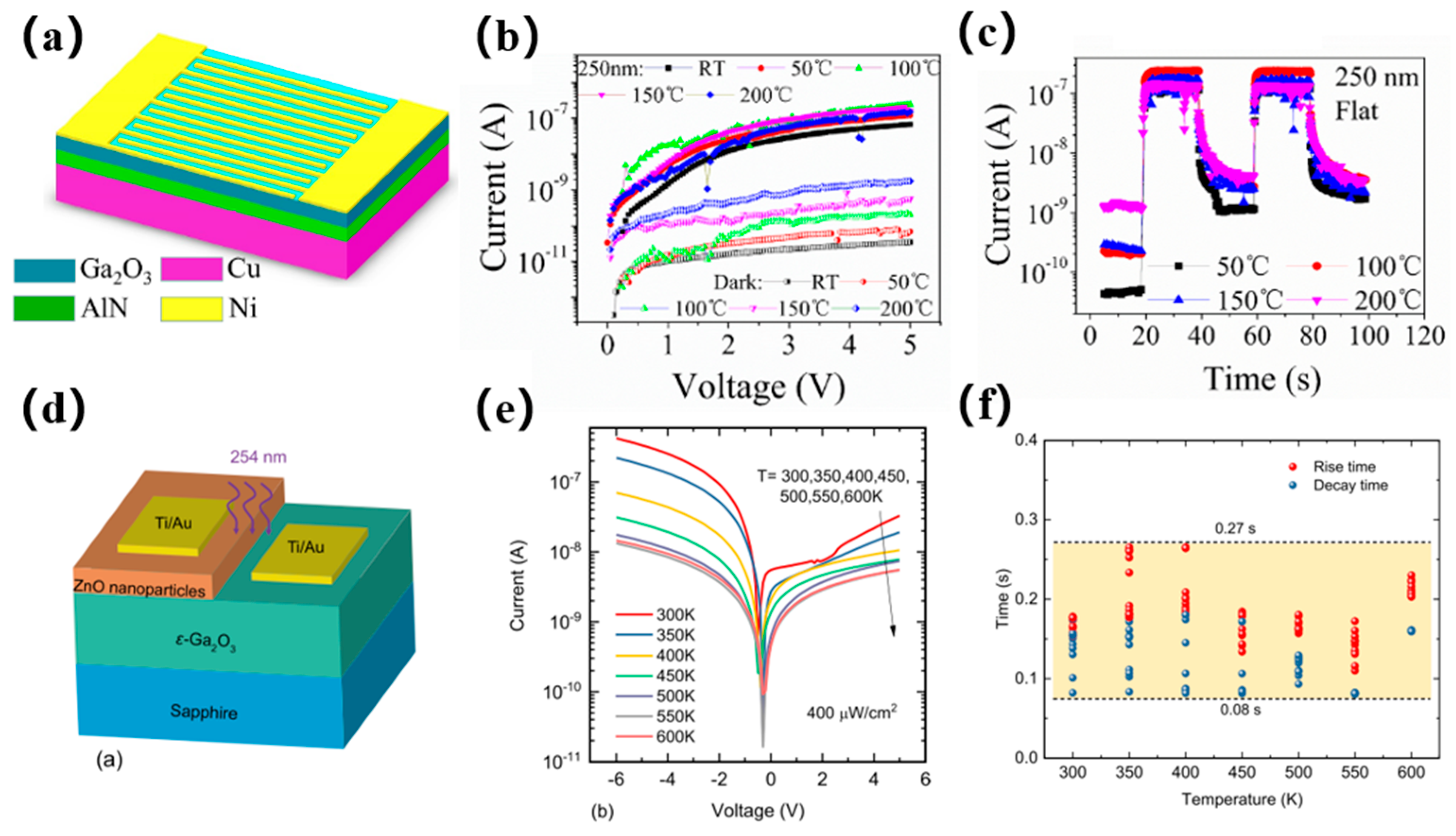
| Ga2O3 | Au/Ni | CVD | 200 | 0.518 | ~ | ~ | ~ | [243] |
| ε-Ga2 O3/ZnO | Ti/Au | CVD | >500 K | 2.4 m | 5 | 1.5 | ~ | [244] |
Disclaimer/Publisher’s Note: The statements, opinions and data contained in all publications are solely those of the individual author(s) and contributor(s) and not of MDPI and/or the editor(s). MDPI and/or the editor(s) disclaim responsibility for any injury to people or property resulting from any ideas, methods, instructions or products referred to in the content. |
© 2025 by the authors. Licensee MDPI, Basel, Switzerland. This article is an open access article distributed under the terms and conditions of the Creative Commons Attribution (CC BY) license (https://creativecommons.org/licenses/by/4.0/).
Share and Cite
Chen, J.; Li, M.; Lin, H.; Zhou, C.; Chen, W.; Wang, Z.; Li, H. Advances in One-Dimensional Metal Sulfide Nanostructure-Based Photodetectors with Different Compositions. J. Compos. Sci. 2025, 9, 262. https://doi.org/10.3390/jcs9060262
Chen J, Li M, Lin H, Zhou C, Chen W, Wang Z, Li H. Advances in One-Dimensional Metal Sulfide Nanostructure-Based Photodetectors with Different Compositions. Journal of Composites Science. 2025; 9(6):262. https://doi.org/10.3390/jcs9060262
Chicago/Turabian StyleChen, Jing, Mingxuan Li, Haowei Lin, Chenchen Zhou, Wenbo Chen, Zhenling Wang, and Huiying Li. 2025. "Advances in One-Dimensional Metal Sulfide Nanostructure-Based Photodetectors with Different Compositions" Journal of Composites Science 9, no. 6: 262. https://doi.org/10.3390/jcs9060262
APA StyleChen, J., Li, M., Lin, H., Zhou, C., Chen, W., Wang, Z., & Li, H. (2025). Advances in One-Dimensional Metal Sulfide Nanostructure-Based Photodetectors with Different Compositions. Journal of Composites Science, 9(6), 262. https://doi.org/10.3390/jcs9060262