Article

Features of the Process of Surface Preparation of Products Using Glow Discharge Plasma During the Deposition of Modifying Coatings

1
Department of High-Efficiency Machining Technologies, Moscow State University of Technology «STANKIN», Vadkovsky per. 1, Moscow 127055, Russia
2
Institute of Design and Technological Informatics of the Russian Academy of Sciences (IDTI RAS), Vadkovsky per. 18-1a, Moscow 127994, Russia
3
Materials Science and Metallurgy Shared Use Research and Development Center, National University of Science and Technology «MISiS», Leninsky Prospect 4, Moscow 119049, Russia
4
Joint-Stock Company «Central Research Institute of Mechanical Engineering» (JSC «TsNIIMash»), Pionerskaya Street, Building 4, Korolev 141070, Moscow Region, Russia
*
Author to whom correspondence should be addressed.
J. Compos. Sci. 2025, 9(12), 640; https://doi.org/10.3390/jcs9120640 (registering DOI)
Submission received: 18 October 2025 / Revised: 8 November 2025 / Accepted: 19 November 2025 / Published: 22 November 2025
(This article belongs to the Section Composites Manufacturing and Processing)

Abstract

The deposition characteristics of coatings on a titanium alloy substrate were compared using two alternative surface preparation methods: Hollow Cathode Spaces (HCSs) and Ion Bombardment (IB). After deposition of ZrN coatings, the wear resistance of the samples increased by 50–70% compared to uncoated samples, while the HCS method provided 30% higher wear resistance than the IB method. Coated samples deposited using the HCS and IB methods demonstrated very similar friction coefficient values, with a slight (10–15%) decrease in this parameter for the HCS samples. Varying the bias voltage on the substrate (−900, −1200, and −1500 V) when using the HCS method significantly affected wear resistance. The calculated optimal value of the bias voltage when using the HCS method is −1126 V. During the pre-treatment of the substrate using the HCS and IB methods, a transition layer can be formed in the area of the coating–substrate interface; the thickness of this layer varies within the range of 15–400 nm, and the composition is a mixture of coating (zirconium) and substrate (titanium, aluminum, and vanadium) materials.

1. Introduction

The efficiency of cleaning and thermal activation of the substrate surface largely determines the reliability and durability of physical vapor deposition (PVD) coatings [1,2,3,4,5,6,7,8]. Various methods are used for cleaning and thermal activation of the substrate surface in a vacuum chamber, including the use of infrared heaters [2,4,9], as well as laser irradiation [10,11,12]. However, these methods require additional equipment and technological operations, which complicates the already complex process of coating deposition. For cleaning and thermal activation of the surface of products before coating deposition, the most commonly used methods are ion cleaning (ion etching) and heating by bombardment with accelerated ions [3,4,6,8,13,14,15,16,17,18]. Such treatment not only allows for cleaning the surface of residual microcontaminants and heating it to the required temperature but also reduces surface microdefects and creates a favorable microrelief [5,9,10,11]. All of the above allows for achieving a high strength of adhesive bonds between the substrate and the coating [6,7,18]. The principle of ion etching is that bombarding ions, upon falling on the substrate surface, transfer their kinetic energy to its atoms, as a result of which atoms with the lowest binding energy with the substrate (e.g., contaminant atoms) are emitted from the substrate surface [1,19]. In this case, the main part of the ion energy is dissipated in the surface layer of the substrate as heat [20,21]. At relatively low ion energies, a layer of the corresponding metal is formed on the substrate surface; with increasing energy, the sputtering process intensifies, and when the energy value ≥104 eV is reached, the process of ion penetration into the surface layers of the substrate begins [10,21,22]. The parameters of the ion etching process depend on the ion energy, ion flux density, treatment duration, ion mass, their angle of incidence, and the substrate material and the state of its surface [10,20,23,24,25,26,27].
The vacuum arc method enables etching with both metal ions and gas ions in combination with metal ions [18,28]. This method allows for wide-range control of the bombarding ion energy by varying the negative bias potential on the substrate, typically from 200 to 1500 V [21,29].
Bombardment with metal ions not only ensures an atomically clean substrate surface but also the formation of implantation zones, which further enhance the adhesive bonds between the coating and the substrate [30,31].
A problem with metal ion etching of arc evaporators is the uneven distribution of ion current density across the plasma flow cross-section [5,26,32]. Repeated cross-deposition of sputtered contaminants onto the substrate can also occur [33,34,35,36].
An alternative to ion etching is ion cleaning in a self-sustaining stationary glow discharge plasma. This method is based on the acceleration of gas plasma ions onto the surface of the substrate being processed, which serves either as the cathode of the glow discharge itself or as an additional electrode negative with respect to the plasma [1,3,17,33,34,35]. Ion processing in a glow discharge significantly improves the adhesion of the coating to the substrate and reduces the porosity of the deposited coating [37,38,39,40]. It should be taken into account that an irregular distribution of the electric field strength over the surface of the substrate being processed can lead to uneven heating of individual areas [41,42]. To eliminate this drawback, various glow discharge implementation schemes are used, for example, using the hollow cathode effect. In this case, the cathode requires a closed or quasi-closed equipotential cavity, within which the discharge is localized due to the emitted electrons oscillating within the cavity, repeatedly reflecting off the walls. Due to this, the time of their active contact increases, significantly increasing the degree of gas ionization and the density of the glow discharge plasma within the hollow cathode [43]. One effective and easy-to-implement method of using glow discharge for cleaning and thermally activating the surfaces of products before coating deposition is the Hollow Cathode Space (HCS) method [44].
Titanium alloy 6Al-4V (Grade 5) is one of the most common titanium alloys [45,46,47]. Its applications include aircraft construction, medicine (various implants), energy (including nuclear), and a number of other fields. This alloy contains aluminum, which positively affects the heat resistance and strength of components, and vanadium, which contributes to increased strength and ductility. The elemental composition of titanium alloy 6Al-4V is presented in Table 1.
The 6Al-4V alloy boasts high strength, low hydrogen sensitivity, and good corrosion resistance, making it ideal for use in mechanical engineering and power generation. The relatively low specific gravity of this alloy, combined with its high strength, means it is widely used in the aviation industry.
In this study, a method for heating and cleaning the surface of workpieces using a glow discharge was used to implement the Hollow Cathode Spaces (HCSs) [44]. The hollow cathode effect is achieved through the specific arrangement of the workpieces, which are positioned in a vacuum chamber on a rotary table. Their surfaces form a partially enclosed internal region—the quasi-cavity of the hollow cathode. The objective was to compare the HCS method with traditional Ion Bombardment, as well as to investigate the optimal parameters for the HCS method.
To eliminate the influence of additional factors on the study results, a coating of a simple two-component composition ZrN was deposited. This coating exhibits good performance properties [49,50,51,52,53], while its composition is unmatched by the substrate, allowing for a more accurate study of diffusion processes.

2. Materials and Methods

The samples were pre-annealed (700–800 °C followed by air cooling) to relieve residual stress and obtain an optimal combination of strength and ductility.
Experiments were conducted on a modernized VIT-2 setup (IDTI RAS-MSUT «STANKIN», Moscow, Russia) [54,55,56,57]. This setup utilizes two types of evaporators: First, there is a filtered cathodic vacuum arc deposition (FCVAD) system [58,59,60], which provides up to 98% separation of microparticles while maintaining a high degree of plasma flow focusing. The second type of evaporator, the Controlled Accelerated Arc Deposition (CAA-PVD) system [28], is characterized by high energy efficiency and a reduced microparticle content compared to traditional arc-type evaporators. A negative voltage from a 30 kW high-voltage source is applied to a rotary table located inside the vacuum chamber. The set voltage range is from 0 to −1500 V, and the permissible current is 30 A. All walls of the vacuum chamber serve as anodes. A Zr cathode (99.8%) was mounted on the evaporators of the CAA-PVD system. The coating thickness is 3.0 ± 0.2 µm.
The process is carried out at a gas pressure of 13 to 1300 Pa and a surface temperature of 500–600 °C. The voltage is maintained constant between 400 and 1000 V. The temperature of the parts depends significantly on the working gas pressure and the cathode voltage. At vacuum chamber pressures below 130 Pa, the ion volume density is insufficient to achieve the required surface temperature.
Two alternative surface preparation processes before coating deposition were compared:
  • Hollow Cathode Spaces (HCSs).
  • Ion Bombardment (IB).

2.1. Hollow Cathode Spaces (HCSs)

Cleaning and heating are performed in a glow discharge plasma at a pressure of 5.0 Pa. Parts in a vacuum chamber form Hollow Cathode Spaces. Argon (Ar) is used as the working gas. Initially, for the HCS cleaning and heating processes, a minimum voltage is applied to the turntable, at which the glow discharge begins (approximately −100 V). As the microarcs disappear, the voltage increases until the sample temperature reaches 650 °C. Ion cleaning and heating occur by bombarding the surface (glow discharge cathode) with positively charged gas ions accelerated in the cathode layer of the discharge. A detailed description of the processes of cleaning and thermal activation of the surface using the HCS method is contained in [44].

2.2. Ion Bombardment (IB)

Arc evaporators are switched on to generate metal plasma, and the arc-burning current on all evaporators is 90 A. The pressure in the working chamber is not higher than 0.005 Pa. A negative voltage of −100 V from a high-voltage power source is applied to the rotary table with the parts fixed on it. As the heating proceeds and the probability of microarcs decreases, the voltage gradually increases until the surface temperature of the parts reaches 650 °C.
To study the effect of HCS process parameters (bias voltage) on the wear resistance of coated specimens, three deposition processes were conducted. Table 2 shows the specimen designations based on the substrate bias voltage used in the HCS process. The remaining parameters were held constant for all three deposition processes. Specimens with different HCS process parameters, as well as a specimen prepared using the IB method, were compared.
Scratch testing was performed using a Nanovea scratch tester (Nanovea, Irvine, CA, USA) in accordance with ASTM C 1624 [61] over a load range of 0–40 N using a conical diamond indenter with an angle of 120° and a radius of 100 μm. Three measurements were taken for each type of coating, after which the average value and the range of values were deter-mined.
A DUCOM POD-4.0 (Ducom Instruments Pvt. Ltd., Bangalore, India) universal tribometer was used to conduct friction and wear tests using a pin-on-disk/ball-on-disk system. The loading scheme used in this device ensured that the working fluid (ball) load was set independently of the friction console, which reduced vibrations in the system and increased the accuracy of the tests. The load was 10 N, and the rotation speed was 100 rpm. The furrow radius was 10–12 mm. The linear velocity of the indenter movement along the sample is approximately 0.125 m/s (may vary slightly with changes in the track diameter). The tests were conducted over 30,000 s (about 8½ h), using an indenter (ball) made of ASTM 52,100 bearing steel, the properties of which are similar to those of the sample material. The wear resistance was determined according to ASTM G99 [62]. The testing was conducted at room temperature and without any lubricant. The wear results are presented as the volume loss in cubic millimeters for the test sample (coated disk) and as the mass loss for the ball. Three measurements were taken for each type of coating, after which the average value and the range of values were determined.
A JEM 2100 transmission electron microscope (TEM) (JEOL, Akishima, Japan) at an accelerating voltage of 200 kV was used to examine the micro- and nanostructures. The TEM, equipped with an energy-dispersive X-ray system (INCA Energy, Oxford Instruments, High Wycombe, UK), was employed to analyze the coating composition. Lamellas were made on a Strata focused ion beam 205 (FEI, Hillsboro, OR, USA). There are a number of methods for preparing TEM samples using FIB methods. The most universal method is the production of cross-section lamellas with subsequent fixation on a TEM grid and cutting out a thin window (cross-section lift-out TEM lamella). All manipulations are carried out in the microscope column.
The microstructures of the surfaces of the obtained samples were studied using an FEI Quanta 600 FEG scanning electron microscope (SEM) (Materials & Structural Analysis Division, Hillsboro, OR, USA) with a field emission cathode and an integrated attachment of an EDAX energy-dispersive X-ray microanalyzer.

3. Results

3.1. Comparison of the Effectiveness of Using HCS and IB Methods

A study of the surface roughness of the samples before and after coating deposition showed that the roughness of the coated samples was significantly lower than that of the uncoated samples. This may be due to the effect of leveling surface defects and surface smoothing during coating deposition [63]. A comparison of the surface roughness of the HCS and IB samples shows that the HCS method provides a slightly lower surface roughness of the coating (Table 3), which may be due to the lower surface roughness of the substrate prepared using this method.
The results of the pin-on-disk wear resistance study for titanium alloy specimens coated with Ion Bombardment (IB, green line) and glow discharge (HCS, blue line) coatings, as well as without coating (red line), are shown in Figure 1a. After coating deposition, the wear resistance of the specimens increased by 50–70% compared to uncoated specimens, while the use of the HCS method ensures wear resistance that is 20% higher than that of the IB method.
Studies of the friction coefficient (Figure 1b) show that coating deposition reduces this parameter from 0.5 to 0.3 (a 65% reduction). Moreover, coating samples deposited using the HCS and IB methods exhibit very similar friction coefficient values, with a slight (10–15%) reduction for the HCS samples. Thus, the use of the IB or HCS methods significantly affects the wear resistance of the coating, but only slightly affects the tribological parameters. The effect on the tribological properties of the samples may be primarily due to differences in the substrate surface roughness after pretreatment, which, accordingly, affects the final surface roughness after coating deposition.
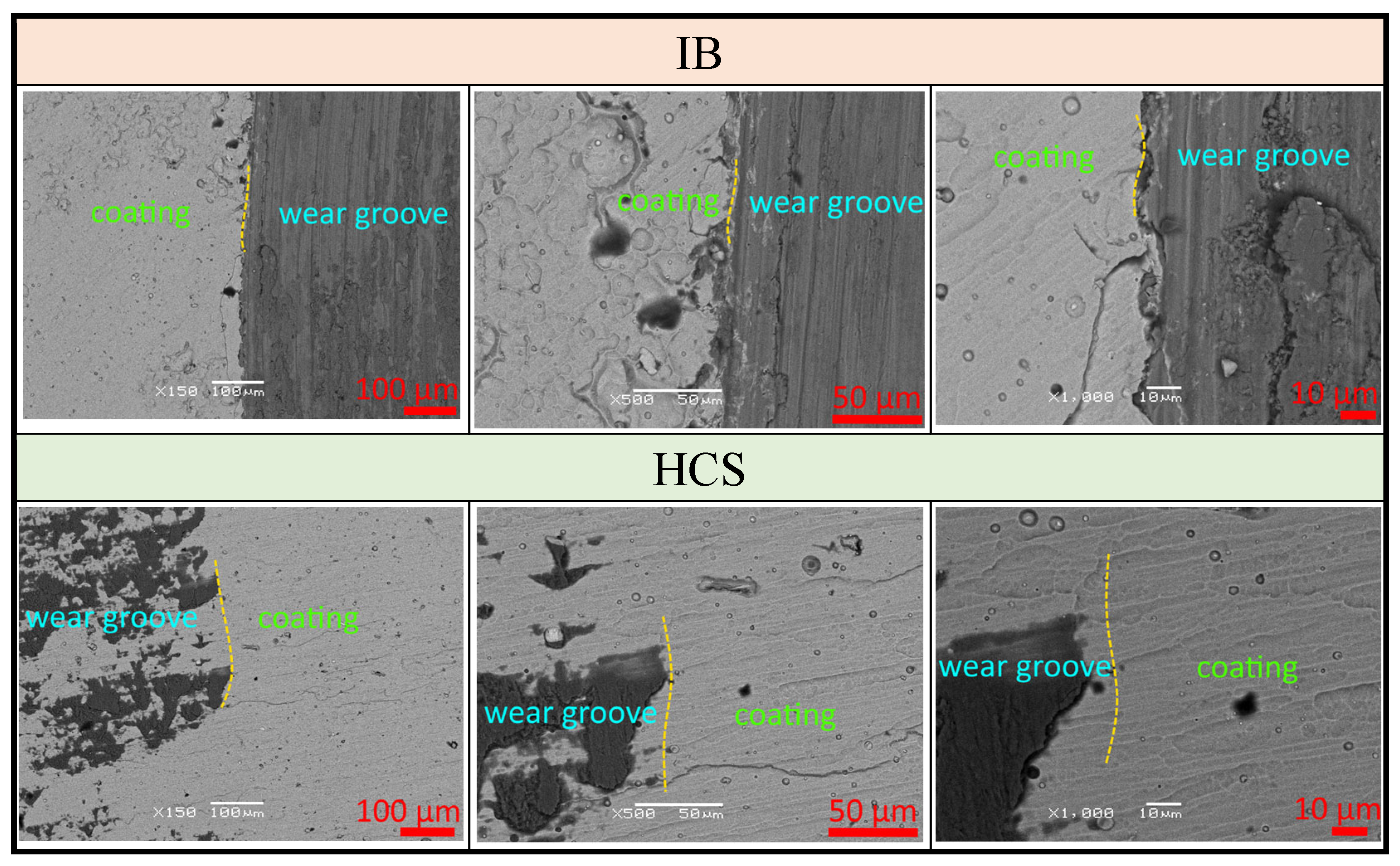
Figure 2 shows the surface appearance of IB and HCS samples at the wear groove boundary after the pin-on-disk test. Sample IB exhibits a clearly defined wear groove boundary, with the coating completely lost within the groove. Sample HCS exhibits a less defined wear groove boundary, with only partial coating loss within the groove itself.

3.2. Determination of the Optimal Bias Voltage of the HCS Process Substrate

Since the substrate bias voltage plays a significant role in the HCS method, studies were conducted to determine the optimal value of this parameter: 10 µm.
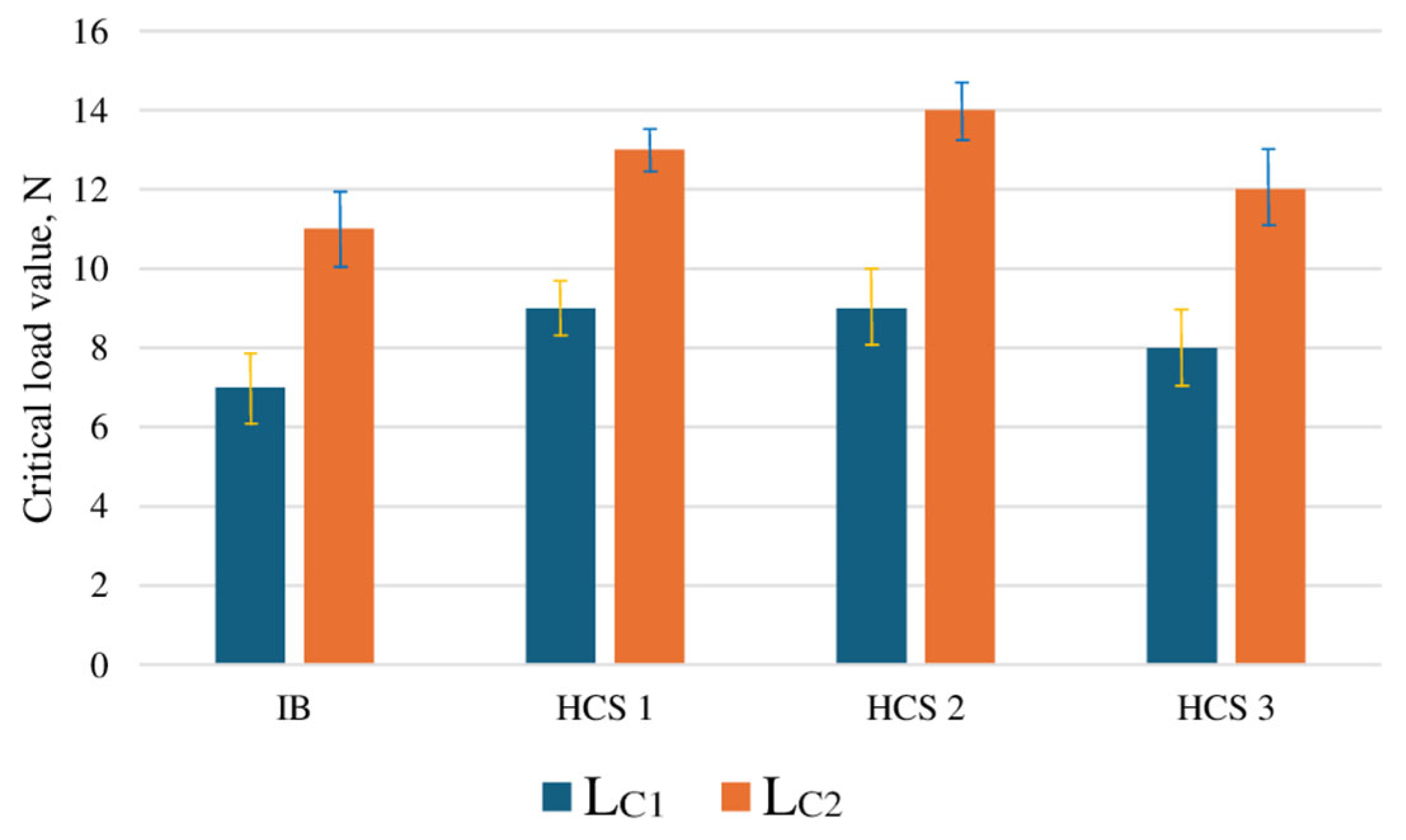
The results of the scratch test for the coated specimens are presented in Figure 3. The specimen with the HCS 2 coating (substrate bias voltage −1200 V) demonstrated the best fracture resistance (LC2 = 14 N). All three HCS specimens demonstrated better fracture resistance (LC2 = 11–15 N) compared to the IB specimen (LC2 = 10–12 N).
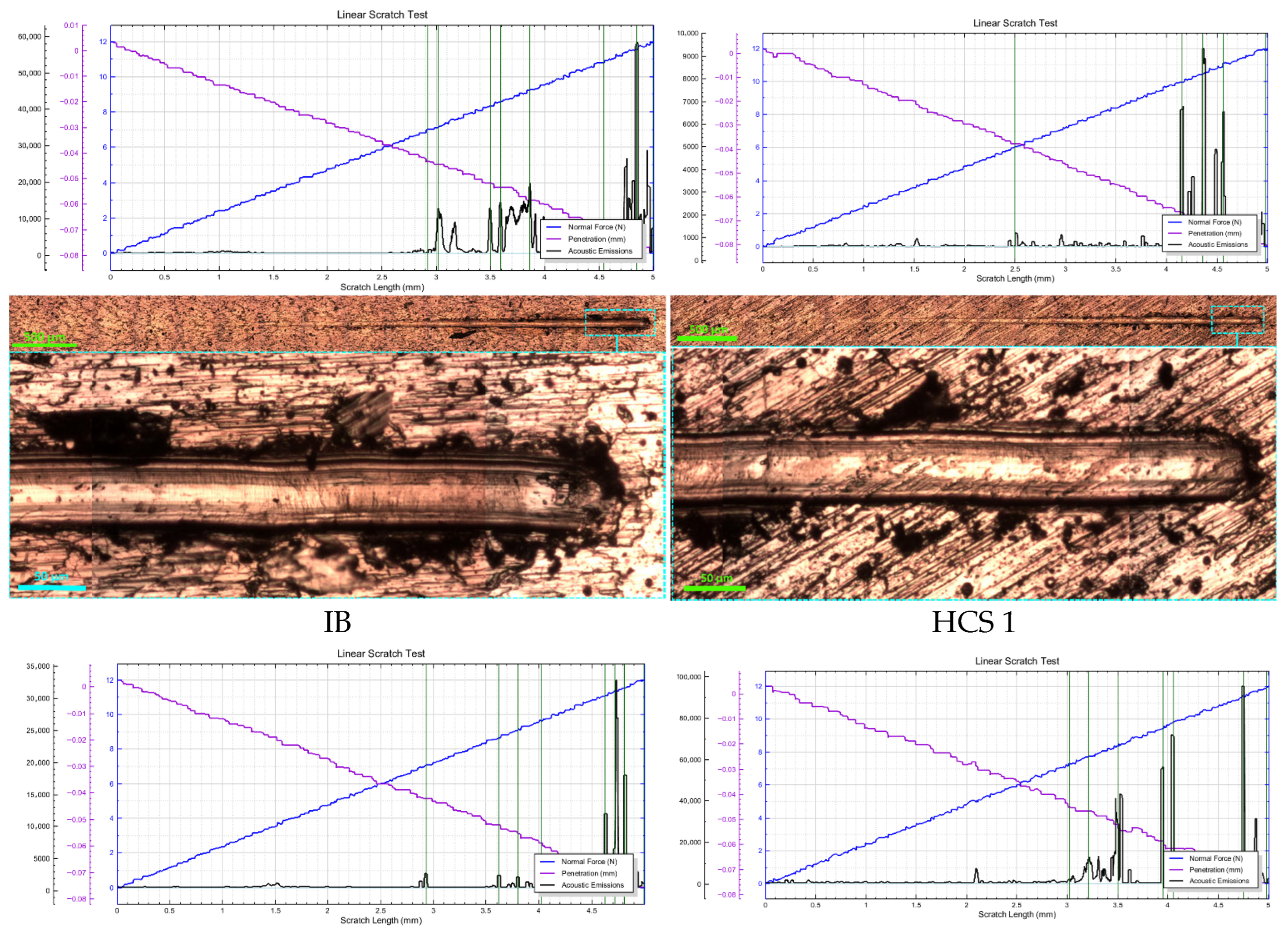
An examination of the scribing grooves and acoustic emission signal data (Figure 4) shows that the IB coating fails with noticeable delamination from the substrate. The delamination area reaches 50 µm from the wear groove boundaries. A similar failure pattern is also observed for samples with HCS 1 and HCS 3 coatings; however, delamination from the substrate in these cases occurs at a slightly higher load. The sample with the HCS 2 coating fails in a slightly different pattern. At critical loads, this sample exhibits localized delamination of the coating in an area no more than 20 µm from the wear groove boundaries. Upon reaching the maximum load of approximately 14 N, a spherical coating failure area forms. Presumably, at a given load, the indenter breaks through the coating, penetrating into a significantly softer substrate (as happens, for example, when measuring hardness, when an indenter at a certain load breaks through the coating and penetrates into the substrate).
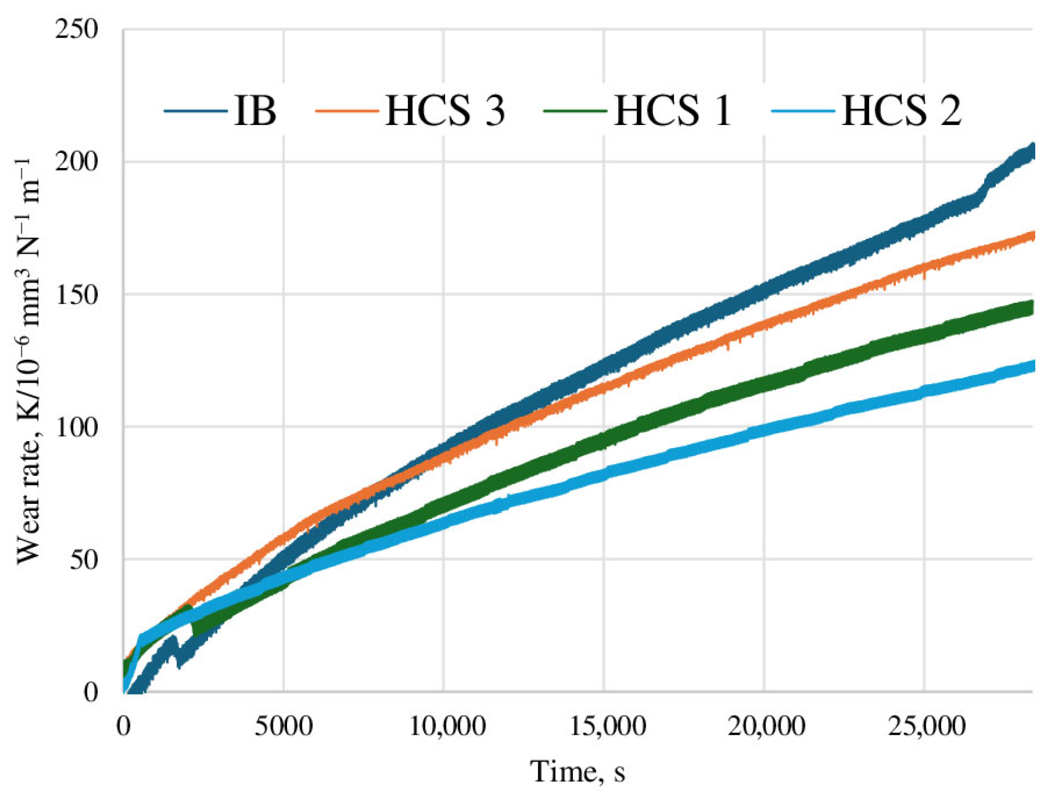
The results of the pin-on-disk wear resistance study for samples with different HCS process parameters are shown in Figure 5. Changing the bias voltage has a significant impact on wear resistance. In some cases, the wear resistance of the HCS samples is even lower than that of the IB sample. However, the best wear resistance is observed for the HCS 2 sample.
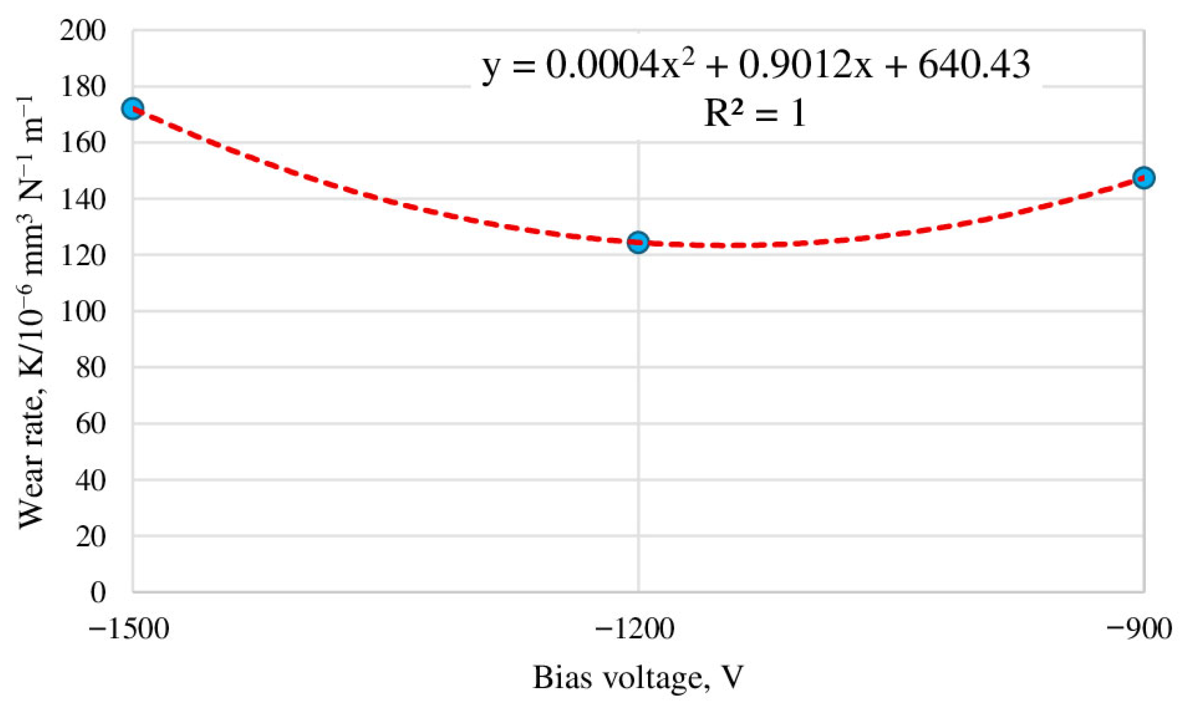
To find the optimal bias value, we plot graphs of wear rate versus bias voltage (Figure 6). We plot the wear values for each sample at the end of the experiment and then determine the type of dependence that best approximates the obtained data. As is well known, an approximating dependence (empirical formula) is an approximate functional dependence obtained from experimental data. We will solve the approximation problem, which consists of constructing a function that best smooths the experimental dependence and most accurately reflects the overall trend. To do this, we consider the approximation reliability (determination coefficient) R2, a statistical indicator that measures the proportion of variance in the dependent variable explained by the independent variables. For all three substrates, a second-degree polynomial dependence (quadratic function) most accurately reflects the overall trend (with the best value of R2 = 1). The corresponding dependencies are presented in the graphs (Figure 6).
Having obtained the approximating function, we determine the optimal value of the bias voltage. To do this, we determine the extremum point of the function. In our case, this is the point in the function’s domain where the function value reaches its minimum (the wear rate is minimal). Finding the extremum of a function involves finding the derivative of the function, determining the point at which the derivative is zero (or nonexistent if the function has a discontinuity), and checking whether the derivative changes sign at this point. A change in the derivative’s sign indicates the presence of a minimum.
We determine the optimal value of the bias voltage. The approximating relationship is defined by a quadratic formula
y = 0.0004   ·   x 2 + 0.9012   ·   x + 640.43 .
We find the first derivative of the function:
y   =   0.0008   ·   x   +   0.9012
We equate it to zero:
0.0008   ·   x   +   0.9012   =   0 ,
thereby
x 1 = 1126.5
We calculate the values of the function:
f ( 1126.5 )   =   121.126
Thus, the bias voltage value of −1126.5 V will provide wear rate = 121.126 K/10−6 mm3 N−1 m−1, which is lower than the wear rate at a bias voltage of −1200 V (122.985 K/10−6 mm3 N−1 m−1).
Let us check. We will use the sufficient condition for an extremum of a function of one variable. We will find the second derivative:
y   =   0.0008 .
We calculate
f ( 1126.5 ) = 0.0008 > 0
Thus, the minimum value of the function is obtained, corresponding to the optimal value of the substrate bias voltage, which ensures the minimum amount of wear.

3.3. Wear Behavior of Samples After Pin-on-Disk Testing

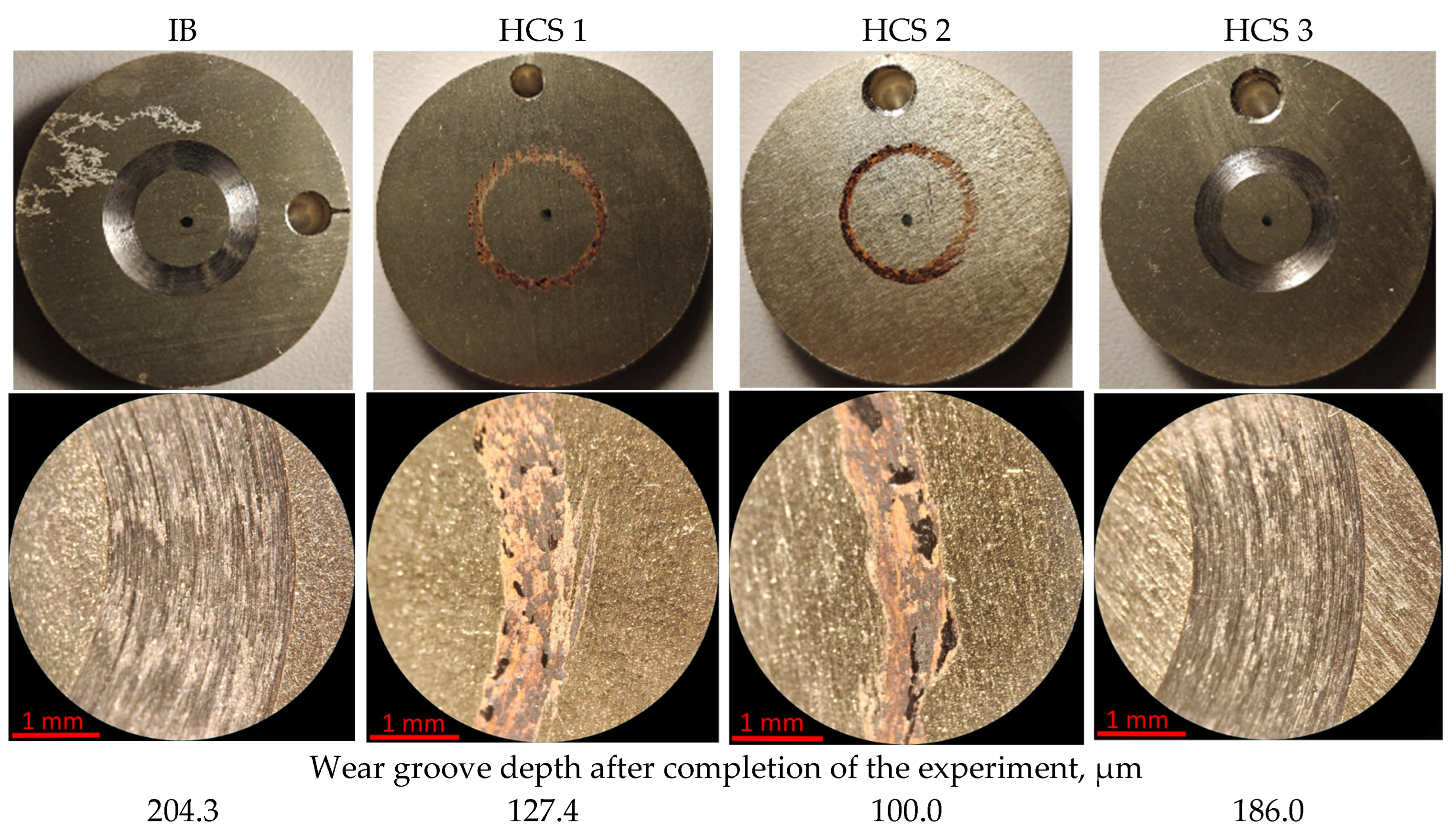
The wear pattern of the samples after the pin-on-disk test has certain differences (Figure 7). The highest wear intensity was observed for samples HCS 3 and IB. Samples HCS 1 and HCS 2 exhibited significantly lower wear intensity. Although the wear grooves on samples HCS 1 and HCS 2 appear virtually identical, previously obtained data (see Figure 4) indicate that sample HCS 2 exhibits slightly lower wear intensity. The wear groove on samples HCS 1 and HCS 2 lacks clear boundaries, and the coating within the groove remains largely intact. However, samples HCS 3 and IB exhibited distinct grooves with clearly visible boundaries. The wear groove depth of the HCS 3 and IB samples is also noticeably greater compared to the HCS 1 and HCS 2 samples.
To compare the wear pattern and the internal structure of the surface layer of the coated samples, HCS 2 samples, which showed the best wear resistance, and IB samples were selected.
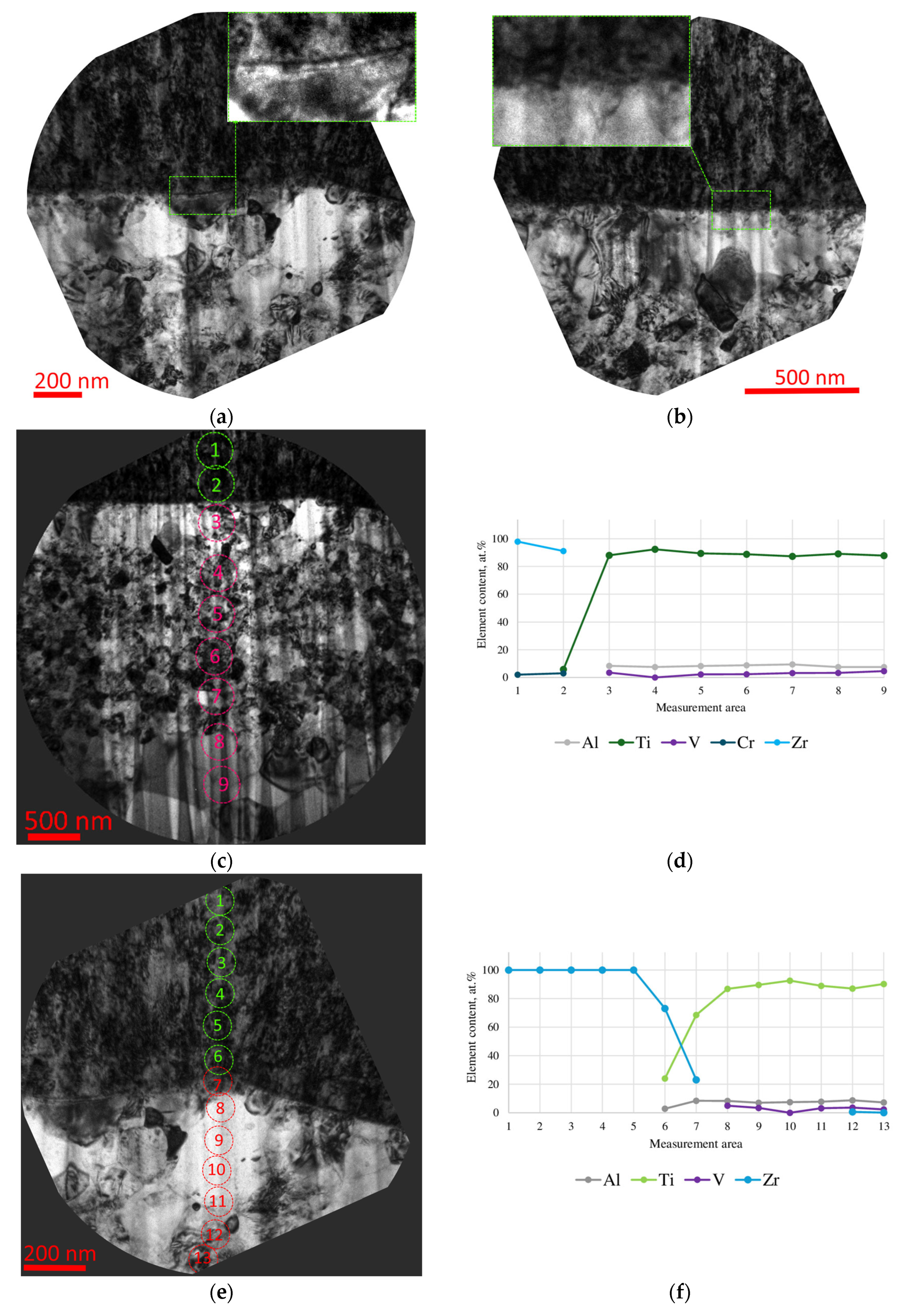
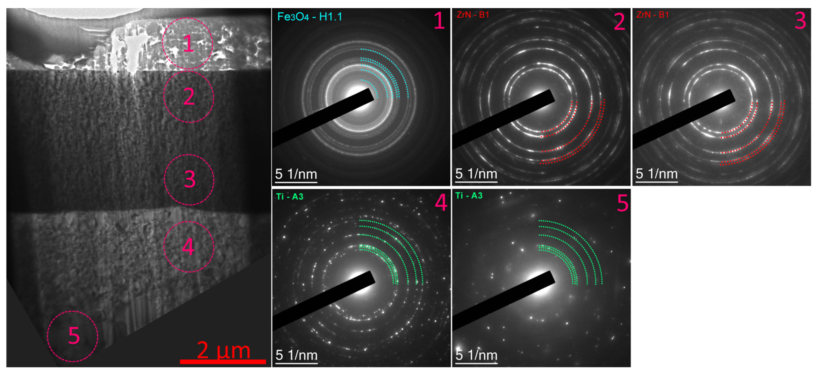
An analysis of the interface of the coating deposited using the HCS method on a 6Al-4V titanium alloy substrate shows that in some areas, a thin intermediate layer of approximately 20 nm thick is formed (Figure 8a), while in other areas, this layer is not clearly visible (Figure 8b). At the same time, the interface region contains a region of mixing of the coating (zirconium) and substrate (titanium and aluminum) materials (zones 6 and 7, Figure 8e and zone 3 in Figure 8g). On average, this region contains approximately equivalent titanium and zirconium contents (46–47 at.%) with an insignificant presence of aluminum and vanadium (3–5 at.%). Thus, based on the analysis of the elemental content, it can be concluded that there is a transition layer of approximately 100 nm thickness.
There is slight adhesion of titanium into the coating to a depth of 200 nm (Figure 8a,b), while no noticeable adhesion of zirconium to the substrate is observed. A deposit of oxidized indenter material (steel) is present on the sample surface (Figure 8c,d). Analysis of the elemental composition of the interface layer reveals a fairly distinct boundary between the coating and substrate (Figure 8k–n). Significant diffusion of titanium from the substrate into the coating and significantly less diffusion of zirconium from the coating into the substrate occur.
Surface element deposition analysis (SAED) of the substrate and coating reveals an Fe3O4 (H1.1) iron oxide phase in the oxidized deposit of the indenter material, while the coating is represented by a single ZrN (B1) phase, and a Ti (A3) phase is observed in the substrate (Figure 9).
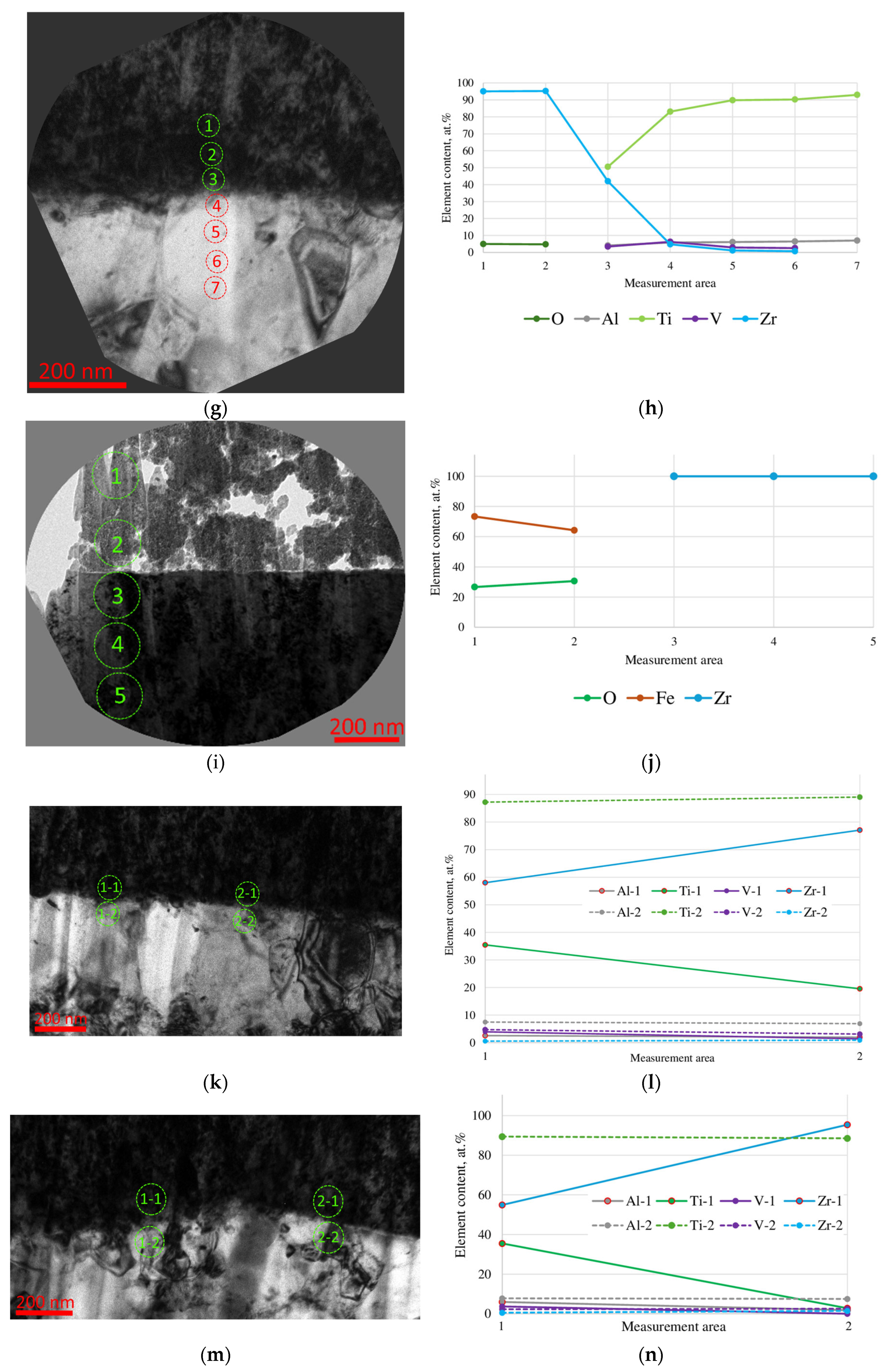
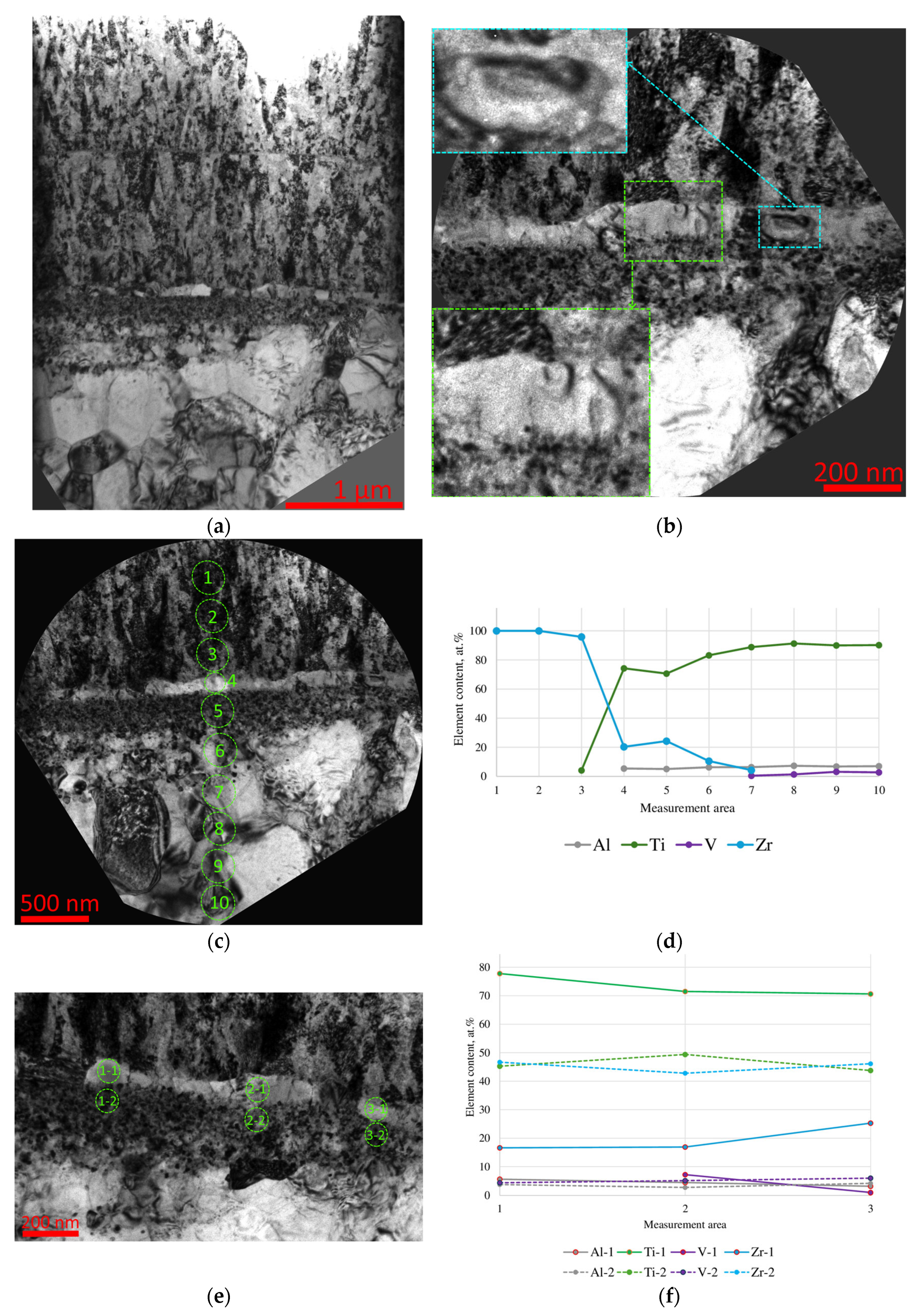
An examination of the internal structure and composition of the interface between the substrate and the ZrN coating deposited using the IB technology reveals the presence of a transition layer approximately 100 nm thick (Figure 10a,b). In terms of elemental composition, this layer is formed by a mixture of titanium (approximately 75 at.%), zirconium (approximately 20 at.%), and aluminum (approximately 5 at.%) (Figure 10c,d). Significant diffusion of zirconium into the substrate (to a depth of up to 1 μm) is observed, as is titanium diffusion from the substrate into the coating to a depth of up to 250 nm. Vanadium is completely absent or present in extremely small quantities in the surface layers of the substrate (approximately 600 nm from the boundary with the coating). Along the interface layer, a mixing region is observed, formed primarily by zirconium (from the coating composition) and titanium (from the substrate) (Figure 10e,f). Of particular interest is the light-contrast sublayer dominated by titanium (regions 1-1, 2-1, and 3-1), while the dark-contrast sublayer located closer to the substrate is formed by a nearly equal content of titanium and zirconium (regions 1-2, 2-2, and 3-2). This anomalous diffusion behavior of titanium is of particular interest and requires further study.
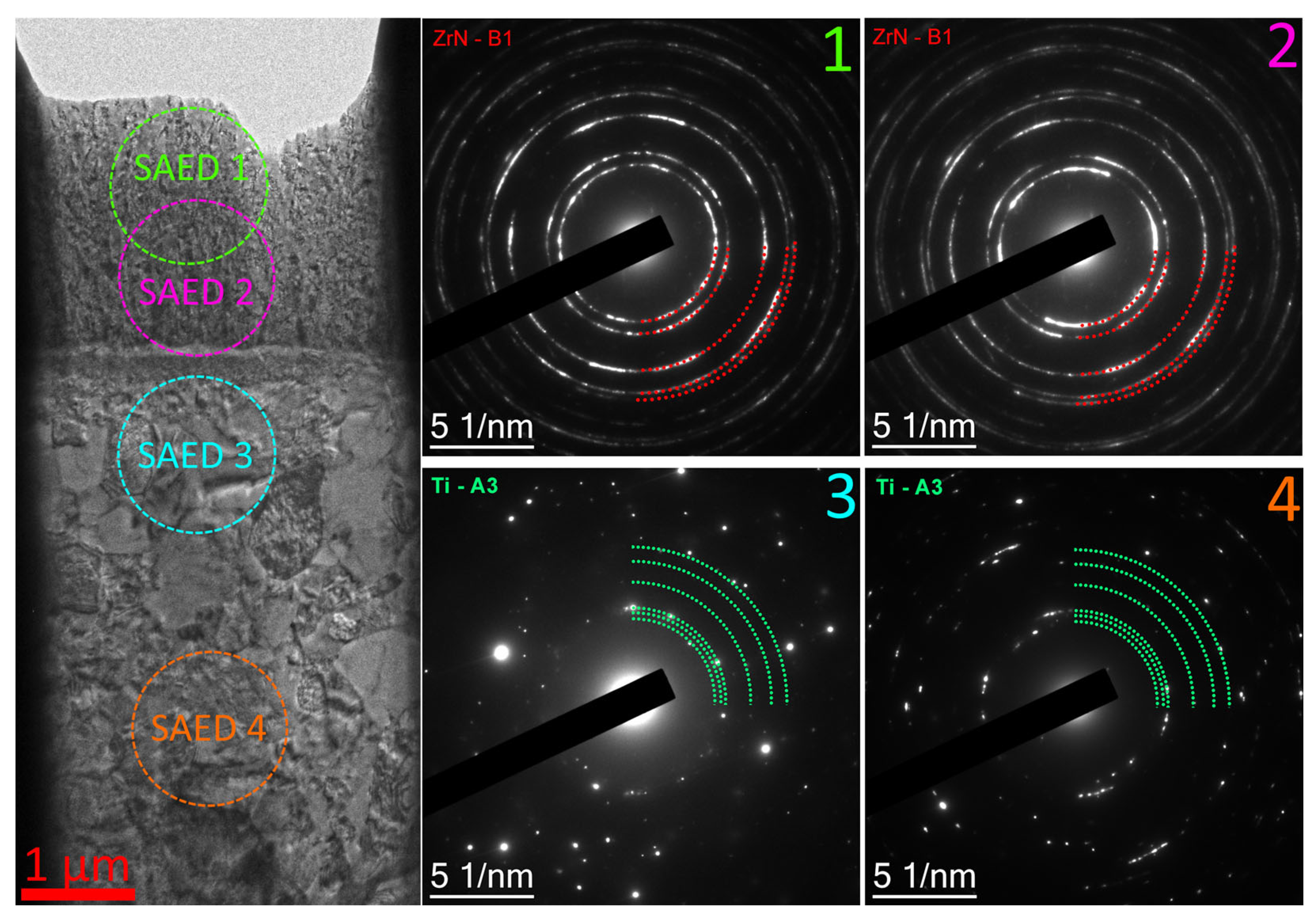
Studies of the phase composition of the surface layers of the substrate and coating (SAED) show that the coating is represented by a single phase of ZrN (B1), while in the substrate, only the Ti (A3) phase is observed (Figure 11).

4. Conclusions

  • After deposition of the coatings, the wear resistance of the samples increases by 50–70% compared to samples made of uncoated 6Al-4V titanium alloy, while the use of the HCS method provides wear resistance that is 30% higher than the IB method.
  • Studies of the friction coefficient show that the deposition of coatings provides a reduction in this parameter from 0.5 to 0.3 (by 65%). At the same time, samples with coatings deposited using the HCS and IB methods demonstrate very close values of the friction coefficient, with an insignificant (10–15%) reduction in this indicator for HCS samples.
  • The use of Ion Bombardment (IB) or glow discharge (HCS) methods significantly affects the wear resistance of the coating, but only slightly affects the coefficient of friction.
  • Changing the bias voltage on the substrate (−900, −1200, and −1500 V) has a significant effect on wear resistance. The best wear resistance is observed for the HCS sample with a bias voltage of −1200 V. The calculated optimum value of the bias voltage is −1126 V.
  • During the pre-treatment of the substrate using the HCS and IB methods, a transition layer can be formed in the area of the coating–substrate interface; the thickness of this layer varies within the range of 15–400 nm, and the composition is a mixture of coating (zirconium) and substrate (titanium, aluminum, and vanadium) materials.
  • When using the HCS method, a clearly defined interface is formed between the coating and the substrate, with preferential diffusion of titanium from the substrate into the adjacent layers of the coating; when using the IB method, the interface has a complex layered shape with noticeable mutual diffusion of titanium and zirconium.

Author Contributions

Conceptualization, A.V., Y.B. and C.S.; Methodology, A.M., Y.B., C.S., Y.M., F.M. and A.S.; Resources, A.M.; Data Curation, A.M., C.S., T.B. and Y.P.; Investigation, C.S., F.M., A.S., I.S., T.B., Y.M. and Y.P.; Supervision, A.M. and Y.B.; Writing—Original Draft Preparation, A.V.; Writing—Review and Editing, A.V., T.B. and C.S.; Project Administration, A.M., Y.M. and C.S. All authors have read and agreed to the published version of the manuscript.

Funding

This work was funded by the Russian Science Foundation (grant no. 23-19-00517).

Institutional Review Board Statement

Not applicable.

Informed Consent Statement

Not applicable.

Data Availability Statement

The original contributions presented in the study are included in the article; further inquiries can be directed to the corresponding author.

Conflicts of Interest

Author Yuri Potapov is employed by the Joint-Stock Company. The remaining authors declare that the research was conducted in the absence of any commercial or financial relationships that could be construed as a potential conflict of interest.

References

  1. Frey, H.; Khan, H.R. Handbook of Thin Film Technology; Springer: Berlin/Heidelberg, Germany, 2015. [Google Scholar]
  2. Ilyin, A.A.; Plihunov, V.V.; Petrov, L.M.; Zelenkov, V.V.; Ivanchuk, S.B.; Sokolov, I.V. Cleaning and Activation of the Surface of Products from Structural Metallic Materials in the Process of Vacuum Ion-Plasma Treatment. Technol. Light Alloy. 2009, 2, 111–117. [Google Scholar]
  3. Luchkin, A.G.; Luchkin, G.S. Cleaning the Surface of Substrates for Coating by Vacuum-Plasma Methods. Bull. Kazan Technol. Univ. 2012, 15, 208–210. [Google Scholar]
  4. Oura, K.; Lifshitz, V.G.; Saranin, A.A.; Zotov, A.V.; Katayama, M. Introduction to Surface Physics; Nauka: Moscow, Russia, 2006. [Google Scholar]
  5. Tillmann, W.; Hagen, L.; Stangier, D.; Krabiell, M.; Elbers, M. Influence of etching-pretreatment on nano-grained WC-Co surfaces and properties of PVD/HVOF duplex coatings. Surf. Coat. Technol. 2019, 374, 32–43. [Google Scholar] [CrossRef]
  6. Pemmasani, S.P.; Valleti, K.; Gundakaram, R.C.; Rajulapati, K.V.; Mantripragada, R.; Koppoju, S.; Joshi, S.V. Effect of microstructure and phase constitution on mechanical properties of Ti1−xAlxN coatings. Appl. Surf. Sci. 2014, 313, 936–946. [Google Scholar] [CrossRef]
  7. Yang, J.; Odén, M.; Johansson-Jõesaar, M.P.; Esteve, J.; Llanes, L. Mechanical strength of ground WC-Co cemented carbides after coating deposition. Mater. Sci. Eng. A 2017, 689, 72–77. [Google Scholar] [CrossRef]
  8. Barshilia, H.C.; Ananth, A.; Khan, J.; Srinivas, G. Ar + H2 plasma etching for improved adhesion of PVD coatings on steel substrates. Vacuum 2012, 86, 1165–1173. [Google Scholar] [CrossRef]
  9. Buchwalder, A.; Zenker, R. Pre- and post-surface treatments using electron beam technology for load-related application of thermochemical and PVD hard coatings on soft substrate materials. Surf. Coat. Technol. 2019, 375, 920–932. [Google Scholar] [CrossRef]
  10. Guo, X.; Liu, F.; Zhang, K.; Wang, C.; Piao, Z.; Sun, L. Controllable preparation of micro-textures on WC/Co substrate surface by an integrated laser-dry etching process for improving PVD coatings adhesion. Appl. Surf. Sci. 2020, 534, 147580. [Google Scholar] [CrossRef]
  11. Zhang, K.D.; Deng, J.X.; Guo, X.H.; Sun, L.N.; Lei, S.T. Study on the adhesion and tribological behavior of PVD TiAlN coatings with a multi-scale textured substrate surface. Int. J. Refract. Met. Hard Mater. 2018, 72, 292–305. [Google Scholar] [CrossRef]
  12. Meng, X.; Zhang, K.; Guo, X.; Wang, C.; Sun, L. Preparation of micro-textures on cemented carbide substrate surface by plasma-assisted laser machining to enhance the PVD tool coatings adhesion. J. Mater. Process. Technol. 2021, 288, 116870. [Google Scholar] [CrossRef]
  13. Stepanovsky, A.S. Ionic Processing of Materials. Mech. Eng. Sci. Technol. 2013, 14, 1–3. [Google Scholar]
  14. Komarovskaya, V.M.; Ivashchenko, S.A. Optimization of modes of ion treatment of the surface of non-metallic materials. Hardening Technol. Coat. 2013, 3, 23–27. [Google Scholar]
  15. Zabrodin, I.G.; Zorina, M.V.; Kaskov, I.A.; Malyshev, I.V.; Mikhailenko, M.S.; Pestov, A.E.; Salashchenko, N.N.; Chernyshev, A.K.; Chkhalo, N.I. Ion-beam techniques for precision processing of optical surfaces. J. Tech. Phys. 2020, 90, 1922–1930. [Google Scholar]
  16. Grebenyuk, V.F.; Rudakov, V.I. Ion-plasma technology for hardening a deforming tool. Vestn. OGU 2003, 5, 137–140. [Google Scholar]
  17. Berlin, E.; Dvinin, S.; Seidman, L. World of Materials and Technologies. In Vacuum Technology and Equipment for Deposition and Etching of Thin Films; Technosphere: Moscow, Russia, 2007. [Google Scholar]
  18. Hovsepian, P.; Reinhard, C.; Ehiasarian, A.P. CrAlYN/CrN superlattice coatings deposited by the combined high power impulse magnetron sputtering/unbalanced magnetron sputtering technique. Surf. Coat. Technol. 2006, 201, 4105–4110. [Google Scholar] [CrossRef]
  19. Berish, R. Problems of Applied Physics. In Sputtering of Solids by Ion Bombardment; Springer: Berlin/Heidelberg, Germany, 1986; Volume II, p. 482. [Google Scholar]
  20. Lieberman, M.A.; Lichtenberg, A.J. Principles of Plasma Discharges and Materials Processing; John Wiley & Sons: Hoboken, NJ, USA, 2005. [Google Scholar]
  21. Lattemann, M.; Ehiasarian, A.P.; Bohlmark, J.; Persson, P.; Helmersson, U. Investigation of high power impulse magnetron sputtering pretreated interfaces for adhesion enhancement of hard coatings on steel. Surf. Coat. Technol. 2006, 200, 6495–6499. [Google Scholar] [CrossRef]
  22. Mukha, I.M.; Shcherbakova, L.I. Effect of Heating by a Glow Discharge on the Surface State of Transition-Metal Carbides. Elektron. Obrab. Mater. 1976, 3, 53–56. [Google Scholar]
  23. Betiuk, M.; Michalski, J.; Burdyński, K.; Wach, P.; Nakonieczny, A. Influence of ion etching in low pressure arc discharge in plasma on duplex coat adhesion produced by gas nitriding and PA-PVD-Arc processes. Mater. Manuf. Process. 2009, 24, 859–862. [Google Scholar] [CrossRef]
  24. Breidenstein, B.; Denkena, B. Significance of residual stress in PVD-coated carbide cutting tools. CIRP Ann. Manuf. Technol. 2013, 62, 67–70. [Google Scholar] [CrossRef]
  25. Denkena, B.; Breidenstein, B. Residual stress gradients in PVD-coated carbide cutting tools. Mater. Sci. Forum 2006, 524–525, 607–612. [Google Scholar]
  26. Gassner, M.; Schalk, N.; Sartory, B.; Pohler, M.; Czettl, C.; Mitterer, C. Influence of Ar ion etching on the surface topography of cemented carbide cutting inserts. Int. J. Refract. Met. Hard. Mater. 2017, 69, 234–239. [Google Scholar] [CrossRef]
  27. Yang, J.; Odén, M.; Johansson-Jõesaar, M.P.; Llanes, L. Grinding effects on surface integrity and mechanical strength of WC-Co cemented carbides. Procedia CIRP 2014, 13, 257–263. [Google Scholar] [CrossRef]
  28. Grigoriev, S.; Vereschaka, A.; Zelenkov, V.; Sitnikov, N.; Bublikov, J.; Milovich, F.; Andreev, N.; Sotova, C. Investigation of the influence of the features of the deposition process on the structural features of microparticles in PVD coatings. Vacuum 2022, 202, 111144. [Google Scholar] [CrossRef]
  29. Kablov, E.N.; Muboyadzhyan, S.A. Ion etching and surface modification of critical machine parts in vacuum-arc plasma. Bull. MSTU Im. N.E. Bauman 2011, 2, 149–162. [Google Scholar]
  30. Mattox, M.D. Handbook of Physical Vapor Deposition (PVD) Processing, 2nd ed.; William Andrew: Norwich, NY, USA, 2010. [Google Scholar]
  31. Broitman, E.; Hultman, L. Adhesion improvement of carbon-based coatings through a high ionization deposition technique. J. Phys. Conf. Ser. 2012, 370, 012009. [Google Scholar] [CrossRef]
  32. Panjan, M. Influence of substrate rotation and target arrangement on the periodicity and uniformity of layered coatings. Surf. Coat. Technol. 2013, 235, 32–44. [Google Scholar] [CrossRef]
  33. Panjan, P.; Drnovšek, A.; Gselman, P.; Čekada, M.; Panjan, M. Review of Growth Defects in Thin Films Prepared by PVD Techniques. Coatings 2020, 10, 447. [Google Scholar] [CrossRef]
  34. Panjan, P.; Drnovšek, A.; Mahne, N.; Čekada, M.; Panjan, M. Surface Topography of PVD Hard Coatings. Coatings 2021, 11, 1387. [Google Scholar] [CrossRef]
  35. Schönjahn, C.; Lewis, D.B.; Münz, W.-D.; Petrov, I. Shortlisted substrate ion etching in combined steered cathodic arc–ubm deposition system: Effects on interface architecture, adhesion, and tool performance. Surf. Eng. 2000, 16, 176–180. [Google Scholar] [CrossRef]
  36. Panjan, P.; Drnovšek, A.; Čekada, M.; Panjan, M. Contamination of Substrate-Coating Interface Caused by Ion Etching. Coatings 2022, 12, 846. [Google Scholar] [CrossRef]
  37. Zadorozhnyi, V.G.; Rafalovich, D.M.; Roikh, I.L. Effect of Surface Treatment of Steel with a Glow Discharge on the Adhesion and Porosity of Vacuum Coatings of Polyfluorotrichloroethylene. Elektron. Obrab. Mater. 1977, 1, 43–45. [Google Scholar]
  38. Vetter, J.; Burgmer, W.; Perry, A.J. Arc-enhanced glow discharge in vacuum arc machines. Surf. Coat. Technol. 1993, 59, 152–155. [Google Scholar] [CrossRef]
  39. Wang, Y.H.; Guo, F.; Ren, H.; Hu, S.Y.; Chen, Y.J.; Zhao, Y.H.; Gong, F.; Xie, Z.W. Enhancing wear resistance of TiN coating by gradient bias voltage and arc-enhanced glow discharge. Ceram. Int. 2022, 48, 8746–8750. [Google Scholar] [CrossRef]
  40. Xue, G.; Wang, Z.; Xiang, L.; Xiao, H.; Zhao, Y.; Wan, Y.; Ning, H.; Xie, Z. Enhancing hot corrosion performance of NiCoCrAlY/AlSiY coating by arc enhanced glow discharge. Mater. Lett. X 2022, 13, 100130. [Google Scholar] [CrossRef]
  41. Marciniak, A. Non-uniform heating effects during treatment in a glow discharge. Thin Solid Film. 1988, 156, 337–344. [Google Scholar] [CrossRef]
  42. Samir, T.; Liu, Y.; Zhao, L.-L.; Zhou, Y.-W. Effect of driving frequency on electron heating in capacitively coupled RF argon glow discharges at low pressure. Chin. Phys. B 2017, 26, 115201. [Google Scholar] [CrossRef]
  43. Grigoriev, S.; Melnik, Y.; Metel, A. Broad fast neutral molecule beam sources for industrial-scale beam-assisted deposition. Surf. Coat. Technol. 2002, 156, 44–49. [Google Scholar] [CrossRef]
  44. Bublikov, J.; Volosova, M.; Vereschaka, A.; Milovich, F.; Seleznev, A.; Shmakov, I.; Grigoriev, S. Hollow cathode effect in a glow discharge for cleaning and heating substrate surfaces during wear-resistant coating deposition. J. Mater. Res. Technol. 2025, 39, 7657–7670. [Google Scholar] [CrossRef]
  45. Wei, G.; Tan, M.; Attarilar, S.; Uglov, V.V.; Wang, B.; Liu, J.; Lu, L.; Wang, L. An overview of surface modification, A way toward fabrication of nascent biomedical Ti–6Al–4V alloys. J. Mater. Res. Technol. 2023, 24, 5896–5921. [Google Scholar] [CrossRef]
  46. Freitas, B.J.M.; Vidilli, A.L.; de Bribean Guerra, A.; Ferreira, D.C.F.; Kasama, A.H.; Paes, M.T.P.; Koga, G.Y.; Bolfarini, C. Ti-6Al-4V and Ti-6Al-4V-0.1Ru alloys in oil and gas exploration: A review of performance and hydrogen embrittlement. J. Alloys Compd. 2025, 1019, 179258. [Google Scholar] [CrossRef]
  47. Liu, W.; Liu, Z. High-pressure coolant effect on the surface integrity of machining titanium alloy Ti-6Al-4V: A review. Mater. Res. Express 2018, 5, 032001. [Google Scholar] [CrossRef]
  48. ASTM F1472-20a; Standard Specification for Wrought Titanium-6Aluminum-4Vanadium Alloy for Surgical Implant Applications (UNS R56400). ASTM International: West Conshohocken, PA, USA, 2023. [CrossRef]
  49. Arias, D.F.; Arango, Y.C.; Devia, A. Study of TiN and ZrN thin films grown by cathodic arc technique. Appl. Surf. Sci. 2006, 253, 1683–1690. [Google Scholar] [CrossRef]
  50. Harrison, R.W.; Lee, W.E. Processing and properties of ZrC, ZrN and ZrCN ceramics: A review. Adv. Appl. Ceram. 2016, 115, 294–307. [Google Scholar] [CrossRef]
  51. Patsalas, P. Zirconium nitride: A viable candidate for photonics and plasmonics? Thin Solid Film. 2019, 688, 137438. [Google Scholar] [CrossRef]
  52. Aristova, N.M.; Onufriev, S.V.; Savvatimskiy, A.I. Thermodynamic properties of zirconium nitride in the condensed state. Phys. Uspekhi 2024, 67, 1022–1033. [Google Scholar] [CrossRef]
  53. Slaymaker, J.; Rossouw, E.; Michelogiannakis, D. The influence of protective coatings on corrosion resistance in orthodontic magnets: A systematic review of in vitro studies. Int. Orthod. 2026, 24, 101080. [Google Scholar] [CrossRef]
  54. Grigoriev, S.; Vereschaka, A.; Milovich, F.; Sitnikov, N.; Andreev, N.; Bublikov, J.; Kutina, N. Investigation of the properties of the Cr,Mo-(Cr,Mo,Zr,Nb)N-(Cr,Mo,Zr,Nb,Al)N multilayer composite multicomponent coating with nanostructured wear-resistant layer. Wear 2021, 468–469, 203597. [Google Scholar] [CrossRef]
  55. Vereschaka, A.A.; Bublikov, J.I.; Sitnikov, N.N.; Oganyan, G.V.; Sotova, C.S. Influence of nanolayer thickness on the perfor-mance properties of multilayer composite nano-structured modified coatings for metal-cutting tools. Int. J. Adv. Manuf. Technol. 2018, 95, 2625–2640. [Google Scholar] [CrossRef]
  56. Grigoriev, S.; Vereschaka, A.; Milovich, F.; Migranov, M.; Andreev, N.; Bublikov, J.; Sitnikov, N.; Oganyan, G. Investigation of the tribological properties of Ti-TiN-(Ti,Al,Nb,Zr)N composite coating and its efficiency in increasing wear resistance of metal cutting tools. Tribol. Int. 2021, 164, 107236. [Google Scholar] [CrossRef]
  57. Vereschaka, A.S.; Grigoriev, S.N.; Sotova, E.S.; Vereschaka, A.A. Improving the efficiency of the cutting tools made of mixed ceramics by applying modifying nano-scale multilayered coatings. Adv. Mater. Res. 2013, 712–715, 391–394. [Google Scholar]
  58. Metel, A.; Bolbukov, V.; Volosova, M.; Grigoriev, S.; Melnik, Y. Equipment for Deposition of thin metallic films bombarded by fast argon atoms. Instrum. Exp. Tech. 2014, 57, 345–351. [Google Scholar] [CrossRef]
  59. Metel, A.S.; Grigoriev, S.N.; Melnik, Y.A.; Bolbukov, V.P. Characteristics of a fast neutral atom source with electrons injected into the source through its emissive grid from the vacuum chamber. Instrum. Exp. Tech. 2012, 55, 288–293. [Google Scholar] [CrossRef]
  60. Grigoriev, S.; Vereschaka, A.; Milovich, F.; Sitnikov, N.; Seleznev, A.; Sotova, C.; Bublikov, J. Influence of the yttrium cathode arc current on the yttrium content in the (Ti,Y,Al) N coating and the coating properties. Vacuum 2024, 222, 113028. [Google Scholar] [CrossRef]
  61. ASTM C1624-05; Standard Test Method for Adhesion Strength and Mechanical Failure Modes of Ceramic Coatings by Quantitative Single Point Scratch Testing. ASTM International: West Conshohocken, PA, USA, 2010. [CrossRef]
  62. ASTM G99-23; Standard Test Method for Wear and Friction Testing with a Pin-on-Disk or Ball-on-Disk Apparatus. ASTM: West Conshohocken, PA, USA, 2023. Available online: https://store.astm.org/standards/g99 (accessed on 22 June 2025).
  63. Sotova, C.; Bublikov, Y.; Seleznev, A.; Shmakov, I.; Vereschaka, A. Study of the effect of healing surface defects during deposition of nitride coatings on titanium alloy parts. High Temp. Mater. Process. 2025, 29, 1–8. [Google Scholar] [CrossRef]
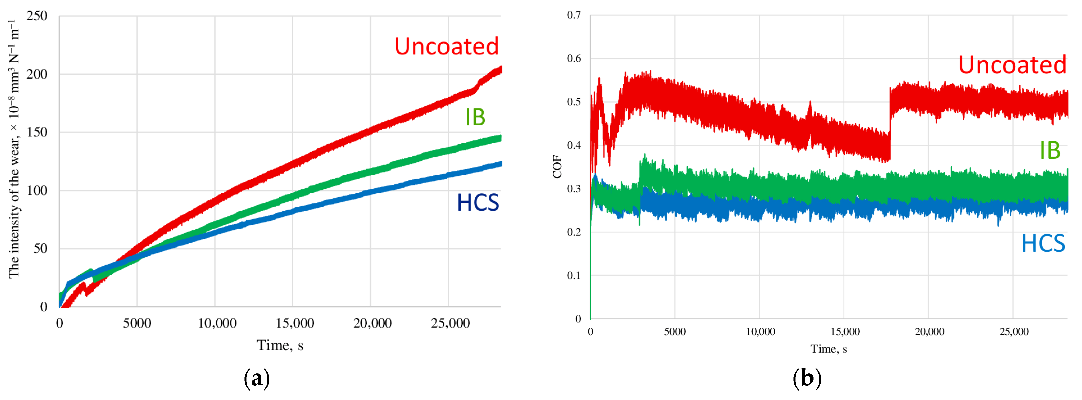
Figure 1. Results of the study of wear resistance (a) and the coefficient of friction (b) of coated samples and the reference sample without coating in the pin-on-disk test.
Jcs 09 00640 g001
Figure 2. Nature of destruction of samples with IB and HCS coatings (SEM).
Jcs 09 00640 g002
Figure 3. Results of the study of the fracture resistance of samples with coatings using the scratch test. LC1 is the initial failure load, LC2 is the complete failure load.
Jcs 09 00640 g003
Figure 4. The nature of destruction of HCS and IB coatings on a 6Al-4V titanium alloy substrate during a scratch test. Acoustic emission signal (top), photo of scribing grooves and enlarged view of the groove end (optical microscope, bottom).
Jcs 09 00640 g004aJcs 09 00640 g004b
Figure 5. Degree of wear of samples depending on time during pin-on-disk test.
Jcs 09 00640 g005
Figure 6. Wear rate versus bias voltage. Finding the approximating function.
Jcs 09 00640 g006
Figure 7. General view of wear grooves and wear pattern of samples after pin-on-disk test (optical microscope), wear groove depth after completion of the experiment.
Jcs 09 00640 g007
Figure 8. Internal structure and composition of the surface layer of a 6Al-4V titanium alloy sample with HCS 2 coating in a pin-on-disk test: (a,b)—interface layer structure; (ch)—change in elemental composition along the line perpendicular to the interface layer; (i,j)—coating composition in the area of the steel deposit; (kn)—change in elemental composition along the interface layer (TEM). The circles marked with a green dotted line indicate the areas where the composition is measured.
Jcs 09 00640 g008aJcs 09 00640 g008b
Figure 9. Phase composition of the surface layers of the 6Al-4V titanium alloy substrate and the HCS 2 (SAED) coating (TEM).
Jcs 09 00640 g009
Figure 10. Internal structure and composition of the surface layer of a 6Al-4V titanium alloy sample with an IB coating in a pin-on-disk test: (a,b)—structure of the interface layer; (c,d)—change in elemental composition along the line perpendicular to the interface layer; (e,f)—change in elemental composition along the interface layer (TEM). The circles marked with a green dotted line indicate the areas where the composition is measured.
Jcs 09 00640 g010
Figure 11. Phase composition of the surface layers of the substrate and IB coating (electron diffraction pattern—SAED) (TEM). The circles marked with a green dotted line indicate the areas where the phase composition is measured.
Jcs 09 00640 g011
Table 1. Chemical composition of titanium alloy 6Al-4V [48].
TiAlVFeZrOCSiNHOther
Impurities
86.45–90.905.3–6.83.5–5.3max 0.6max 0.3max 0.2max 0.1max 0.1max 0.05max 0.0150.3
Table 2. Designation of samples depending on the magnitude of the bias voltage on the substrate.
Designation of SamplesHCS 1HCS 2HCS 3
Substrate bias voltage, V−900 V−1200 V−1500 V
Table 3. Surface roughness of samples before and after coating deposition.
Roughness, µmUncoatedIBHCS
Ra10.224.943.58
Rz7.325.984.33
Disclaimer/Publisher’s Note: The statements, opinions and data contained in all publications are solely those of the individual author(s) and contributor(s) and not of MDPI and/or the editor(s). MDPI and/or the editor(s) disclaim responsibility for any injury to people or property resulting from any ideas, methods, instructions or products referred to in the content.