Article

First-Principles Study of Electronic and Optical Properties of Tri-Layered van der Waals Heterostructures Based on Blue Phosphorus and Zinc Oxide

by
Michael M. Slepchenkov
1,
Dmitry A. Kolosov
1 and
Olga E. Glukhova
1,2,*
1
Institute of Physics, Saratov State University, Astrakhanskaya Street 83, 410012 Saratov, Russia
2
Laboratory of Biomedical Nanotechnology, I.M. Sechenov First Moscow State Medical University, Trubetskaya Street 8-2, 119991 Moscow, Russia
*
Author to whom correspondence should be addressed.
J. Compos. Sci. 2022, 6(6), 163; https://doi.org/10.3390/jcs6060163
Submission received: 9 May 2022 / Revised: 24 May 2022 / Accepted: 30 May 2022 / Published: 2 June 2022

Abstract

:
The creation of van der Waals heterostructures with tunable properties from various combinations of modern 2D materials is one of the promising tasks of nanoelectronics, focused on improving the parameters of electronic nanodevices. In this paper, using ab initio methods, we theoretically predict the existence of new three-layer van der Waals zinc oxide/blue phosphorus/zinc oxide (ZnO/BlueP/ZnO) heterostructure with AAA, ABA, ABC layer packing types. It is found that AAA-, ABA-, and ABC-stacked ZnO/BlueP/ZnO heterostructures are semiconductors with a gap of about 0.7 eV. The dynamic conductivity and absorption spectra are calculated in the wavelength range of 200–2000 nm. It is revealed that the BlueP monolayer makes the greatest contribution to the formation of the profiles the dynamic conductivity and absorption coefficient spectrums of the ZnO/BlueP/ZnO heterostructure. This is indicated by the fact that, for the ZnO/BlueP/ZnO heterostructure, conductivity anisotropy is observed at different directions of wave polarization, as for blue phosphorus. It has been established that the absorption maximum of the heterostructure falls in the middle ultraviolet range, and, starting from a wavelength of 700 nm, there is a complete absence of absorption. The type of layer packing has practically no effect on the regularities in the formation of the spectra of dynamic conductivity and the absorption coefficient, which is important from the point of view of their application in optoelectronics.

1. Introduction

The urgent problem of nanoelectronics is to improve parameters and performance of electronic components. Solving this problem requires a careful selection of materials to create modern electronic components based on them. Currently, preference is given to nanostructured materials, among which the generation of new 2D materials is of the greatest interest [1]. In comparison with traditional 3D photonic materials such as gallium arsenide, 2D materials offer several advantages. First, due to quantum confinement in the direction perpendicular to the base plane, 2D materials acquire new electronic and optical properties that are absent in 3D materials [2]. Second, the natural passivation of the surface of 2D materials makes it easy to integrate them with photonic structures such as waveguides and resonance cavities [3,4]. Using various 2D materials, it is possible to create vertical heterostructures without facing the traditional problem of lattice mismatch between the materials being combined. Third, despite the atomic thickness, many 2D materials interact intensely with light [5]. In addition, due to a wide range of electronic properties, including the presence of a band gap ranging from a few millielectron volts to several electron volts, depending on the type of atoms in the lattice, 2D materials can cover a wide range of the electromagnetic spectrum from ultraviolet, visible and near infrared (IR) ranges up to the middle and far infrared ranges, as well as in the terahertz and microwave ranges [6].
A new stage in the development of nanoelectronics is associated with vertical heterostructures, which also named as van der Waals heterostructures, since the layers in them are held only by the action of van der Waals forces [7,8,9]. Van der Waals structures based on hexagonal boron nitride, carbon (graphene), phosphorus (phosphorene), germanium (germanene), boron (borophene), silicon (silicene), and tin (stanene) have already been obtained [10]. The group of promising 2D materials for electronics and photonics is also formed by representatives of transition metal dichalcogenides, including titanium disulfide, molybdenum disulfide, and tungsten diselenide [11,12,13,14,15,16], and also by representatives of 2D III-V semiconductors [17]. The first results of studies of van der Waals heterostructures have shown that this field of study is promising for the development of nano- and optoelectronic devices. In particular, tunnel field-effect transistors [18], thermoelectric devices [19], light-emitting diodes [20], solar panels [21], and sensors [22] have already been developed on the basis of graphene/hexagonal boron nitride heterostructures. Experimental and theoretical studies have been carried out on the possibility of creating Schottky barriers based on graphene/MoS2 [23], graphene/boron nitride [24], graphene/silicene [25], graphene/InSe [26], MoTe2/MoS2 [27], graphene/phosphorene van der Waals heterostructures and heterostructures based on phosphorene and MoSe2 allotropes [28]. Layered structures of transition metal dichalcogenides have shown themselves to be a promising material for the creation of optoelectronic devices [29,30,31]. MoS2 and WS2 based photocells operating in the visible range and near infrared (IF) range of the electromagnetic spectrum have been created [32,33,34,35]. For the development of photodetectors of ultraviolet (UV) radiation, promising materials are representatives of metal oxides, in particular zinc oxide and titanium dioxide, as well as representatives of semiconductor nitrides of the third group, such as gallium, aluminum, indium nitride [36]. Among modern single-element 2D materials, borophene, which is currently being successfully synthesized, deserves special attention [37,38]. The unique combination of such properties as mechanical strength and flexibility, lightness, high electrical conductivity, and optical transparency make borophene one of the most perspective candidates for nano- and optoelectronics. The emergence of new 2D materials, in particular blue phosphorus [39], requires additional fundamental study of the prospects for their use to create vertical heterostructures with desired properties. In particular, the attention of researchers is attracted by the possibility of combining blue phosphorus and zinc oxide monolayers to form vertical van der Waals heterostructures. First-principles studies of the electronic and optical properties of bilayer ZnO/BlueP 2D heterostructures have been carried out [40,41,42,43]. Based on the results of DFT calculations, it was found that bilayer ZnO/BlueP heterostructures are indirect semiconductors and have optical absorption peaks in the visible and ultraviolet regions. At the same time, for the successful application of layered van der Waals heterostructures based on ZnO and BlueP monolayers in optoelectronics, it is necessary to consider the possibilities of controlling their properties. In this paper, ab initio methods are used to study the possibility of topological control of the electronic and optical properties of van der Waals heterostructures based on ZnO and BlueP monolayers by adding a third layer, namely, one more ZnO monolayer. When considering this three-layer topological configuration ZnO/BlueP/ZnO, we set the following tasks: (1) to increase the thermodynamic stability of van der Waals heterostructure; (2) to control the energy gap of the band structure; (3) control the position of the absorption peaks in the spectrum of the absorption coefficient.

2. Computational Details

All the calculations of van der Waals heterostructures were performed using the density functional theory (DFT) in the Siesta 4.1.5 package [44,45]. The Perdew-Burke-Ernzerhof (PBE) generalized gradient approximation (GGA) was used to describe exchange-correlation effects [46]. The action of van der Waals forces between layers of heterostructure was taken into account using the exchange-correlation functional by K. Berland and P. Hyldgaard [47]. The geometry of the structure was optimized using the split-valence double zeta (DZ2P) basis set to converge the interatomic forces to 0.025 eV/Å. The Monkhorst-Pack scheme [48] with 12 × 6 × 1 k-point mesh was used for Brillouin zone sampling. A vacuum layer larger than 20 Å was used to avoid the interaction between layers in neighboring supercells. The mesh cutoff was set to 300 Ry.
The frequency-dependent complex dielectric function was calculated using the first order time dependent perturbation theory [49] in SIESTA package. The absorption coefficient was calculated as follows:
α ( ω ) = ω c n ( ω ) ε 2 ( ω ) ,
where n(ω) is the refractive index, ε2(ω) is the imaginary part of the complex dielectric function, c is the speed of light. The imaginary part ε2(ω) was determined by a summation of possible interband transitions from occupied to unoccupied states using the equation:
ε 2 ( ω ) = e 2 π m 2 ω 2 ν , c B Z d k | ψ c k | e ^ , p | ψ ν k | 2 δ ( E c ( k ) E ν ( k ) ω ) ,
where E(c,ν)(k) and ψ(c,ν),k are the energy and eigenfunction of unoccupied states in the conduction band (subscript c) and occupied states in the valence band (subscript ν), p is the momentum operator, ω is the photon energy, e ^ is the polarization vector, m is the electron mass. The optical characteristics were calculated for the energy range from 0.6 eV to 20 eV using optical broadening of 0.05 eV. Two different directions of light polarization were considered: vector E is parallel to the X axis; vector E is perpendicular to the X axis. The sampling of the Brillouin zone with a 114 × 65 × 1 k-points mesh was carried out when calculating the optical characteristics.

3. Results and Discussion

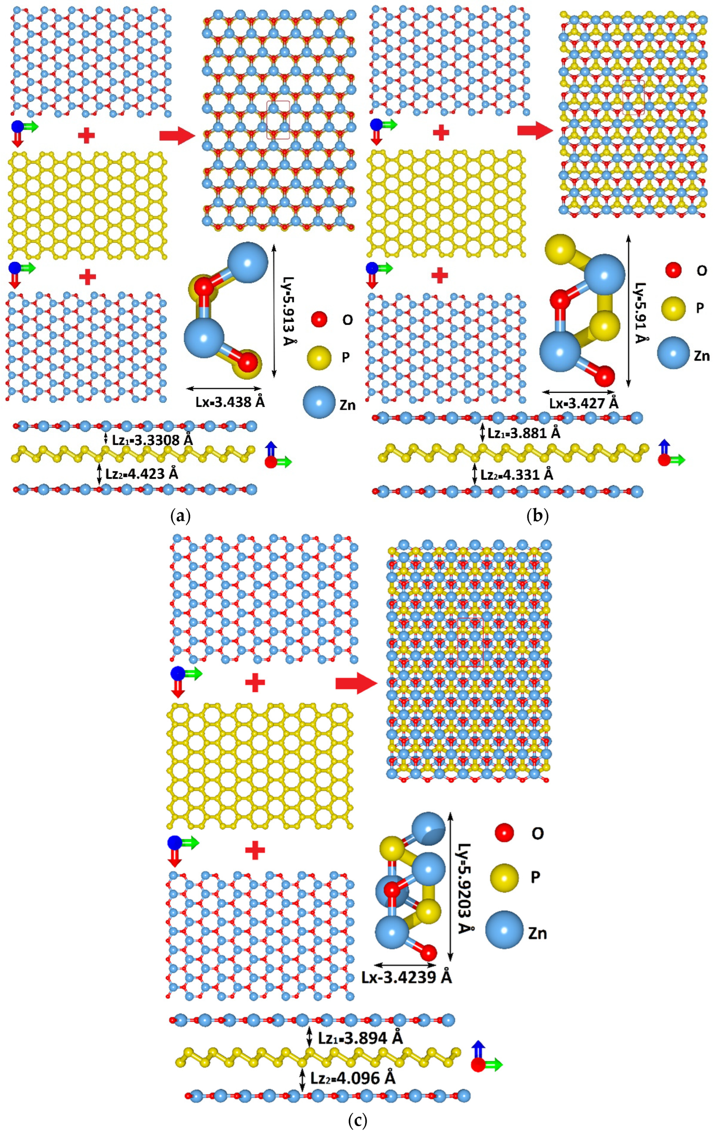
3.1. Atomistic Models of van der Waals ZnO/BlueP/ZnO Heterostructure

In this paper, we considered three-layer van der Waals heterostructures based on 2D monolayers of blue phosphorus and zinc oxide. Three types of packing of layers were considered for zinc oxide/blue phosphorus/zinc oxide (ZnO/BlueP/ZnO) heterostructure: (1) AAA type, in which the shift between layers is absent; (2) ABA type, in which the second layer is offset from the first; (3) ABC type, in which the second and third layers are shifted from the first layer. To minimize the lattice mismatch between the combined monolayers of blue phosphorus and zinc oxide, the sizes of the unit cells of each monolayer were increased until the difference in the parameters of the lattice vectors was no more than 2–3%. Figure 1 shows the process of stacking up monolayers during the formation of the ZnO/BlueP/ZnO heterostructure with AAA, ABA, and ABC stacking configurations. Additionally, this figure demonstrates unit cell of heterostructure with translations vectors Lx and Ly, and it indicates distance between layers along Z axis. The optimized values of the translation vectors of the supercell for the ZnO/BlueP/ZnO heterostructure with AAA stacking configurations were Lx = 3.438 Å and Ly = 5.913 Å; the distance between the upper layer of ZnO and BlueP along the Z axis was Lz1 = 3.330 Å, between the bottom layer of ZnO and BlueP was Lz2 = 4.423 Å. The optimized values of the translation vectors of the supercell for the ZnO/BlueP/ZnO heterostructure with ABA stacking configurations were Lx = 3.427 Å and Ly = 5.91 Å; the distance between the upper layer of ZnO and BlueP along the Z axis was Lz1 = 3.881 Å, between the bottom layer of ZnO and BlueP was Lz2 = 4.331 Å. The optimized values of the translation vectors of the supercell for the ZnO/BlueP/ZnO heterostructure with ABC stacking configurations were Lx = 3.423 Å and Ly = 5.920 Å; the distance between the upper layer of ZnO and BlueP along the Z axis was Lz1 = 3.894 Å, between the bottom layer of ZnO and BlueP was Lz2 = 4.096 Å.
For each of the constructed unit cells, an assessment of thermodynamic stability was carried out. Thermodynamic stability was estimated by changing the total energy of the studied heterostructure ΔE in accordance with the formula
Δ Ε = ( Ε V H Ε l a y e r s ) / N a t o m ,
where EVH is the energy of the vertical heterostructure, Elayers is the total energy of the layers that make up the heterostructure, Natom is the number of atoms in the heterostructure. The heterostructure was configured so that the total energy of the heterostructure in absolute value was less than that for individual 2D monolayers. According to our calculations, the change in energy during the formation of heterostructure was −317.23 eV/atom, which indicates a high energy stability of the heterostructure.

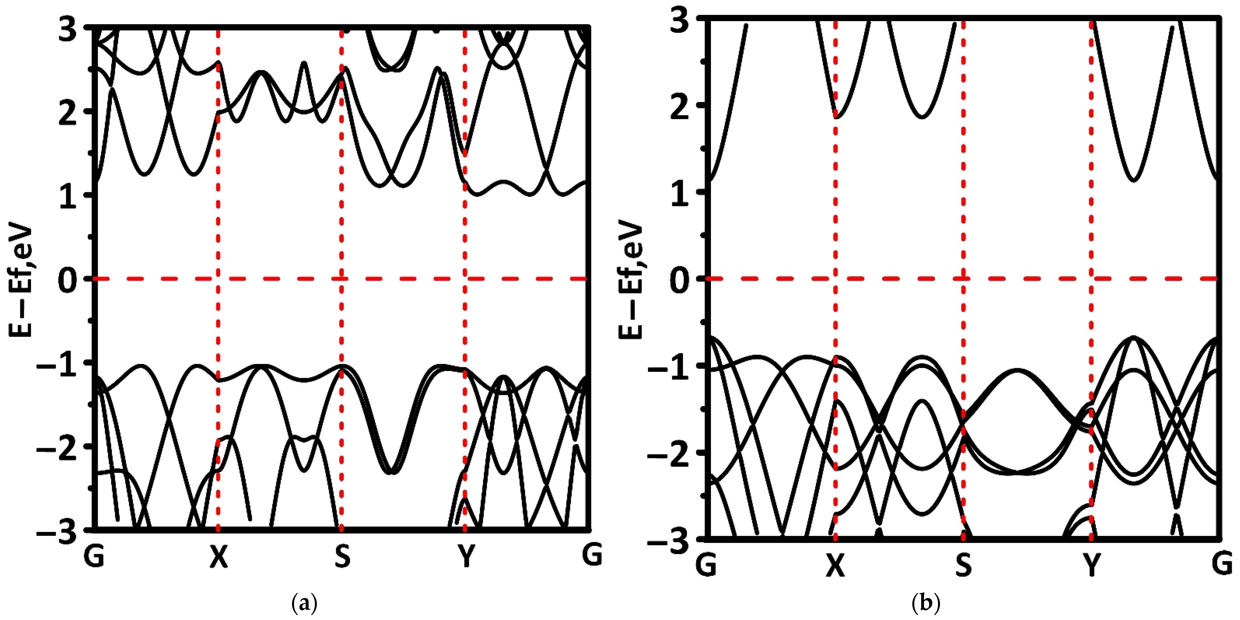
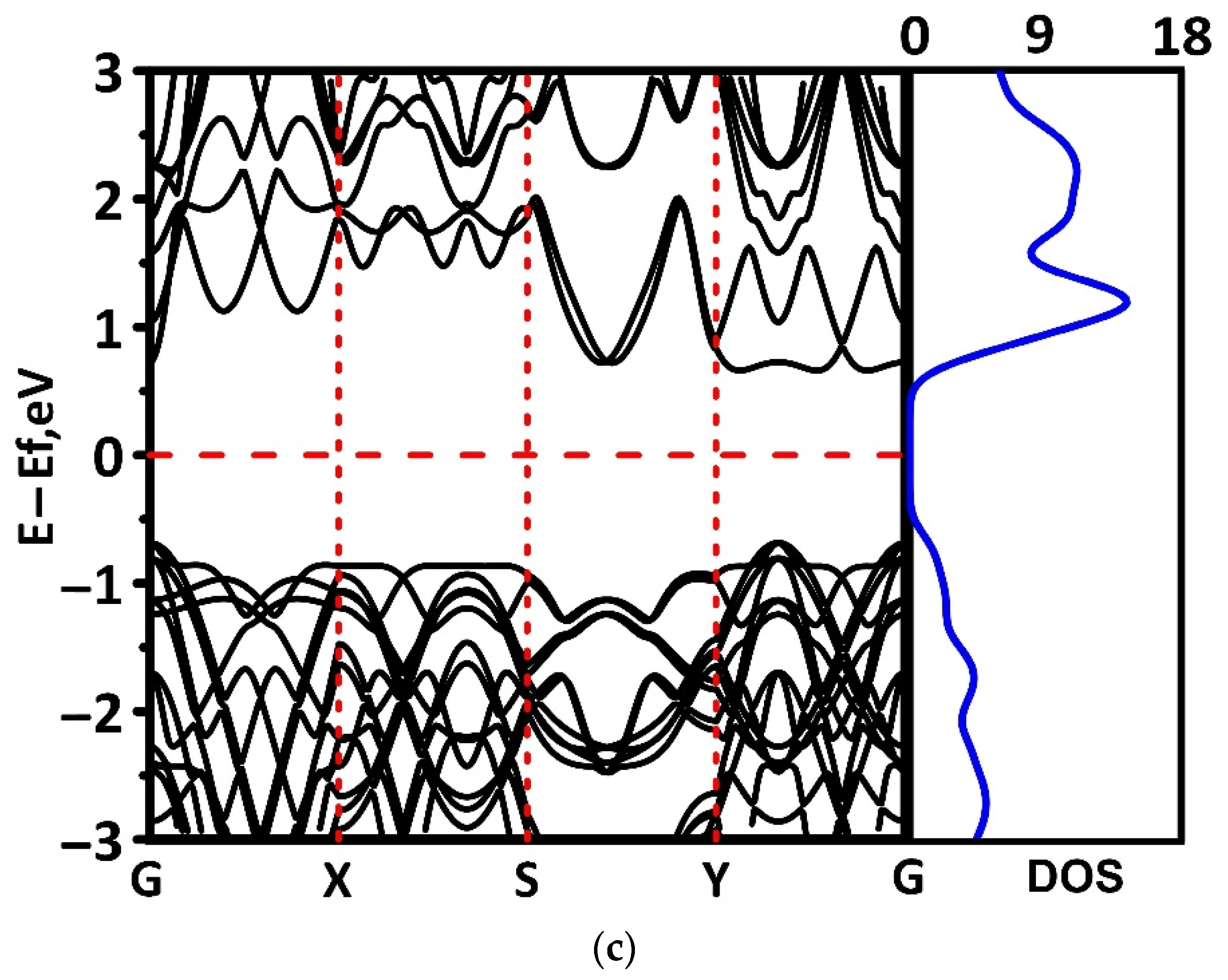
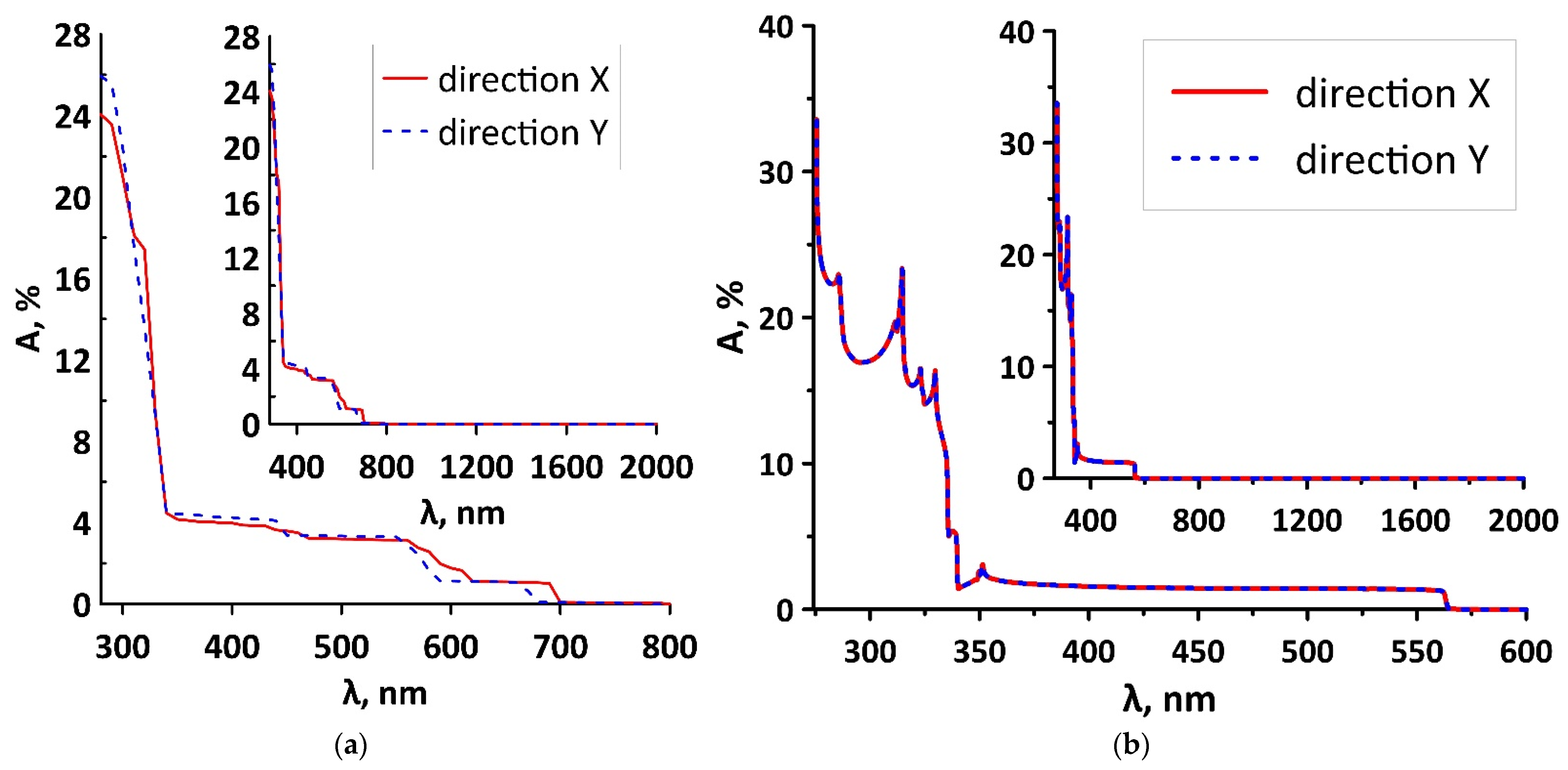
3.2. Electronic and Optical Properties

The band structure was calculated to reveal the regularities of the electronic structure of the studied layered 2D heterostructures. The structure of the first Brillouin zone was a rectangle with points of symmetry at the vertices G–X–S–Y–G. Based on the results of the calculation of the band structure, the distribution of the density of electronic states was constructed. Figure 2 demonstrates the obtained calculation results. The band structures are constructed in such a way as to represent the subbands near the Fermi level EF between all points of symmetry of the Brillouin zone. The Fermi level is shown by a dashed horizontal line passing through zero. It can be seen from this figure that ZnO/BlueP/ZnO heterostructure is semiconductor for all types of packing layers with an energy gap Eg = 0.70–0.75 eV: Eg = 0.75 eV for AAA-stacked ZnO/BlueP/ZnO heterostructure, Eg = 0.70 eV for ABA-stacked ZnO/BlueP/ZnO heterostructure, and Eg = 0.72 eV for ABC-stacked ZnO/BlueP/ZnO heterostructure. The presence of an energy gap in the considered three-layer heterostructures can be explained by the semiconducting conductivity of 2D monolayers of the zinc oxide (Eg = 3.4 eV) [50] and blue phosphorus (Eg = 1.93 eV) [51] forming the heterostructure. It should be noted that, near the bottom of the conduction band, the parabolic dispersion relation is observed both in the kx (G–X, S–Y) direction and in the ky (X–S, Y–G) direction. In this case, both the energy band profile and the DOS profile in these directions coincide for the three considered configurations of the ZnO/BlueP/ZnO heterostructure. Near the top of the valence band, differences in the energy dispersion between the types of layer packing in heterostructure are noticeable in the kx (G–X, S–Y) direction, which also manifests itself in the DOS profiles. In the X–S direction, the energy bands that form the top of the valence band are flat, which corresponds to a larger effective mass of charge carriers in this direction.
To determine the contribution of the monolayers that make up the ZnO/BlueP/ZnO heterosturcture, Figure 3 shows fragments of the band structure near the Fermi level for ZnO and BlueP monolayers. Comparing the band structures in Figure 2 and Figure 3, it can be noted that in the kx direction (G–X,S–Y), the electronic states of the BlueP monolayer make the decisive contribution to the formation of the band structure, whereas in the ky direction (X–S,Y–G), the decisive contribution is made by the electronic states of the ZnO monolayer.
To assess the optical properties of the ZnO/BlueP/ZnO heterostructure, the dynamic conductivity spectra were calculated in the wavelength range of 200–2000 nm. Two cases of electromagnetic wave polarization were considered: (1) the wave is polarized along the X axis in the plane of the 2D layer along the extended edge of the supercell; (2) the wave is polarized along the Y axis in the plane of the 2D layer across the extended edge of the supercell. Figure 4 shows the calculated profiles of dynamic conductivity spectra for van der Waals ZnO/BlueP/ZnO heterostructure with AAA, ABA, and ABC stacking configurations. In order to reveal the regularities of the formation of the profile of the dynamic conductivity of the ZnO/BlueP/ZnO heterostructure, the spectra of the dynamic conductivity of individual monolayers were calculated. They are shown in Figure 5.
Figure 4 and Figure 5 show that the profile of the dynamic conductivity spectrum of the ZnO/BlueP/ZnO heterostructure largely repeats the profiles of the spectrum of BlueP monolayer (in both cases of polarization along the X and Y axes). The characteristic features of this spectrum are the presence of a pronounced peak with a height of ~30σ00 is the conductivity quantum) at a wavelength of about 300 nm, a stepwise decrease in conductivity in the wavelength range of 300–700 nm, and a complete absence of conductivity in the wavelength range of 700–2000 nm. One can suggest that it is the BlueP semiconductor monolayer that makes the greatest contribution to the formation of the dynamical conductivity spectrum of ZnO/BlueP/ZnO heterostructure. This is indicated by the fact that, for the ZnO/BlueP/ZnO heterostructure, conductivity anisotropy is observed at different directions of wave polarization, as well as for blue phosphorus. At the same time, in the case of wave polarization along the X axis, the conductivity of zinc oxide is zero throughout wavelength range 200–2000 nm. It is shown that the type of layer packing has a weak effect on the profile of the conductivity spectrum. For the cases of AAA and ABA types of layer packing, the spectral profiles almost completely coincide. In the case of ABC type, with wave polarization along the Y axis, the maximum conductivity peak splits into two peaks of equal intensity located at 240 nm and 320 nm. In the cases of AAA and ABA types, the peak is located at a wavelength of 280 nm.
For the studied configurations of the ZnO/BlueP/ZnO heterostructure, the absorption spectra of electromagnetic waves were calculated in the range of 200–2000 nm. It has been established that for each configuration, the profile of the absorption spectrum repeats the profile of the optical conductivity spectrum, both when the wave is polarized along the X axis and when the wave is polarized along the Y axis. In all cases, the absorption maximum (about 26%) falls at a wavelength of 280 nm (middle ultraviolet). Starting from a wavelength of 700 nm, there is a complete absence of absorption. It is also possible to note the isotropy of absorption for different types of wave polarization. These features of the absorption spectrum are due to the optical properties of blue phosphorus, the absorption spectrum of which completely repeats the profile of the absorption spectrum of the ZnO/BlueP/ZnO heterostructure. In general, it can be noted that the type of layer packing does not affect the absorption spectrum of the ZnO/BlueP/ZnO heterostructure; therefore, Figure 6a shows the absorption spectrum for only one of the ZnO/BlueP/ZnO configurations, namely, with the AAA layer packing type. Figure 6b shows the absorption spectrum of the BlueP monolayer.

4. Conclusions

Thus, in this work, the possibility of creating a three-layer van der Waals heterostructure based on 2D monolayers of BlueP and ZnO was theoretically predicted. The results of calculating the formation energy of layered 2D structures showed that the proposed ZnO/BlueP/ZnO van der Waals heterostructure with AAA, ABA, and ABC stacking configurations has high thermodynamic stability, and, therefore, can be synthesized in a real experiment. At the same time, as compared with the known configurations of the bilayer ZnO/BlueP heterostructure [40,41,42], the thermodynamic stability of the three-layer ZnO/BlueP/ZnO structure increased hundreds of times. An analysis of the band structure of the constructed atomistic models showed that the ZnO/BlueP/ZnO heterostructure is an indirect-gap semiconductor with an energy gap of ~0.7 eV. The presence of one more ZnO monolayer made it possible to control the size of the energy gap, namely, to achieve its narrowing by 2–3 times in comparison with bilayer ZnO/BlueP heterostructures [40,42]. Considering the high sensitivity of the dynamic conductivity and absorbance coefficient of this structure to electromagnetic radiation in the wavelength range of 250–300 nm, it can be assumed that van der Waals ZnO/BlueP/ZnO heterostructures are promising for use in middle ultraviolet photodetectors as compared to bilayer ZnO/BlueP heterostructures, which have absorption peak in the visible and near ultraviolet region [41,42]. It can be assumed that such detectors will be highly efficient, since both heterostructures are practically insensitive to other wavelengths.

Author Contributions

Conceptualization, M.M.S. and O.E.G.; methodology, M.M.S. and O.E.G.; funding acquisition, M.M.S.; investigation, O.E.G., D.A.K. and M.M.S.; writing—original draft preparation, D.A.K. and M.M.S.; writing—review and editing, O.E.G. All authors have read and agreed to the published version of the manuscript.

Funding

The research was funded by Russian Science Foundation, grant number 21-72-00082.

Data Availability Statement

Not applicable.

Conflicts of Interest

The authors declare no conflict of interest.

References

  1. Novoselov, K.S.; Mishchenko, A.; Carvalho, A.; Castro Neto, A.H. 2D materials and van der Waals heterostructures. Science 2016, 353, aac9439. [Google Scholar] [CrossRef] [Green Version]
  2. Castellanos-Gomez, A. Why all the fuss about 2D semiconductors. Nat. Photonics 2016, 10, 202–204. [Google Scholar] [CrossRef] [Green Version]
  3. Liu, M.; Yin, X.; Ulin-Avila, E.; Geng, B.; Zentgraf, T.; Ju, L.; Wang, F.; Zhang, X. A graphene-based broadband optical modulator. Nature 2011, 474, 64–67. [Google Scholar] [CrossRef] [PubMed]
  4. Furchi, M.; Urich, A.; Pospischil, A.; Lilley, G.; Unterrainer, K.; Detz, H.; Klang, P.; Andrews, A.M.; Schrenk, W.; Strasser, G.; et al. Microcavity-integrated graphene photodetector. Nano Lett. 2012, 12, 2773–2777. [Google Scholar] [CrossRef]
  5. Eda, G.; Maier, S.A. Two-dimensional crystals: Managing light for optoelectronics. ACS Nano 2013, 7, 5660–5665. [Google Scholar] [CrossRef]
  6. Xia, F.; Wang, H.; Xiao, D.; Ramasubramaniam, A. Two-dimensional material nanophotonics. Nat. Photonics 2014, 8, 899–907. [Google Scholar] [CrossRef]
  7. Geim, A.K.; Grigorieva, I.V. Van der Waals heterostructures. Nature 2013, 499, 419–425. [Google Scholar] [CrossRef]
  8. Duong, D.L.; Yun, S.J.; Lee, Y.H. van der Waals Layered Materials: Opportunities and Challenges. ACS Nano 2017, 11, 11803–11830. [Google Scholar] [CrossRef]
  9. Yao, J.; Yang, G. Van der Waals heterostructures based on 2D layered materials: Fabrication, characterization, and application in photodetection. J. Appl. Phys. 2022, 131, 161101. [Google Scholar] [CrossRef]
  10. Nguyen, B.H.; Nguyen, V.H. Two-dimensional hexagonal semiconductors beyond graphene. Adv. Nat. Sci. Nanosci. Nanotechnol. 2016, 7, 043001. [Google Scholar] [CrossRef]
  11. Choi, W.; Choudhary, N.; Han, G.H.; Park, J.; Akinwande, D.; Lee, Y.H. Recent development of two-dimensional transition metal dichalcogenides and their applications. Mater. Today 2017, 20, 116–130. [Google Scholar] [CrossRef]
  12. Bellus, M.Z.; Li, M.; Lane, S.D.; Ceballos, F.; Cui, Q.; Zeng, X.C.; Zhao, H. Type-I van der Waals heterostructure formed by MoS2 and ReS2 monolayers. Nanoscale Horiz. 2017, 2, 31–36. [Google Scholar] [CrossRef] [PubMed]
  13. Hong, X.; Kim, J.; Shi, S.F.; Zhang, Y.; Jin, C.; Sun, Y.; Tongay, S.; Wu, J.; Zhang, Y.; Wang, F. Ultrafast charge transfer in atomically thin MoS2/WS2 heterostructures. Nat. Nanotechnol. 2014, 9, 682–686. [Google Scholar] [CrossRef] [Green Version]
  14. Gong, Y.; Lin, J.; Wang, X.; Shi, G.; Lei, S.; Lin, Z.; Zou, X.; Ye, G.; Vajtai, R.; Yakobson, B.I.; et al. Vertical and in-plane heterostructures from WS2/MoS2 monolayers. Nat. Mater. 2014, 13, 1135–1142. [Google Scholar] [CrossRef] [Green Version]
  15. Yu, Y.; Hu, S.; Su, L.; Huang, L.; Liu, Y.; Jin, Z.; Purezky, A.A.; Geohegan, D.B.; Kim, K.W.; Zhang, Y.; et al. Equally efficient interlayer exciton relaxation and improved absorption in epitaxial and nonepitaxial MoS2/WS2 heterostructures. Nano Lett. 2015, 15, 486–491. [Google Scholar] [CrossRef] [Green Version]
  16. Jiang, X.; Chen, F.; Zhao, S.; Su, W. Recent progress in the CVD growth of 2D vertical heterostructures based on transition-metal dichalcogenides. CrystEngComm 2021, 23, 8239–8254. [Google Scholar] [CrossRef]
  17. Chen, Y.; Jia, B.; Guan, X.; Han, L.; Wu, L.; Guan, P.; Lu, P. Design and analysis of III-V two-dimensional van der Waals heterostructures for ultra-thin solar cells. Appl. Surf. Sci. 2022, 586, 152799. [Google Scholar] [CrossRef]
  18. Britnell, L.; Gorbachev, R.V.; Jalil, R.; Belle, B.D.; Schedin, F.; Mishchenko, A.; Georgiou, T.; Katsnelson, M.I.; Eaves, L.; Morozov, S.V.; et al. Field-effect tunneling transistor based on vertical graphene heterostructures. Science 2012, 335, 947–950. [Google Scholar] [CrossRef] [Green Version]
  19. Chen, C.C.; Li, Z.; Shi, L.; Cronin, S.B. Thermoelectric transport across graphene/hexagonal boron nitride/graphene heterostructures. Nano Res. 2015, 8, 666–672. [Google Scholar] [CrossRef]
  20. Withers, F.; Del Pozo-Zamudio, O.; Mishchenko, A.; Rooney, A.P.; Gholinia, A.; Watanabe, K.; Taniguchi, T.; Haigh, S.J.; Geim, A.K.; Tartakovskii, A.I.; et al. Light-emitting diodes by band-structure engineering in van der Waals heterostructures. Nat. Mater. 2015, 14, 301–306. [Google Scholar] [CrossRef]
  21. Li, X.; Lin, S.; Lin, X.; Xu, Z.; Wang, P.; Zhang, S.; Zhong, H.; Xu, W.; Wu, Z.; Fang, W. Graphene/h-BN/GaAs sandwich diode as solar cell and photodetector. Opt. Express 2016, 24, 134–145. [Google Scholar] [CrossRef]
  22. Mawwa, J.; Shamim, S.; Khanom, S.; Hossain, M.K.; Ahmed, F. In-plane graphene/boron nitride heterostructures and their potential application as toxic gas sensors. RSC Adv. 2021, 11, 32810–32823. [Google Scholar] [CrossRef]
  23. Yu, L.; Lee, Y.H.; Ling, X.; Santos, E.J.; Shin, Y.C.; Lin, Y.; Dubey, M.; Kaxiras, E.; Kong, J.; Wang, H.; et al. Graphene/MoS2 hybrid technology for large-scale two-dimensional electronics. Nano Lett. 2014, 14, 3055–3063. [Google Scholar] [CrossRef] [Green Version]
  24. Wang, J.; Ma, F.; Sun, M. Graphene, hexagonal boron nitride, and their heterostructures: Properties and applications. RSC Adv. 2017, 7, 16801–16822. [Google Scholar] [CrossRef] [Green Version]
  25. Li, G.; Zhang, L.; Xu, W.; Pan, J.; Song, S.; Zhang, Y.; Zhou, H.; Wang, Y.; Bao, L.; Zhang, Y.Y.; et al. Stable Silicene in Graphene/Silicene Van der Waals Heterostructures. Adv. Mater. 2018, 30, e1804650. [Google Scholar] [CrossRef]
  26. Mudd, G.W.; Svatek, S.A.; Hague, L.; Makarovsky, O.; Kudrynskyi, Z.R.; Mellor, C.J.; Beton, P.H.; Eaves, L.; Novoselov, K.S.; Kovalyuk, Z.D.; et al. High broad-band photoresponsivity of mechanically formed InSe-graphene van der Waals heterostructures. Adv. Mater. 2015, 27, 3760–3776. [Google Scholar] [CrossRef] [Green Version]
  27. Zhang, K.; Zhang, T.; Cheng, G.; Li, T.; Wang, S.; Wei, W.; Zhou, X.; Yu, W.; Sun, Y.; Wang, P.; et al. Interlayer Transition and Infrared Photodetection in Atomically Thin Type-II MoTe2/MoS2 van der Waals Heterostructures. ACS Nano 2016, 10, 3852–3858. [Google Scholar] [CrossRef] [PubMed]
  28. Kaur, S.; Kumar, A.; Srivastava, S.; Tankeshwar, K. van der Waals heterostructures based on allotropes of phosphorene and MoSe2. Phys. Chem. Chem. Phys. 2017, 19, 22023–22032. [Google Scholar] [CrossRef] [Green Version]
  29. Tian, H.; Chin, M.L.; Najmaei, S.; Guo, Q.; Xia, F.; Wang, H.; Dube, M. Optoelectronic devices based on two-dimensional transition metal dichalcogenides. Nano Res. 2016, 9, 1543–1560. [Google Scholar] [CrossRef]
  30. Chen, Y.; Wang, Y.; Wang, Z.; Gu, Y.; Ye, Y.; Chai, X.; Ye, J.; Chen, Y.; Xie, R.; Zhou, Y.; et al. Unipolar barrier photodetectors based on van der Waals heterostructures. Nat. Electron. 2021, 4, 357–363. [Google Scholar] [CrossRef]
  31. Li, Q.; Meng, J.; Li, Z. Recent progress on Schottky sensors based on two-dimensional transition metal dichalcogenides. J. Mater. Chem. A 2022, 10, 8107–8128. [Google Scholar] [CrossRef]
  32. Jia, Z.; Li, S.; Xiang, J.; Wen, F.; Bao, X.; Feng, S.; Yang, R.; Liu, Z. Highly sensitive and fast monolayer WS2 phototransistors realized by SnS nanosheet decoration. Nanoscale 2017, 9, 1916–1924. [Google Scholar] [CrossRef]
  33. Yoo, G.; Choi, S.; Park, S.; Lee, K.T.; Lee, S.; Oh, M.S.; Heo, J.; Park, H.J. Flexible and Wavelength-Selective MoS2 Phototransistors with Monolithically Integrated Transmission Color Filters. Sci. Rep. 2017, 7, 40945. [Google Scholar] [CrossRef] [Green Version]
  34. Huo, N.J.; Yang, Y.J.; Li, J.B. Optoelectronics based on 2D TMDs and heterostructures. J. Semicond. 2017, 38, 031002. [Google Scholar] [CrossRef]
  35. Wang, F.; Wang, Z.; Yin, L.; Cheng, R.; Wang, J.; Wen, Y.; Shifa, T.A.; Wang, F.; Zhang, Y.; Zhan, X.; et al. 2D library beyond graphene and transition metal dichalcogenides: A focus on photodetection. Chem. Soc. Rev. 2018, 47, 6296–6341. [Google Scholar] [CrossRef]
  36. Zou, Y.; Zhang, Y.; Hu, Y.; Gu, H. Ultraviolet Detectors Based on Wide Bandgap Semiconductor Nanowire: A Review. Sensors 2018, 18, 2072. [Google Scholar] [CrossRef] [Green Version]
  37. Mannix, A.J.; Zhou, X.F.; Kiraly, B.; Wood, J.D.; Alducin, D.; Myers, B.D.; Liu, X.; Fisher, B.L.; Santiago, U.; Guest, J.R.; et al. Synthesis of borophenes: Anisotropic, two-dimensional boron polymorphs. Science 2015, 350, 1513–1516. [Google Scholar] [CrossRef] [Green Version]
  38. Feng, B.; Zhang, J.; Zhong, Q.; Li, W.; Li, S.; Li, H.; Cheng, P.; Meng, S.; Chen, L.; Wu, K. Experimental realization of two-dimensional boron sheets. Nat. Chem. 2016, 8, 563–568. [Google Scholar] [CrossRef] [Green Version]
  39. Golias, E.; Krivenkov, M.; Varykhalov, A.; Sánchez-Barriga, J.; Rader, O. Band Renormalization of Blue Phosphorus on Au(111). Nano Lett. 2018, 18, 6672–6678. [Google Scholar] [CrossRef] [Green Version]
  40. Li, X.; Wu, X.; Zhu, Z.; Li, G.; Mi, C. On the elasticity and piezoelectricity of black(blue) phosphorus/ZnO van der Waals heterostructures. Comput. Mater. Sci. 2019, 169, 109134. [Google Scholar] [CrossRef]
  41. Li, B.; Zhang, S.F.; Ji, W.X.; Zhang, C.W.; Li, P.; Wang, P.J. The electric-field and strain inducing electronic and optical properties of the blue phosphorene/ZnO heterostructures. Phys. E Low-Dimens. Syst. Nanostructures 2020, 115, 113650. [Google Scholar] [CrossRef]
  42. Niu, X.; Li, Y.; Shu, H.; Yao, X.; Wang, J. Efficient Carrier Separation in Graphitic Zinc Oxide and Blue Phosphorus van der Waals Heterostructure. J. Phys. Chem. C 2017, 121, 3648–3653. [Google Scholar] [CrossRef]
  43. Momeni, K.; Ji, Y.; Wang, Y.; Paul, S.; Neshani, S.; Yilmaz, D.E.; Shin, Y.K.; Zhang, D.; Jiang, J.W.; Park, H.S.; et al. Multiscale computational understanding and growth of 2D materials: A review. Npj Comput. Mater. 2020, 6, 22. [Google Scholar] [CrossRef] [Green Version]
  44. Soler, J.M.; Artacho, E.; Gale, J.D.; García, A.; Junquera, J.; Ordejón, P.; Sánchez-Portal, D. The SIESTA method for ab-initio order-N materials simulation. J. Phys. Condens. Matt. 2002, 14, 2745–2779. [Google Scholar] [CrossRef] [Green Version]
  45. The SIESTA Group. Available online: Departments.icmab.es/leem/siesta/ (accessed on 10 April 2021).
  46. Perdew, J.P.; Chevary, J.A.; Vosko, S.H.; Jackson, K.A.; Pederson, M.R.; Singh, D.J.; Fiolhais, C. Atoms, molecules, solids, and surfaces: Applications of the generalized gradient approximation for exchange and correlation. Phys. Rev. B 1992, 46, 6671–6687. [Google Scholar] [CrossRef]
  47. Berland, K.; Hyldgaard, P. Exchange functional that tests the robustness of the plasmon description of the van der Waals density functional. Phys. Rev. B 2014, 89, 035412. [Google Scholar] [CrossRef] [Green Version]
  48. Monkhorst, H.J.; Pack, J.D. Special points for Brillouin-zone integrations. Phys. Rev. B 1976, 13, 5188–5192. [Google Scholar] [CrossRef]
  49. Economou, E.N. Green’s Functions in Quantum Physics, 2nd ed.; Springer: Berlin/Heidelberg, Germany, 1983; pp. 55–75. [Google Scholar]
  50. Chen, L.L.; Cui, Y.; Xiong, Z.; Zhou, M.; Gao, Y. Chemical functionalization of the ZnO monolayer: Structural and electronic properties. RSC Adv. 2019, 9, 21831–21843. [Google Scholar] [CrossRef] [Green Version]
  51. Li, B.; Ren, C.; Zhang, S.; Ji, W.; Zhang, C.; Li, P.; Wang, P. Electronic Structural and Optical Properties of Multilayer Blue Phosphorus: A First-Principle Study. J. Nanomater. 2019, 2019, 4020762. [Google Scholar] [CrossRef]
Figure 1. The process of constructing atomistic model of van der Waals ZnO/BlueP/ZnO heterostructure with AAA (a), ABA (b), and ABC (c) stacking configurations.
Jcs 06 00163 g001
Figure 2. Band structure and DOS of van der Waals ZnO/BlueP/ZnO heterostructure with AAA (a), ABA (b), and ABC (c) stacking configurations.
Jcs 06 00163 g002aJcs 06 00163 g002b
Figure 3. Band structure of BlueP (a) and ZnO (b) monolayers.
Jcs 06 00163 g003
Figure 4. The dynamic conductivity spectra of van der Waals ZnO/BlueP/ZnO heterostructure with AAA (a), ABA (b), and ABC (c) stacking configurations for two cases of electromagnetic wave polarization (along the X and Y axes).
Jcs 06 00163 g004
Figure 5. The dynamic conductivity spectra of monolayers of BlueP (a) and ZnO (b) monolayers for two cases of electromagnetic wave polarization (along the X and Y axes).
Jcs 06 00163 g005
Figure 6. The absorbance spectra of van der Waals ZnO/BlueP/ZnO heterostructure with AAA stacking configuration (a) and BlueP monolayer (b) for two cases of electromagnetic wave polarization (along the X and Y axes).
Jcs 06 00163 g006
Publisher’s Note: MDPI stays neutral with regard to jurisdictional claims in published maps and institutional affiliations.

