Article

Ion Beam Effect on the Structural and Optical Properties of AlN:Er

1
College of Nuclear Science and Technology, Harbin Engineering University, Harbin 150400, China
2
Experimental Physics Division, National Center for Physics, Islamabad 44000, Pakistan
3
Department of Textile Engineering, Balochista University of Information Technology, Engineering, and Management Sciences, Quetta 87800, Pakistan
4
College of Material Science and Chemical Engineering, Harbin Engineering University, Harbin 150400, China
5
Department of Clinical & Diagnostic Sciences, The University of Alabama at Birmingham, Birmingham, AL 35294, USA
*
Author to whom correspondence should be addressed.
J. Compos. Sci. 2022, 6(4), 110; https://doi.org/10.3390/jcs6040110
Submission received: 22 February 2022 / Revised: 27 March 2022 / Accepted: 1 April 2022 / Published: 7 April 2022
(This article belongs to the Special Issue Feature Papers in Journal of Composites Science in 2022)

Abstract

:
Erbium (Er)-doped Aluminum Nitride (AlN) thin films were deposited and fabricated on Si (100) and Si (111) substrates in a Nitrogen atmosphere using the plasma magnetron sputtering technique. The deposited and fabricated thin films were thermally annealed at 900 °C in Argon (Ar) atmosphere. The samples were irradiated with protons at a dose of 1 × 10¹⁴ ions/cm2 which carried an incident energy of 335 keV, using a tandem pelletron accelerator. Rutherford backscattering spectroscopy (RBS) and X-ray diffraction (XRD) were used for the stoichiometric and structural analysis of the films, while Fourier transforms infrared spectroscopy (FTIR) was performed to track the changes in the optical characteristics of thin films before and after the ions’ irradiation and implantation. The irradiation has affected the optical and structural properties of the films, which could be exploited to use the AlN:Er films for various optoelectronic and solid-state device applications.

1. Introduction

AlN is considered a fascinating candidate in power generation devices due to its high bandgap [1,2,3,4,5,6]. The direct bandgap of 6.12 eV (at room temperature), the thermal conductivity of 321 W/(mK) [7], and the electrical insulator are some of its attractive features. Tuning the properties of a material as desired can be achieved via different physical and chemical treatments such as the doping of impurities, ions implantation [8], thermal annealing [9] or functional group attachment [10], etc. It has previously been reported that rare earth (RE) doped impurities have a significant impact on the optical behavior of AlN. This is because the doping of these impurities results in changes in structural properties due to atomic size mismatch and provides recombination centers for the photoluminescence, owing to 4f orbitals of RE [11]. The material undergoes a sharp emission when excited. The application of such modified thin-film semiconductors includes but is not limited to solid-state devices, memory storage, flat panel displays, and high-resolution printing. Other than these domains, the implanted or the doped specimens can also be used in aerospace technology, high power devices, flame detection, petroleum industry, and under-sea communications [12,13]. Previously published works have shown that ion implantation/irradiation can be used to modify the electrical, structural, magnetic [14], optical, and piezoelectric [15,16]. Defect damages due to unexpected erosion as a function of temperature can also be expected with irradiation, depending on the magnitudes of physical parameters used during ion bombardment [17,18].
In this work, we demonstrate the fabrication of AlN:Er thin films using the magnetron sputtering technique, followed by thermal annealing at a temperature of 900 °C (1173 K), and then a thorough investigation of the change in structural and optical properties induced by irradiation using RBS, FTIR, and XRD measurement techniques. Our work uniquely describes the effect of proton irradiation on the structural, electronic, and optical properties of sputtered AlN:Er films.

2. Materials and Methods

2.1. Thin Film Deposition

Growth of the thin films on a specific plane affects the crystallographic properties of the films, therefore we either cut along (100) or (111) plane of the single-crystal Si. At 300 K we deposited the sample using magnetron sputtering, as shown in Figure 1.
In Figure 1, Al, Er with Si substrate were used as the target, while Ar ions are the impinging ions deposited over the said targets which were placed on the anode. Al and Er atoms are sputtered by Ar ions, then Al reacts with N present in the atmosphere and is deposited as AlN on the Si substrate. The use of a magnet as shown in the schematic is to focus the beam of Ar ions. The system was powered electrically between 100 W and 200 W. An outlet in the deposition chamber was connected to a cryopump in order to create a vacuum. A 4 × 10⁻⁶ kPa vacuum was produced using the pump [19]. The pressure used during the operation was set to 3 × 10⁻⁵ Torr.
Thin films of AlN doped with Erbium (Er) were prepared by radio frequency (rf) magnetron sputtering of aluminum targets of 99.999% purity in a pure nitrogen atmosphere. Doping of the thin films bilayer with Er was accomplished by drilling small holes (3/16 in. diameter) in the aluminum targets and placing a slug of Er in the holes separately. Erbium was then co-sputtered with the aluminum.
Bilayer films were deposited by using two targets and using them alternatively by flipping over the substrate [20].

2.2. Thin Film Characterizations
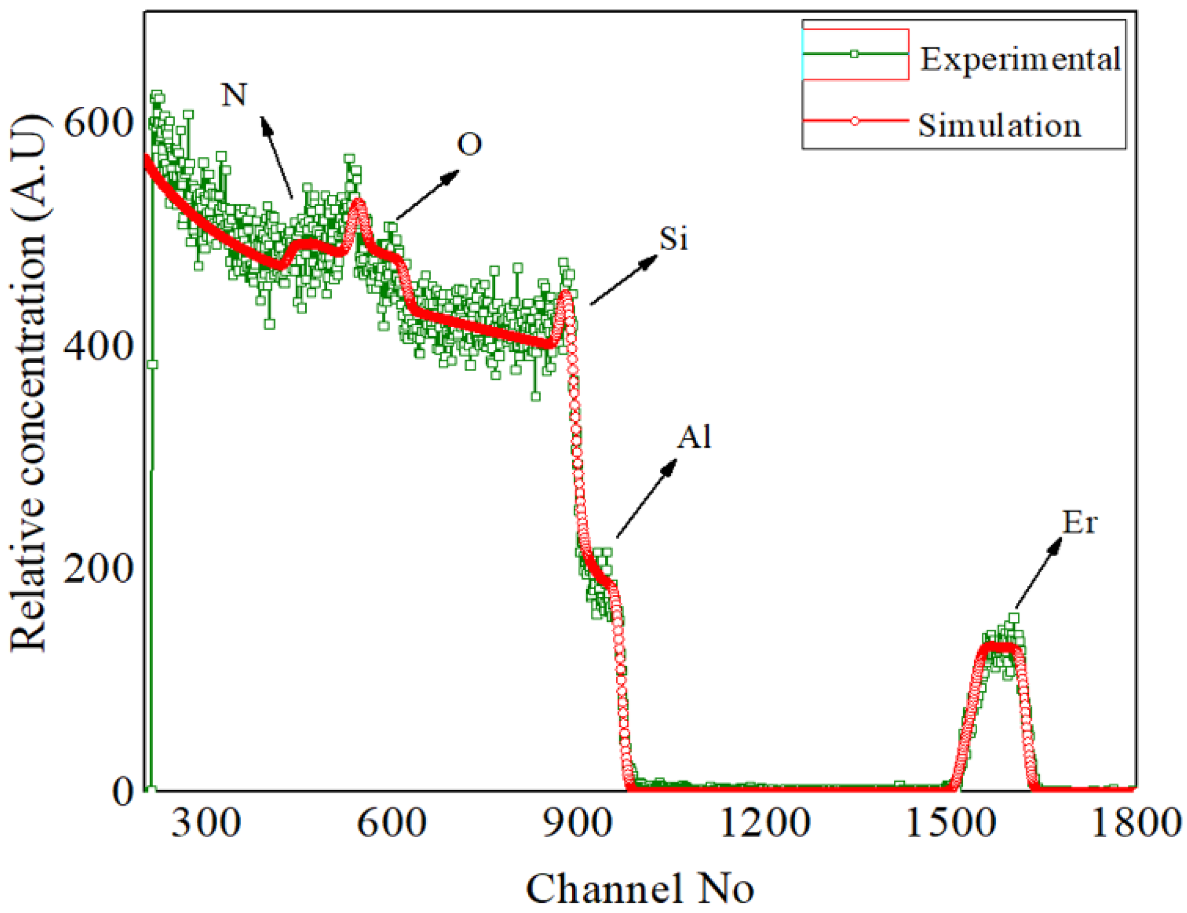
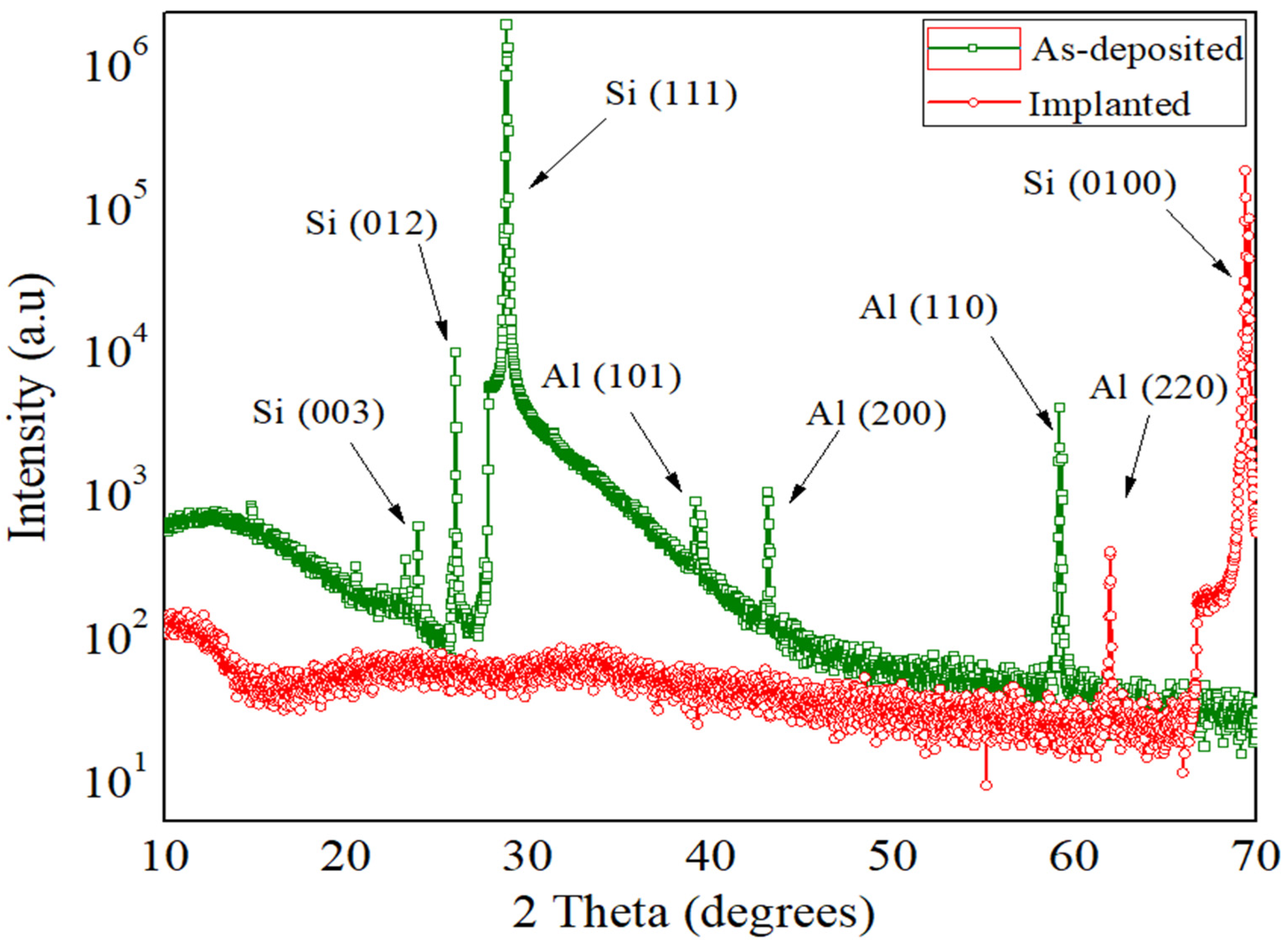
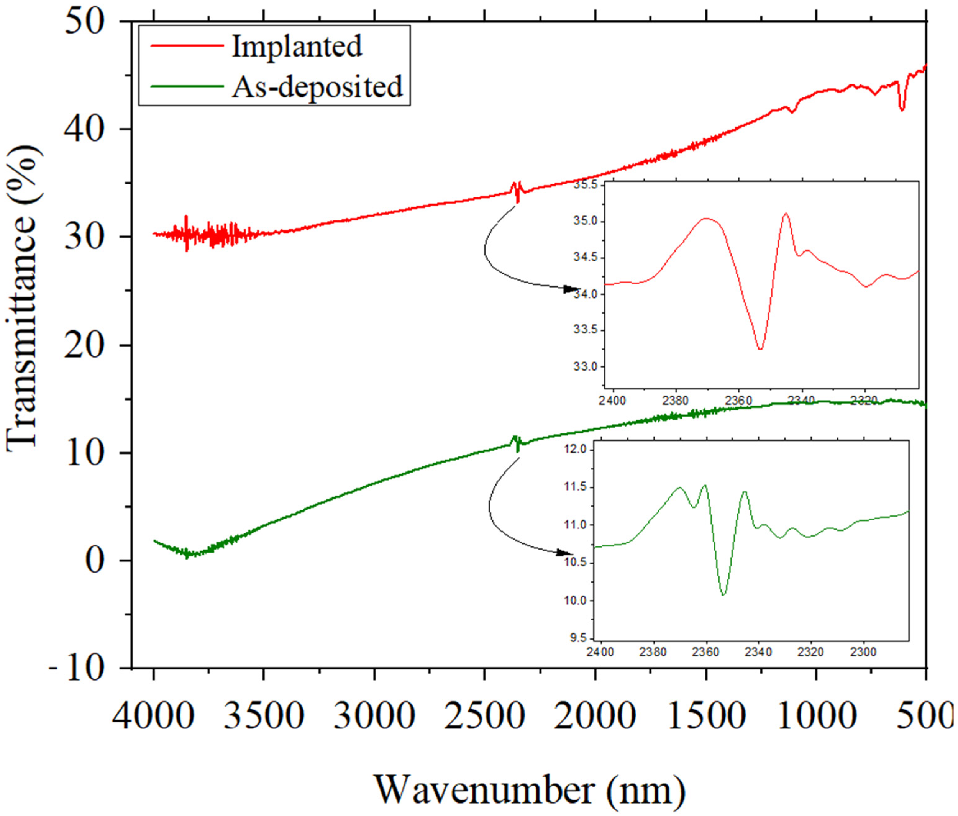
We cut a single piece of the as-prepared sample into two pieces and irradiated one piece among them, leaving behind the other un-irradiated. All the characterizations were performed at the national center for Physics (NCP), Quaid e Azam University, Islamabad, Pakistan. Before the irradiation, we annealed the samples thermally at a temperature of 900 °C. The dose and the energy of the incident proton beam used were 1 × 10¹⁴ ions/cm2 and 335 keV. Later, the samples were characterized for modification in properties upon irradiation by performing RBS, XRD, and FTIR. The RBS data was obtained for the samples, using a 5 MV Pelletron tandem accelerator (5UDH-2 Pelletron, National Electrostatic Corporation, Middleton, WI, USA). The XRD data were acquired on Bruker’s D8 Advance system using Cu Kα radiation (λ = 1.5406 Å) X-ray source, while the FTIR measurement was conducted by FT/IR-6600 type A model.

3. Results

RBS is an analytical technique that is normally used to acquire depth information profiling, elemental identification, and their relative concentrations (stoichiometry) in the target material [3,15]. The analysis is based on the ion solid interaction phenomenon where the lighter ions (typically protons or alpha) have acolumbic interaction with the target and backscattered containing the information about the material in the form of energy. The spectrum of RBS for the AlN:Er was obtained using a 2.0 MeV He++ beam used in a perpendicular direction to the surface area of the targets. The measured current of the He beam ranged from 26 to 36 nA, where the charge collection was 20 µC. The detector was held constant at its position at 170° to the beam of ions. In order to extract the film’s parameters from these results, a fitting of the experimental data was carried out using SIMNRA [21], with a detector resolution of 28 keV. Figure 2 illustrates in the green and red colors the experimental and computational curves, respectively obtained from the RBS analysis. The obtained results also provided the approximate thickness of the film to be ~160 nm. Since the Er ions have no penetration power (almost negligible incident energy) surface deposition will most likely occur. Moreover, oxygen has further been defused in the substrate forming a layer of silicon dioxide. Oxygen is an unwanted element that has been seen in the entire RBS spectrum, which may have been introduced in the AlN films during the deposition process as an impurity specie or after the completion of the deposition process and exposure to the air. The elemental composition and thickness of the films is shown in Table 1.
Irradiation causes the formation of point defects within the matrix of the targeted materials [22,23]. These defects agglomerates, form dislocations and voids alter first the structural and then the mechanical characteristics of the materials. AlN can be found in wurtzite, rocksalt, or Zinc blende structure [24,25], but the doping of Er due to size mismatch will have apparently perturbed their crystallinity. On the other hand, the irradiation will deteriorate it more. Therefore, the microstructure characterization was performed systematically by using XRD. A Cu Kα radiation (λ = 1.5406 Å) was directed onto the target to obtain information regarding the diffracted ray at room temperature, which will inform us about the structure of the films. Figure 3 compares the XRD spectra obtained for the deposited and implanted samples.
In Figure 3, the peaks at (012), (111), and (003) correspond to the planes of the Si substrate [26,27]. For Al, the identified peaks are (200), (110), and (110) [27]. As can be seen from the XRD curves, the existing peaks in the as-deposited film are replaced with some new peaks, i.e., Si [0100] [28] and Al [220] [29]. From the XRD measurements, it can be vividly seen that the impinged ions seriously affected the crystallinity of the samples. The number of peaks in the implanted sample was reduced and the intensity of diffracted light reduced, which confirmed that the ion-implanted film was amorphized in comparison to the as-deposited one.
FTIR measurements are used to monitor a change in the composition of the material or the presence of certain contamination of external elements through the absorption of infrared radiation in the samples. In our case, FTIR of the films was studied to observe the likely subsurface bonds formation, other than the impurities doped in AlN. The measurements were taken in transmittance mode and the wavenumber range was from 4000–500 cm−1.
In Figure 4, Al-N bonds are shown in the peak which ranges from 500 to 1000 cm−1 announcing the existence of the vibration mode for Al–N bonds, while the presence of small peaks in the range from 1050 to 1400 are representing stretching of them [30,31]. In the range of 2270–2420 cm−1 the peaks represent the CO2. This is supported by other authors who claimed that these peaks are not from the samples but contributed from the spectrometer to the FTIR spectra [32,33], while at 1105 cm−1 the absorption peak is attributed to Si–O stretching [34].

4. Conclusions

Thin films of AlN:Er were fabricated using a magnetron sputtering mechanism. Thermal annealing after the fabrication was performed at 900 °C. Protons were illuminated on the surface of the thin films using a tandem pelletron accelerator with an incident energy of 335 keV at a dose of 1 × 10¹⁴ ions/cm2. The composition of the thin films remained unchanged with the irradiation. It was concurred that the structural properties seriously vary with irradiation. New peaks were observed with the irradiation, such as Si (111), Al (110), Al (200), etc. No new bonding was observed with the FTIR analysis before and after the irradiation, which implies that no new elements have been formed with the proton irradiation. The transmittance increased with irradiation, which inferred changes in the transparency of the material.

Author Contributions

Conceptualization, A.H.S. (Altaf Hussain Shar), M.M. and M.U.; methodology, M.M.; software, A.U.; validation, M.U. and A.U.; formal analysis, A.U.; investigation, A.U.; resources, A.H.S. (Ahmer Hussain Shah), A.H.S. (Altaf Hussain Shar) and M.U.; data curation, A.H.S. (Ahmer Hussain Shah), A.U. and M.M.; writing—original draft preparation, A.U.; writing—review and editing, A.U. and M.M.; visualization, A.H.S. (Altaf Hussain Shar) and A.U.; supervision, M.U. and M.M.; project administration, M.U. and M.M. All authors have read and agreed to the published version of the manuscript.

Funding

The research received no funding.

Institutional Review Board Statement

Not applicable.

Informed Consent Statement

Not applicable.

Data Availability Statement

Data is contained within the article.

Conflicts of Interest

The authors declare no conflict of interest.

References

  1. Subramani, S.; Mutharasu, M. Influence of AlN Thin Film as Thermal Interface Material on Therminfal and Optical Properties of High-Power LED. IEEE Trans. Device Mater. Reliab. 2014, 14, 30–34. [Google Scholar] [CrossRef]
  2. Ponce, F.A.; Bour, D.P. Nitride-based semiconductors for blue and green light-emitting devices. Nature 1997, 386, 351–359. [Google Scholar] [CrossRef]
  3. Ullah, A.; Usman, M.; Qingyu, W.; Ahmad, I.; Khosa, R.Y.; Maqbool, M. Response of structural and optical properties against proton irradiation in AlN:Tm thin films. Radiat. Phys. Chem. 2021, 180, 109234. [Google Scholar] [CrossRef]
  4. Alsaad, A.M.; Al-Bataineh, Q.M.; Qattan, I.A.; Ahmad1, A.A.; Ababneh, A.; Albataineh, Z.; Aljarrah, I.A.; Telfah, A. Measurement and ab initio Investigation of Structural, Electronic, Optical, and Mechanical Properties of Sputtered Aluminum Nitride Thin Films. Front. Phys. 2020, 8, 115. [Google Scholar] [CrossRef]
  5. Mendez, M.G.; Rodrıguez, S.M.; Machorro, R.; de la Cruz, W. Characterization of ALN thin films deposited by DC reactive magnetron sputtering. Rev. Mex. Fis. 2008, 54, 271–278. [Google Scholar]
  6. Vaskin, A.; Kolkowski, R.; Koenderink, A.F.; Staude, I. Light-Emitting Metasurfaces: Simultaneous Control of Spontaneous Emission and Far-Field Radiation. Nanophotonics 2019, 8, 1151–1198. [Google Scholar] [CrossRef]
  7. Cheng, Z.; Koh, Y.R.; Mamun, A.; Shi, J.; Bai, T.; Huynh, K.; Yates, L.; Liu, Z.; Li, R.; Lee, E.; et al. Experimental observation of high intrinsic thermal conductivity of AlN. Phys. Rev. Mater. 2020, 4, 044602. [Google Scholar] [CrossRef]
  8. Ullah, A.; Usman, M.; Qingyu, W.; Ahmad, I.; Maqbool, M. Fabrication and ions irradiation study of AlN:Gd thin films ECS. J. Solid State Sci. Technol. 2022. [Google Scholar] [CrossRef]
  9. Liu, Y.; Lu, Q.; Lin, G.; Liu, J.; Lu, S.; Tang, Z.; He, H.; Fu, Y.; Shen, X. Effect of thermal annealing on properties of amorphous GaN/p-Si heterojunctions. Mater. Res. Express 2019, 6, 085904. [Google Scholar] [CrossRef]
  10. Zan, H.-W.; Chou, C.-W.; Wang, C.-H.; Song, H.-T.; Hwang, J.-C.; Lee, P.-T. Carbon attachment on the aluminum nitride gate dielectric in the pentacene-based organic thin-film transistors. J. Appl. Phys. 2009, 105, 063718. [Google Scholar] [CrossRef] [Green Version]
  11. Fang, L.; Yin, A.; Zhu, S.; Ding, J.; Chen, L.; Zhang, D.; Pu, Z.; Liu, T. On the potential of Er-doped AlN film as a luminescence sensing layer for multilayer Al/AlN coating health monitoring. J. Alloys Compd. 2017, 8, 174. [Google Scholar] [CrossRef]
  12. Favennec, P.N.; Haridon, H.L.; Salvi, M.; Moutonnet, D.; Guillou, Y.L. Electrical, optical, and magnetic properties of Erbium. Elect. Lett. 1989, 25, 718. [Google Scholar] [CrossRef]
  13. Wu, X.; Hmmerich, U.; MacKenzie, J.D.; Abernathy, C.R.; Pearton, S.J.; Wilson, R.G.; Schwartz, R.N.; Zavada, J.M. Photoluminescence study of Er-doped AlN. J. Lumin. 1997, 72–74, 284–286. [Google Scholar] [CrossRef]
  14. Hassan, N.; Hussain, Z.; Naeem, M.; Shah, I.A.; Husnain, G.; Ahmad, I.; Ullah, Z. Influence of Ion Beam Irradiation on Structural, Magnetic and Electrical Characteristics of Ho-doped AlN Thin Films. Surf. Rev. Lett. 2016, 10, 1142. [Google Scholar] [CrossRef]
  15. Ullah, A.; Wang, Q.; Ahmad, I.; Usman, M. Irradiation effects on Nd and W doped Aluminum Nitride thin films. Phys. B Cond. Mat. 2020, 586, 412086. [Google Scholar] [CrossRef]
  16. Usman, M.; Hallén, A.; Nazir, A. Ion implantation induced nitrogen defects in GaN. J. Phys. D Appl. Phys. 2015, 48, 45510. [Google Scholar] [CrossRef]
  17. Summers, G.P.; Burke, E.A.; Shapiro, P.; Messenger, S.R.; Walters, R.J. Damage Co-relations in semiconductors exposed to gamma, electron and proton radiation. IEEE Trans. Nucl. Sci. 1993, 40, 6–14. [Google Scholar] [CrossRef] [Green Version]
  18. Khan, S.; Husnain, G.; Ahmad, I.; Khan, K.; Usman, M.; Riaz, S. Structural characteristics of Ni+-implanted AlN thin film. Surf. Topogr. Metrol. Prop. 2014, 2, 035007. [Google Scholar] [CrossRef]
  19. Maqbool, M.; Wilson, E.; Clark, J.; Ahmad, I.; Kayani, A. Luminescence from Crþ3-doped AlN films deposited on optical fiber and silicon substrates for use as waveguides and laser cavities. Appl. Opt. 2010, 49, 4. [Google Scholar] [CrossRef]
  20. Maqbool, M.; Corn, T.R. Optical spectroscopy and energy transfer in amorphous AlN-doped erbium and ytterbium ions for applications in laser cavities. Opt. Lett. 2010, 35, 18. [Google Scholar] [CrossRef]
  21. SIMNRA Ver. 6.06. Available online: http://home.rzg.mpg.de/~mam/ (accessed on 21 February 2022).
  22. Starikov, S.V.; Kolotova, L.N.; Kuksin, A.Y.; Smirnova, D.E.; Tseplyaev, V.I. Atomistic simulation of cubic and tetragonal phases of U-Mo alloy: Structure and thermodynamic properties. J. Nucl. Mater. 2018, 499, 451–463. [Google Scholar] [CrossRef]
  23. Tian, X.-F.; Xiao, H.-X.; Tang, R.; Lu, C.-H. Molecular dynamics simulation of displacement cascades in U–Mo alloys. Nucl. Instrum. Methods Phys. Res. B 2014, 321, 24–29. [Google Scholar] [CrossRef]
  24. Callister, W.D., Jr. Material Science and Engineering: An Introduction, 7th ed.; Wiley: New York, NY, USA, 2018. [Google Scholar]
  25. Gil, B. Group III Nitride Semiconductor Compounds Physics and Application; Clarendon Press: Oxford, UK; London, UK, 1998. [Google Scholar]
  26. TiJeon, D.W.; Sun, Z.; Li, J.; Lin, J.; Jiang, H. Erbium doped GaN synthesized by hydride vapor-phase epitaxy. Opt. Mater. Express 2015, 5, 596–602. [Google Scholar]
  27. Zhang, H.Z.; Wang, R.M.; You, L.P.; Yu, J.; Chen, H.; Yu, D.P.; Chen, Y. Boron carbide nanowires with uniform CNx coatings. New J. Phys. 2007, 9, 13. [Google Scholar] [CrossRef]
  28. Khan, M.N.; Khan, M.A.M.; Al Dwayyan, A.S.; Labis, J.P. Comparative Study on Electronic, Emission, Spontaneous Property of Porous Silicon indifferent solvents. J. Nanomater. 2010, 14, 682571. [Google Scholar]
  29. Panda, P.; Mantry, S.; Mohapatra, S.; Singh, S.K.; Satapathy, A. A study on erosive wear analysis of glass fiber–epoxy–AlN hybrid composites. J. Compos. Mater. 2012, 5, 789. [Google Scholar] [CrossRef]
  30. Martin, F.; Muralt, P. Thickness dependence of the properties of highly c-axis texturedAlN thin films. J. Vac. Sci. Technol. A 2004, 22, 361. [Google Scholar] [CrossRef]
  31. Pandya, S.G.; Corbett, J.P.; Jadwisienczak, W.M.; Kordesch, M.E. Structural characterization and X-ray analysis by Williamson-Hall method for Erbium doped Aluminum Nitride nanoparticles, synthesized using inert gas condensation technique. Phys. E Low-Dimens. Syst. Nanostruct. 2016, 79, 98–102. [Google Scholar] [CrossRef]
  32. Balasubramanian, C.; Bellucci, S.; Cinque, G.; Marcelli, A.; Guidi, M.C.; Piccinini, M.; Popov, A.; Soldatov, A.; Onorato, P. Characterization of aluminum nitride nanostructures by XANES and FTIR spectroscopies with synchrotron radiation. J. Phys. Condens. Matter 2006, 18, 2095–2104. [Google Scholar] [CrossRef]
  33. Angappana, S.; Jeneafer, R.A.; Visuvasama, A.; Berchmans, L.J. Synthesis of AlN presence and absence of additive. Est. J. Eng. 2013, 19, 239–249. [Google Scholar] [CrossRef] [Green Version]
  34. Seki, K.; Xu, X.; Okabe, H.; Frye, J.M.; Halpern, J.B. Room-temperature growth of AlN thin films” by laser ablation. Appl. Phys. Lett. 1992, 60, 2234–2236. [Google Scholar] [CrossRef]
Figure 1. Schematic of sputtering deposition process for the thin film’s growth.
Jcs 06 00110 g001
Figure 2. RBS spectra of AlN:Er thin film at 2.0 MeV He++ beam depicting the peaks for different concentrations of elements.
Jcs 06 00110 g002
Figure 3. XRD spectra of AlN:Er thin films conducted at room temperature for the change in microstructure before and after the ions implantation.
Jcs 06 00110 g003
Figure 4. FTIR measurements of AlN:Er before and after irradiation.
Jcs 06 00110 g004
Table 1. Elemental composition and thickness of the films.
SampleAl (%)N (%)O (%)ErThickness
AlN:Er43.035.120.51.4160 nm
Publisher’s Note: MDPI stays neutral with regard to jurisdictional claims in published maps and institutional affiliations.

