1. Introduction
Piezoelectric materials which are subjected to an applied electric voltage generate mechanical deformations and vice versa. Thus, these smart materials can be employed as sensors and actuators. In many applications, the transformation between electric and mechanical effects is realized by introducing surface and/or internal electrodes in the piezoelectric device; see Reference [
1] for example. As discussed by these authors, there are several analytical solutions for the determination of the electromechanical field caused by the application of electrodes on the surface of piezoelectric half-planes and layers. For various analytical solutions which establish the electric field and in-plane mechanical deformations which result from the inclusion of electrodes in piezoelectric half-planes and strips, see the articles by References [
2,
3,
4,
5,
6,
7,
8,
9].
Piezoelectric ceramics (e.g., PZT and barium-titanate) are stiff and brittle materials and therefore are susceptible to fracture. It is advantageous however to combine piezoelectric materials with passive materials (e.g., elastic polymers) to obtain various types of piezoelectric composite systems. In this way, one can achieve better properties and performance by a proper choice of the constituents and their arrangements which determines the desired composite architecture; see Reference [
10], for example.
Reference [
11] investigated the performance of piezoelectric fiber composites with incorporated electrodes. These authors employed the simplified uniform field approach (the Voigt approximation) as well as the finite element method for the prediction of the effective properties of the homogenized composite.
In order to utilize the above analytical solutions for analyzing half-plane and layered piezoelectric composites with incorporated electrodes, it would be necessary to homogenize the composite by an appropriate micromechanical model and to employ the predicted effective material constants in the relevant analytical expressions. By following this approach however, the microstructural and architectural properties of the composite are lost since it is merely considered as a homogeneous piezoelectric material.
The investigation of the effect of defects in piezoelectric materials can be performed by assuming that the considered region is infinite which is subjected to a far-field electromechanical loading. The existence of boundaries however is more realistic but results in much more complex analysis. A piezoelectric half-plane is an example of the latter situation in which the analysis enables investigation of the resulting electromechanical response of a piezoelectric flat device when it is subjected to an electrode at its surface. As will be shown in the present article, when defects (which are usually caused by faulty manufacturing or during service) exist in the material, the resulting distribution of the electromechanical field provides information about the locations of stress concentrations and high electric field, which may cause failure of the piezoelectric device.
In the present article, an analysis is presented which is capable of predicting the response of composite half-planes with attached surface electrodes. The composite half-planes consist of distinct (i.e., unhomogenized) constituents. Furthermore, the analysis is capable of predicting the behavior of the composite half-planes in the presence of internal defects such as short and semi-infinite (long) cracks, cavities, and inclusions. The offered analysis forms a significant generalization of a previous article, in [
12], and is the field distributions in infinite piezoelectric composites with semi-infinite cracks subjected to remote loading having been predicted.
The analysis is based on defining a rectangular domain in which the solution is carried out. This rectangular domain is divided into several cells within which the composite constituents and defects are defined. The imposed boundary conditions are given in terms of the exact expressions of Reference [
2] for a piezoelectric half-plane with a surface electrode. The material parameters in these expressions are the effective constants of the composite which has been predicted by the high-fidelity generalized method of cells (HFGMC) micromechanical procedure; see References [
13,
14]. Next, the finite discrete double Fourier transform is applied, which reduces the formulated problem of a rectangular region that consists of numerous cells to a single cell in the transform domain. It should be noted that the idea of employing a nontrivial analytical solution of an auxiliary homogenized medium as boundary conditions in conjunction with the discrete Fourier transform has been first presented by Reference [
15]. The solution of the resulting governing equations in conjunction with the imposed boundary and interfacial continuity conditions, formulated in the transform domain, is obtained by employing the higher-order theory [
14]. Finally, the application of the inverse transform together with an iterative procedure provides the required field solution at any point of the composite half-plane which satisfies the governing equations, interface continuity, and the boundary conditions. The method is verified by comparing the resulting response obtained by the application of the described procedures with the exact solution of Reference [
2].
Results are given by the application of a surface electrode on a piezoelectric half-plane which consists of a localized damage in the form of an embedded cavity amd short and semi-infinite (long) cracks. Finally, applications are given for a piezoelectric periodically bilayered uncracked and cracked composite half-planes.
This article is organized as follows. In
Section 2, the governing equations are presented, followed by
Section 3, which describes the method of solution.
Section 4 presents the various applications of proposed method followed by the Conclusion section.
2. Governing Equations
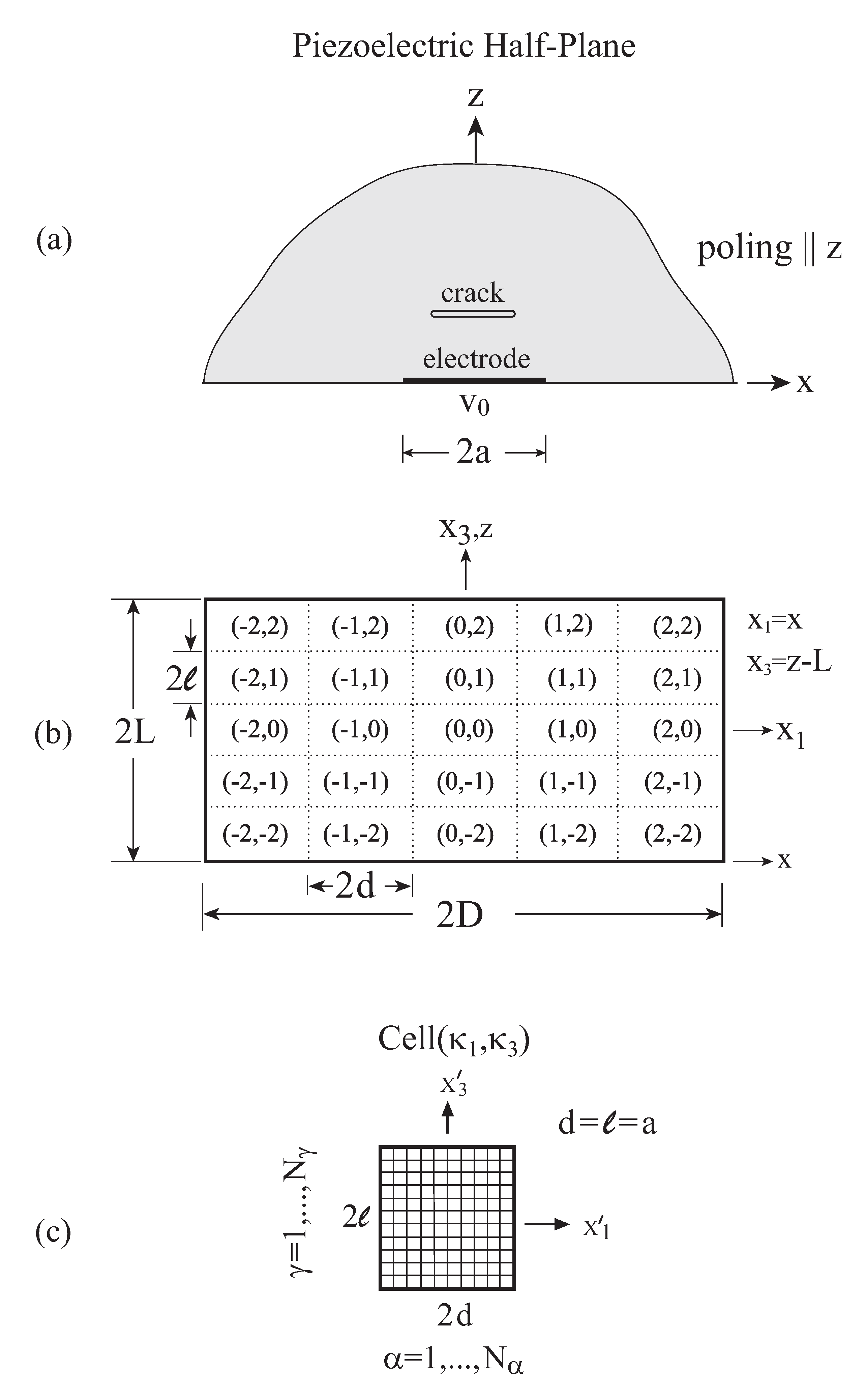
Consider a piezoelectric half-plane
,
z ≥ 0 with an electrode attached to its surface at
z = 0, see
Figure 1a. The poling direction (axis of symmetry) of the piezoelectric material is oriented in the
z-direction, and the electrode extends over
, with its voltage being set equal to
V. As will be discussed in the following, the formulation of the field variables in the piezoelectric half-plane will be carried out in a rectangular region defined by
,
, where
and
; see
Figure 1b.
The constitutive equations of the piezoelectric material are given by
where
and
denote the stress and strain tensors, whereas
and
are the electric displacement and electrical field vectors, respectively. The material properties are specified by the elastic stiffness
, piezoelectric
, and electric permittivity
tensors, respectively. The stiffness tensor
consists of five independent components
, and
,
consists of the three components
, and
, whereas
consists of
and
.
The small strain tensor
is given in terms of the displacement vector
according to the following:
whereas the electrical field
is expressed in terms of the electric potential
according to the following:
In the absence of body forces, the equilibrium equations are given by
and in the absence of volume charges, the following Maxwell’s equation
must be satisfied.
The piezoelectric material that is described by Equation (
1) may characterize a homogeneous material (e.g., PZT ceramic) or a homogenized piezoelectric composite (e.g., PZT/epoxy). In the latter case, the material constants
,
, and
are the effective moduli
,
, and
of the composite which should be determined by employing a suitable micromechanics analysis. In the present investigation, the HFGMC micromechanics analysis in [
14] is employed for the prediction of the effective electroelastic constants of the periodically bilayered composite that will be discussed in one of the present applications. Alternatively, the present analysis can be applied on a piezoelectric composite with distinct phases. In this case, interfacial conditions must be imposed to ensure the continuity of tractions
, mechanical displacements
, electric potentials
, and the normal components of the electric displacements
:
where labels 1 and 2 refer to the two constituents separated between the interface for which normal is
.
The loading conditions at the half-plane surface
z = 0 are given by
Finally, the conditions of vanishing field variables at infinity should be ensured.
The above constitutive relations (Equation (
1)) can be represented in a compact form by defining the vectors
and
as follows:
Consequently, Equation (
1) can be written in the following matrix form:
where the square 9th-order symmetric matrix of coefficients
has the following form:
In Equation (
11),
is the 6th-order stiffness matrix,
denotes the transpose of the rectangular 3 by 6 piezoelectric matrix
, and
is the diagonal permittivity matrix of order 3.
As discussed in the following, the internal defects and the boundary conditions at the surface
z = 0 of the half-plane are simulated by introducing a damage tensor
such that Equation (
10) is modified to
with
. A proper selection of the 10 independent damage components of
enables the modeling of internal defects in the form of cracks, notches, stiff and soft inclusions, and cavities embedded in the material. Furthermore, traction-free boundary conditions
= 0,
j = 1, 2, 3, can be imposed at
z = 0, and
= 0 can be imposed at
of this surface by a suitable choice of the elements of
.
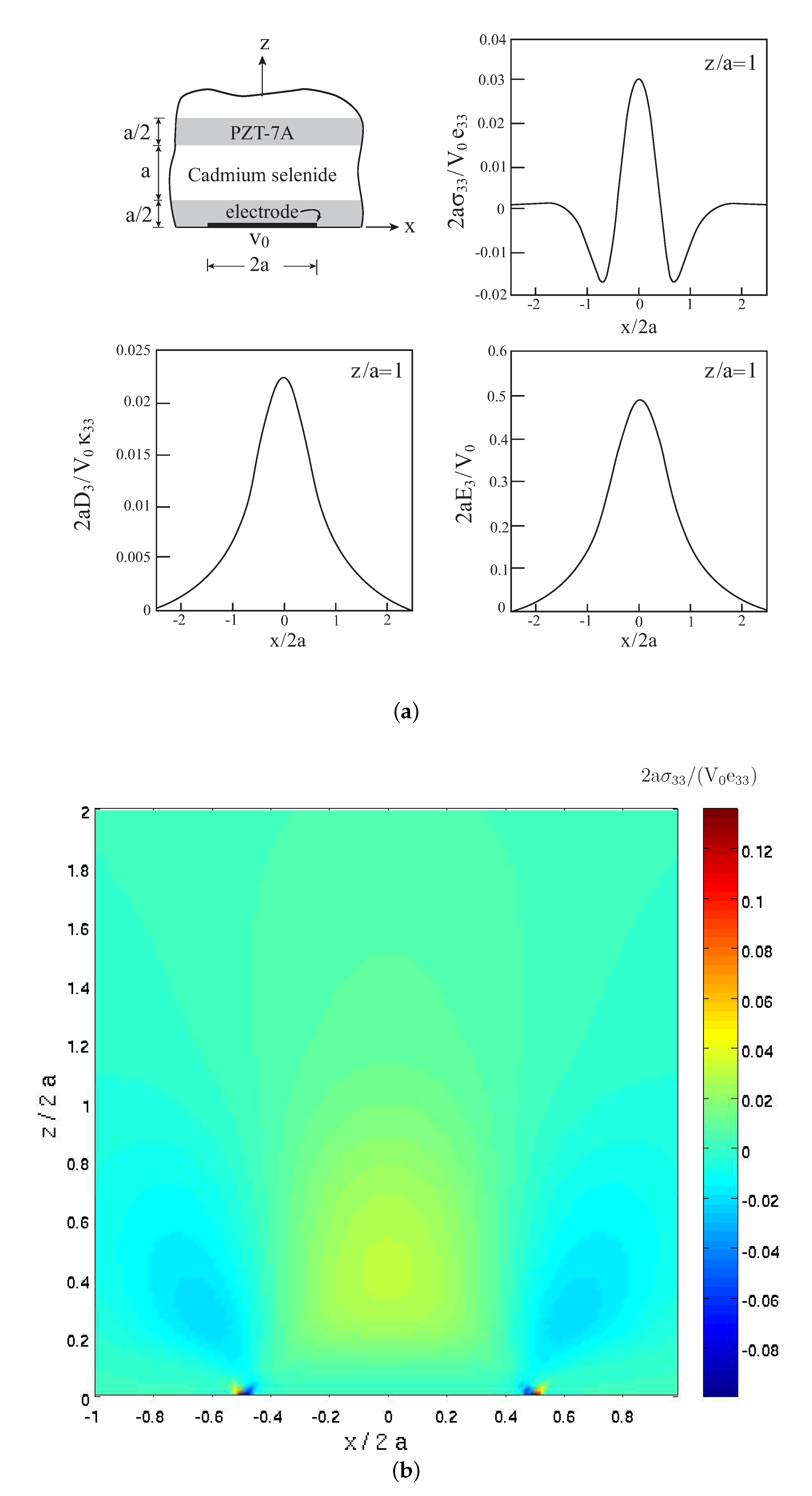
4. Applications
Applications are given for a PZT-7A piezoelectric half-plane with an attached surface electrode which consists of an internal damage in the form of a cavity, a short crack, as well as a long crack. Furthermore, results are shown for a periodically bilayered half-plane with a short crack within one of its layers. The induced mechanical field as well as the resulting electric field are shown in all cases. The material properties of the PZT-7A are given in
Table 1.
All the results shown in the present article have been generated by employing
= 5 and
= 10, namely the rectangular region
,
that has been divided into 11 × 21 cells. The representative cell
,
(
) (
Figure 1c) has been divided in the framework of the higher-order theory into
and
subcells. On the other hand, in the case of the damage in the form of a cavity within the piezoelectric half-plane,
= 100,
= 100 subcells were chosen in order to obtain a good representation of the circular shape.
The computational efficiency of the present approach can be illustrated as follows. The higher-order analysis requires the solution of 32 unknowns in each subcell. Hence, the discretization with 56 × 56 subcells requires for each combination of the harmonic numbers (, ) for the solution of a sparse system of algebraic equations. A direct numerical solution on the other hand with the same number of degrees of freedom would require solving a system of , which is more that 23 million equations (for the half-plane with the cavity, the number of equations is 320,000, against about 74 million equations). It should be further noted that, in contrast to a direct solution, the number of cells and into which the rectangular domain , is discretized does not modify the number of equations (presently 100,352) which forms a significant advantage of the present method of solution.
4.1. Verification of the Offered Analysis
The present analysis is based on the idea that the application of the jumps (Equation (
14)) of the field variables generated in a homogeneous (undamaged) piezoelectric half-plane with a surface electrode at the boundaries of the rectangular region
,
, should generate the correct solution after its discretization into several cells
, the application of the discrete Fourier transform (Equation (
21)), solving the resulting boundary-value problem (Equations (
24)–(
26)) in the transform domain, followed by its inversion (Equation (
28)). This quite demanding procedure forms a mean for the validation of the present analysis by contrasting its prediction with the exact solution based on Equation (
A9).
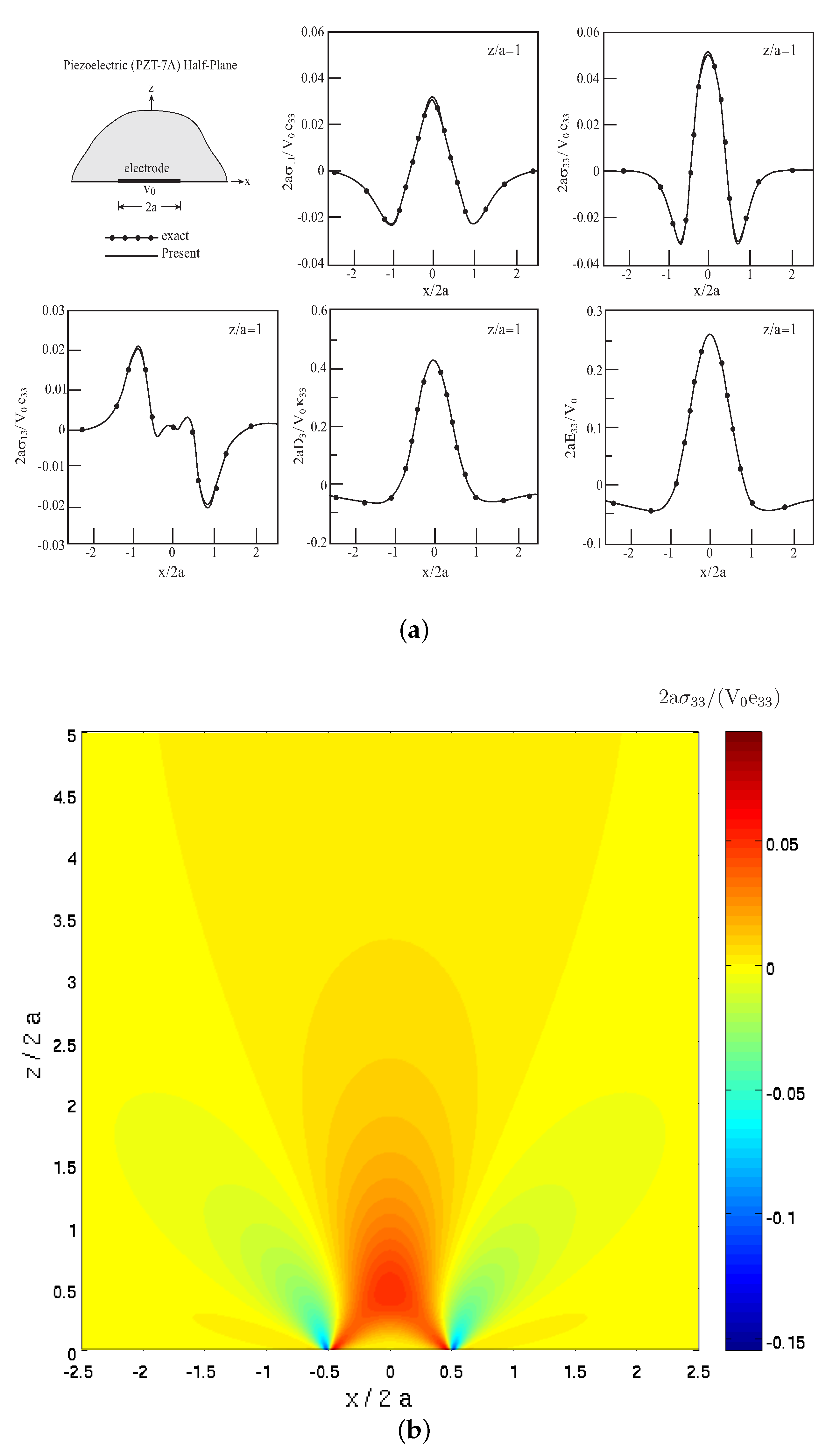
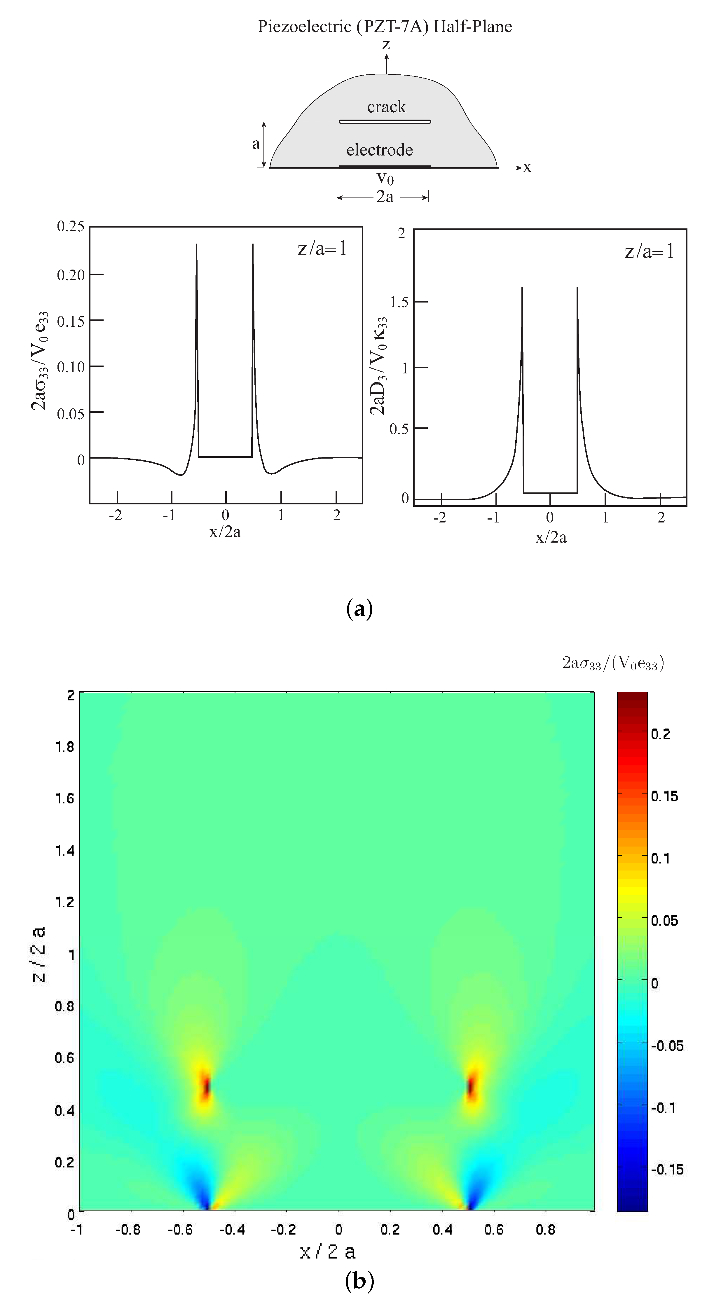
Consider a homogeneous piezoelectric (PZT-7A) half-plane subjected to the loading conditions given by Equation (
7). In
Figure 2a, the variations along the
x-direction at
z/
a = 1 of the normal stress
, shear stresses
and
, normal electric displacement
, and normal electric field component
which are generated by the present approach are contrasted with the exact solution based on Equation (
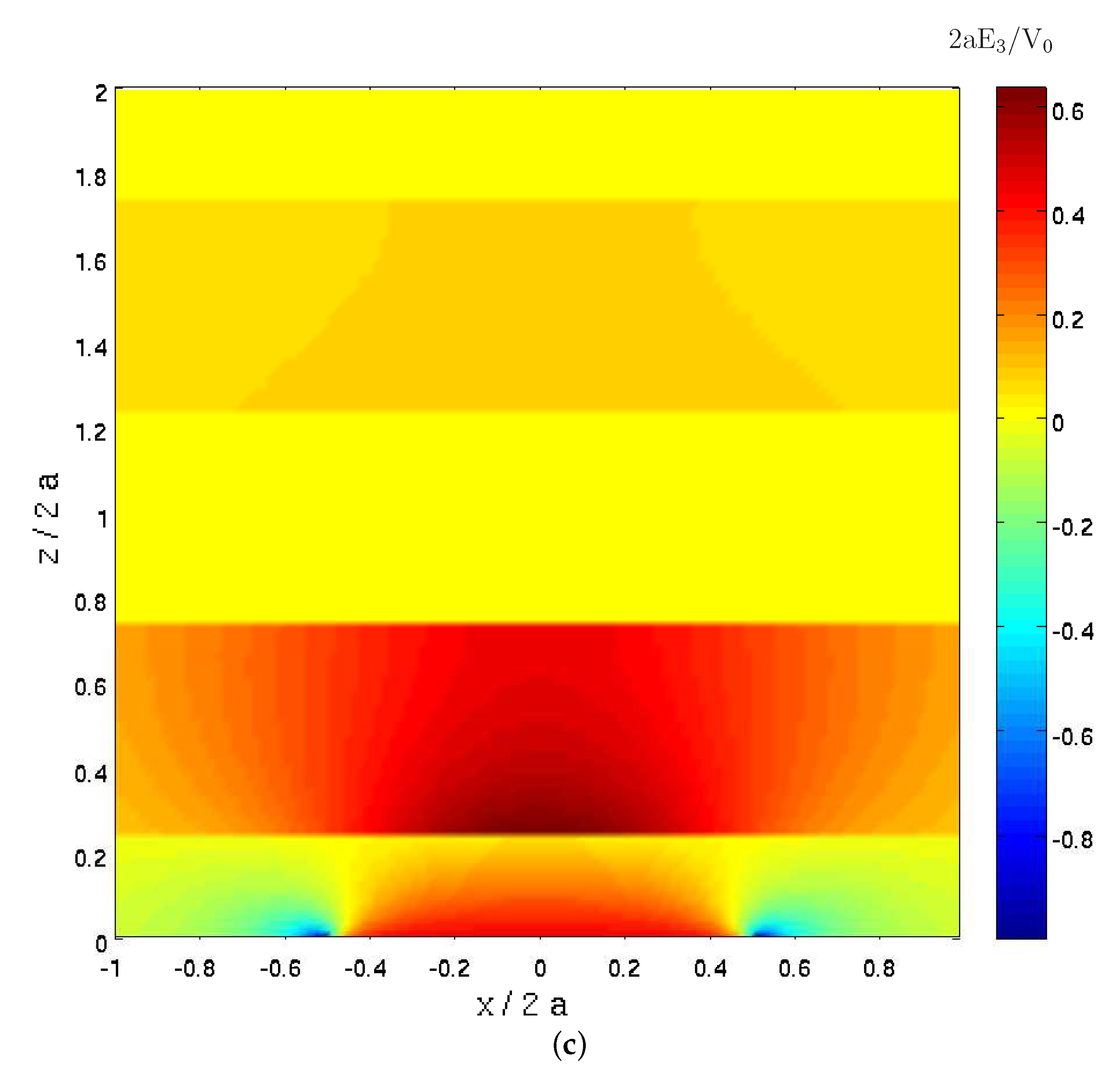
A9). It can be observed that excellent agreements are obtained.
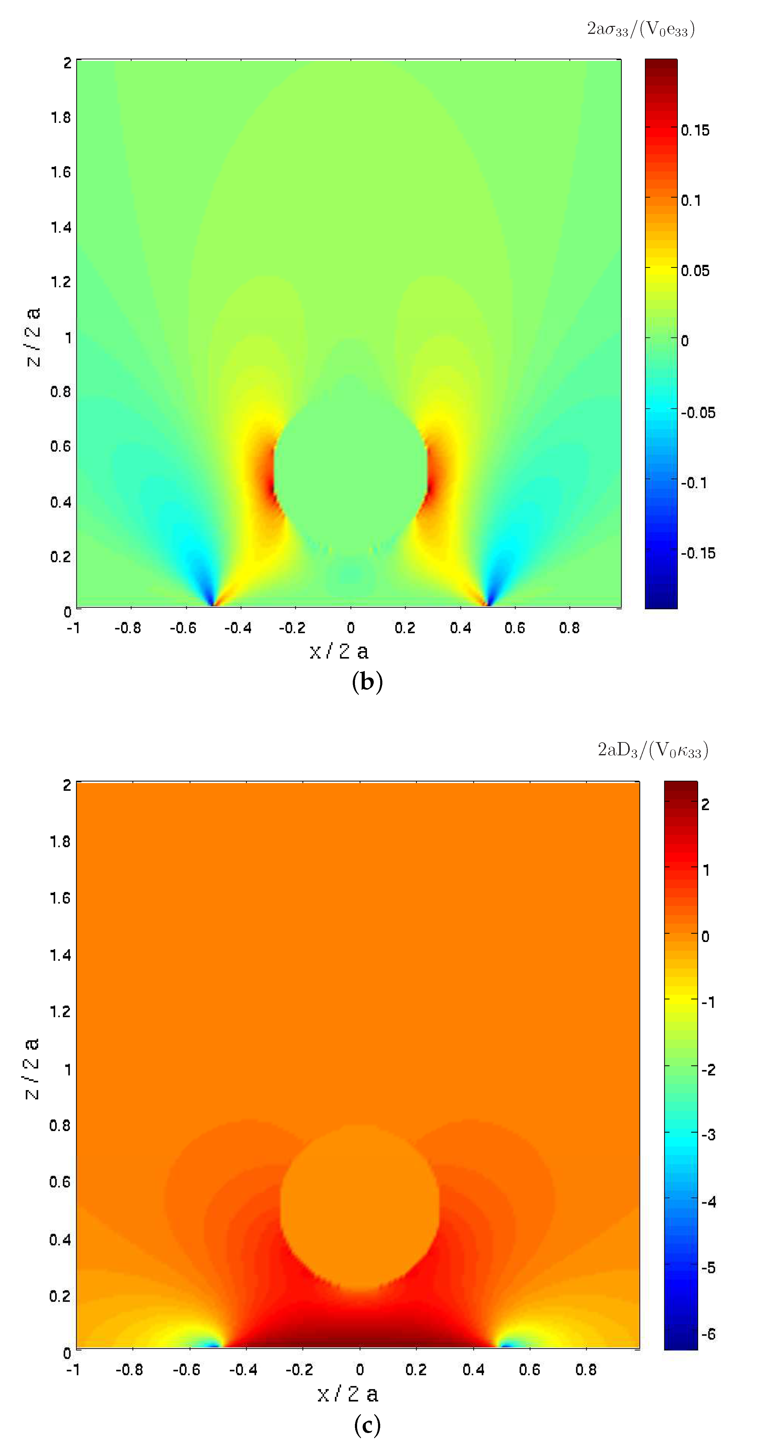
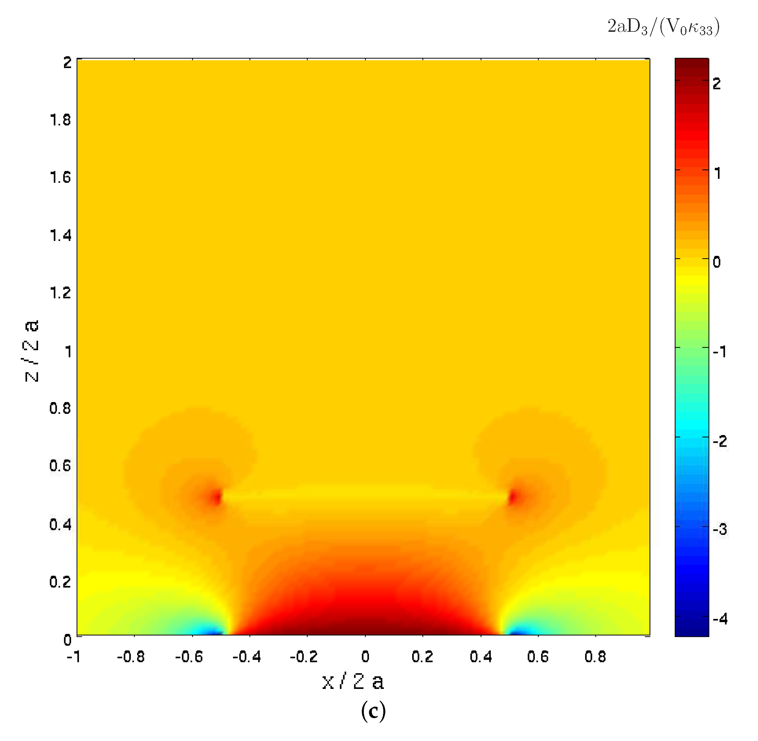
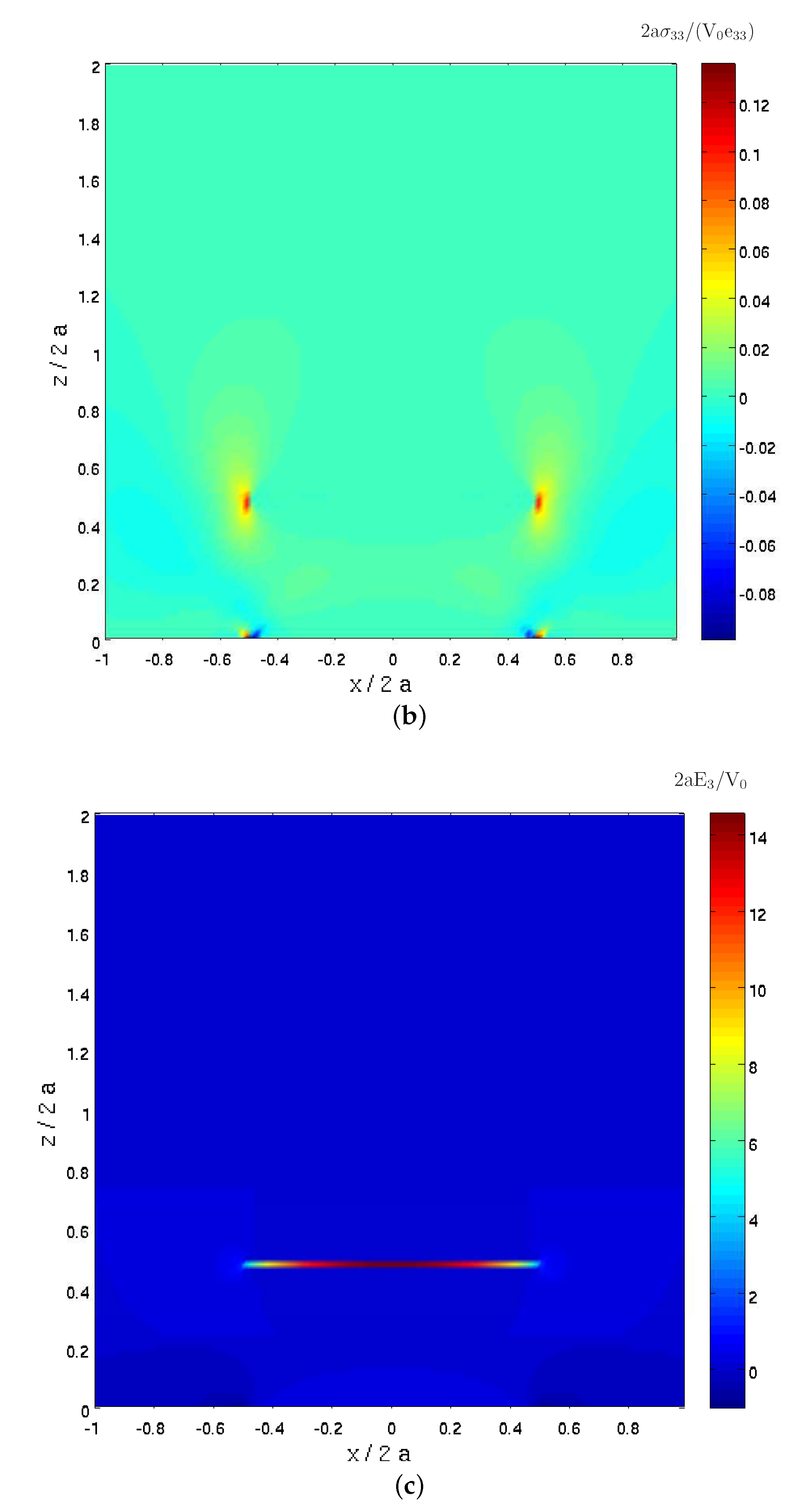
Figure 2b exhibits the distribution of the induced normal stress
in the half-plane in the region
,
as predicted by the present analysis. This distribution can be contrasted with that obtained by the exact solution (
Figure 2c), exhibiting very good correspondence which further validates the offered approach. In
Figure 2d, the distribution of the normal electric displacement
is shown (which is also very similar to the exact one).
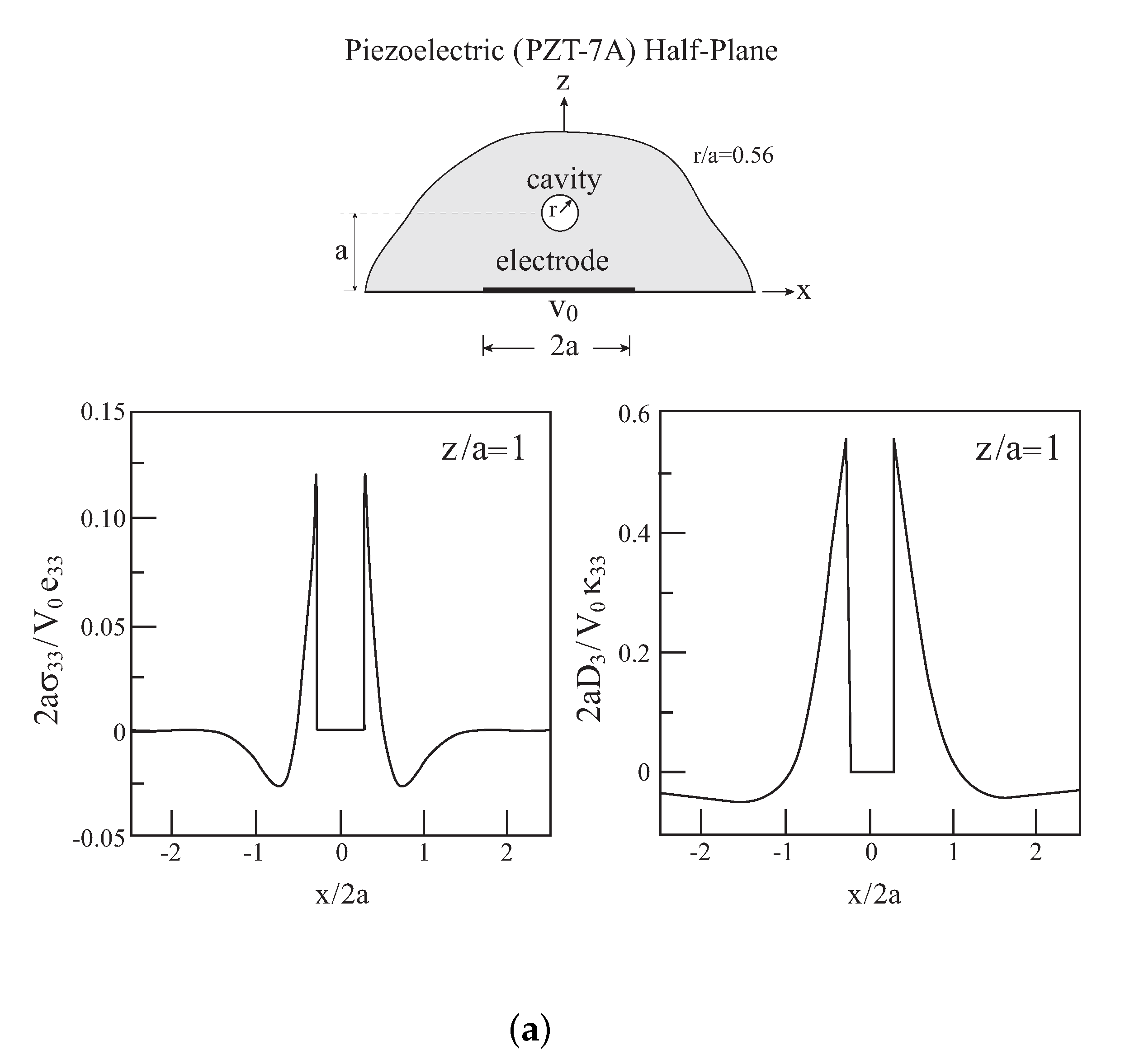
4.2. A Cavity within a Piezoelectric Half-Plane
Consider a defect in the form of a cavity embedded within the piezoelectric (PZT-7A) half-plane with a surface electrode. The radius of the cavity is
r/
a = 0.56, and its center is located at
z/
a = 1 within cell
. As discussed, due to the introduction of this form of damage within the piezoelectric half-plane, it is necessary to activate several damage components of
of Equation (
16). These damage variables should ensure that the traction-free conditions in Equation (
7) at the half-plane surface are satisfied and that the normal component of the electric displacement
there should vanish at
. In addition, the condition of the vanishing field variables within the cavity must be fulfilled. For the traction-free conditions at
z = 0, the damage components of
, which are necessary for the fulfilling the conditions that
= 0,
j = 1, 3, should be set equal to 1 within cells
,
and subcells
,
. For the condition
= 0, on the other hand, cell
= 0 should be excluded. As for the cavity which is located within cell
= 0,
, the damage components of
within the cavity subcells should be set equal to 1.
The resulting induced variations of the normal stress
and electric displacement component
along
z-direction at
z/
a = 1 are shown in
Figure 3a. These plots exhibit both these field variable concentrations at the cavity walls and their vanishing values within the cavity. Furthermore, these variables are clearly observed in
Figure 3b,c in which the distributions of normal stress
and electric displacement
are shown within the half-plane region
,
. A comparison of these figures with the corresponding
Figure 2b,d of the homogeneous case reveals that the presence of the cavity increases the magnitude of the normal stress
, but it has almost no effect on the intensity of the normal electric displacement.
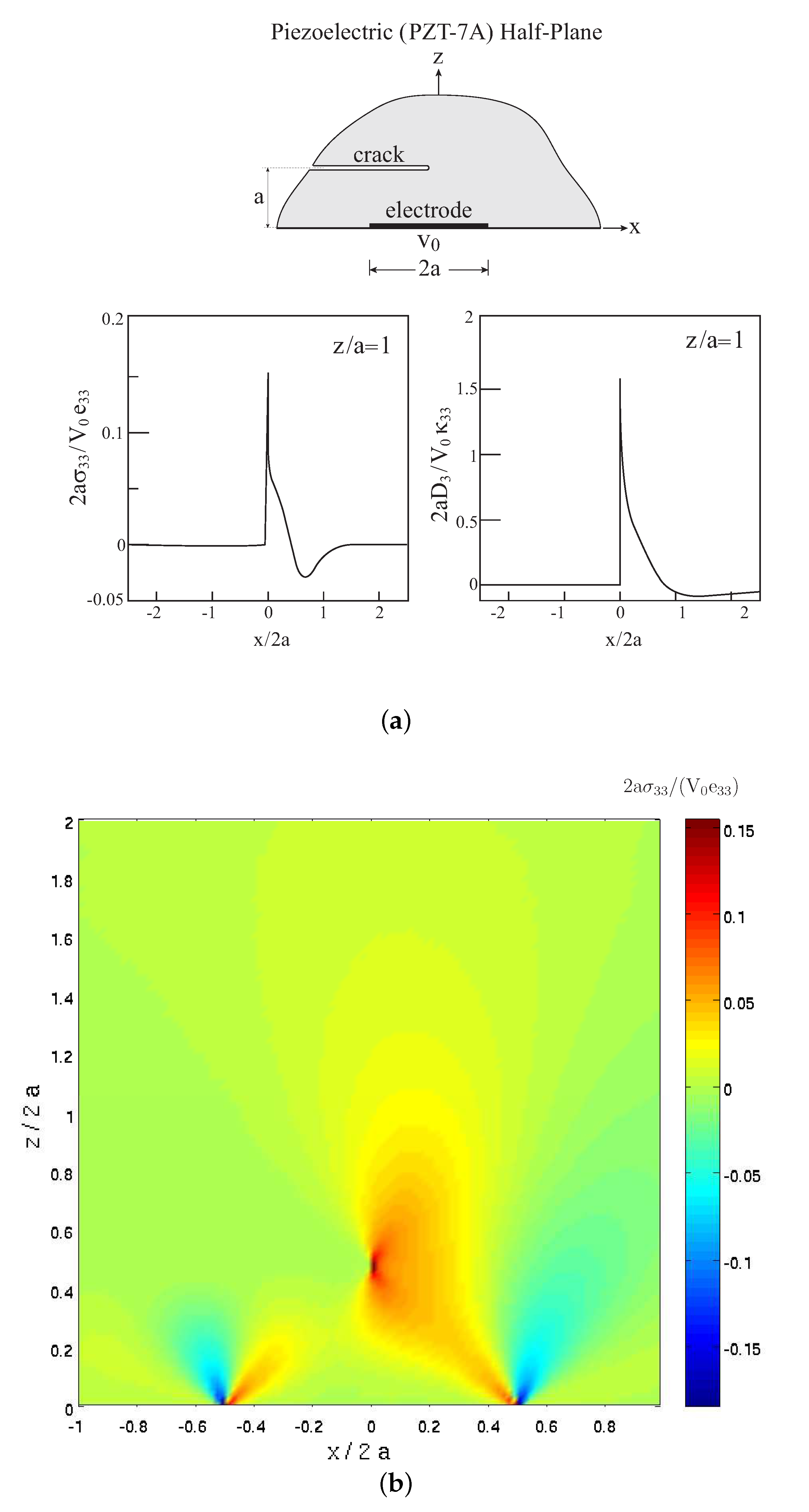
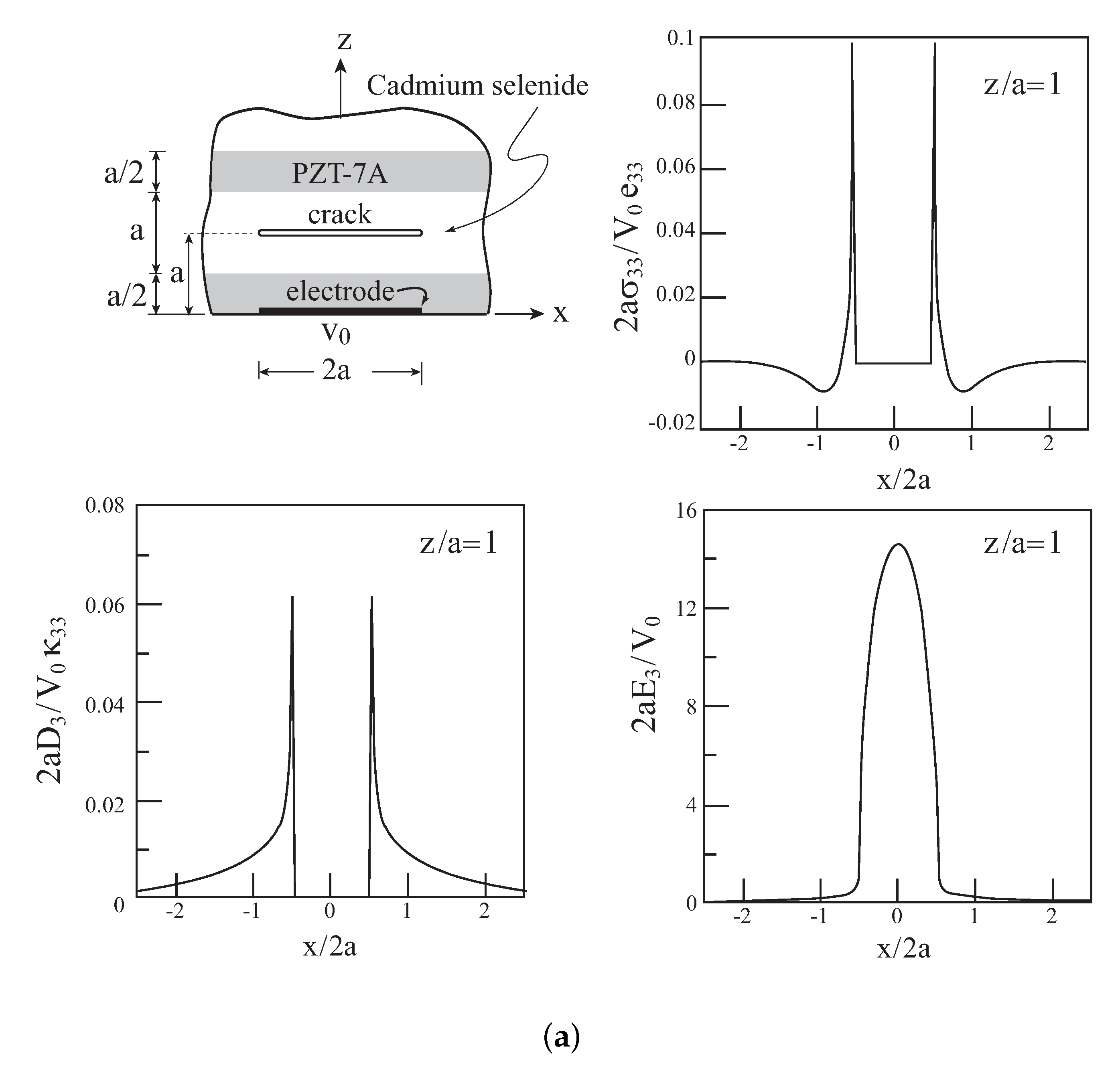
4.3. A Short Crack within a Piezoelectric Half-Plane
The next application discusses the case of a defect in the form of a short crack embedded within the piezoelectric (PZT-7A) half-plane with a surface electrode. The crack is of length 2
a and is located at
z/
a = 1 within cell
and subcells
,
; see
Figure 4a. As in the previous case, the boundary conditions at
z = 0 (Equation (
7)) are similarly imposed here, but along the crack, the appropriate damage variables are set equal to 1 to ensure zero tractions and electric insulation (impermeable crack) along its surface.
Figure 4a exhibits the variations of the induced normal stress
and normal electric displacement
along the crack line at
z/
a = 1. The expected high values of these field variables are clearly shown.
Figure 4b,c shows the full field distributions of
and
. A comparison with
Figure 2b shows the strong shielding effect of the crack on the spread of the stress at the plane. Similar behavior is exhibited by a comparison with
Figure 2d. The effect of the crack on the magnitudes of
and
can be also sought by comparisons of
Figure 4b,c with
Figure 2b,d of the homogeneous case. These show a significant increase of
and a reduction of
.
4.4. A Long Crack within a Piezoelectric Half-Plane
In contrast to the previous case, the considered defect is presently chosen in the form of a semi-infinite (long) crack at
z/
a = 1. The crack is located within cells
,
. For cells
the crack is located within subcells
,
, but within cell
, it extends along
(i.e., the crack terminates at
). As shown in
Figure 2a,
attains its maximum tensile value at
. Thus, it is reasonable to assume that the crack tip is located at this point. Obviously, the appropriate damage variables are set to be equal to 1 along the entire crack locations.
Figure 5a shows the variations of the induced normal stress
and normal electric displacement
along the semi-infinite crack line at
z/
a = 1, whereas
Figure 5b,c show the full field distributions of
and
. These variations and distributions can be contrasted with the corresponding field of the short crack exhibiting significantly different effects between these two cases. The effect of the long crack on the magnitudes of
and
can be observed by comparisons of
Figure 5b,c with
Figure 2b,d of the homogeneous case. Here, a slight increase of the normal stress and a reduction of
can be detected.
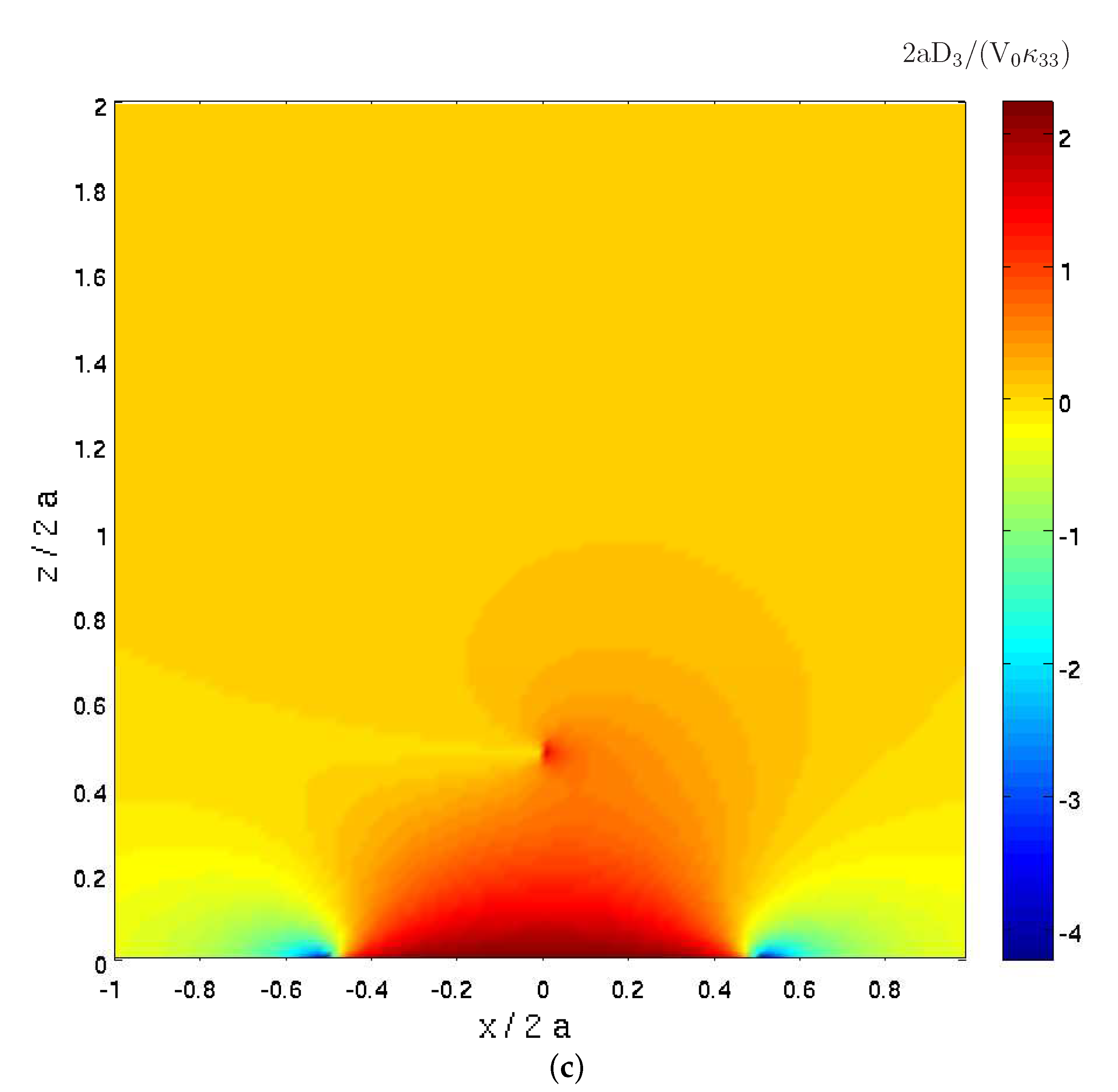
4.5. Piezoelectric Periodically Bilayered Half-Plane
Thus far, a homogeneous piezoelectric (PZT-7A) half-plane with three types of defects has been investigated. Presently, consider a half-plane which consists of piezoelectric layers which are arranged in a periodic manner; see
Figure 6a. Thus, the present case illustrates the analysis of piezoelectric composite half-planes with attached surface electrode in which the composite consists of distinct (unhomogenized) constituents. Since the exact solution of Reference [
2] was derived under the assumption that the poling of the homogeneous piezoelectric half-plane is oriented in the
z-direction, the considered composite periodically bilayered half-plane that is shown in
Figure 6a possesses the correct poling direction since the poling of both layers is oriented in this direction and is identical with the axis of symmetry of the homogenized composite. Thus, the present analysis which uses the solution of Reference [
2] for homogeneous piezoelectric materials is able to model piezoelectric composites with distinct phases as long as the their global poling direction is oriented in the correct direction.
As shown in this figure, the considered bilayered composite consists of a PZT-7A layer to which the electrode is attached at the surface
z = 0, followed by cadmium selenide piezoelectric layer, and so on. The volume ratio
of every constituent is equal to 0.5. The material properties of the cadmium selenide are given in
Table 1, which indicates that this material is characterized by smaller elastic stiffnesses, piezoelectric coefficients, and permittivities. In the present case, the exact solution (Equation (
A9)) must be employed by utilizing the effective properties of the considered piezoelectric periodically bilayered composite. These effective properties have been established by employing the HFGMC micromechanics analysis; see [
14] for details. They are listed in
Table 1. As discussed, the resulting exact field values are employed in Equation (
14) to compute the jumps
and
that are need in the method of solution.
As previously discussed, the tractions-free and the condition on the normal electric displacement at the half-plane surface z = 0 are imposed by selecting the appropriate damage variables in these locations to be equal to unity.
Figure 6a shows the variations of the normal stress
, normal electric displacement
, and normal component of the electric field
along x at
z/
a =1, whereas
Figure 6b,c exhibits the distributions of
and
, respectively, in the region
,
. It should be noted that the normalization of all field variables in these figures are performed with respect to material constants of the PZT-7A layer. The magnitude of
at
z/
a = 1, which is located at the cadmium selenide layer, is about 0.03. A comparison with the homogeneous half-plane that is shown in
Figure 2 reveals that the corespondent magnitude is 0.05. Thus, the cadmium selenide layer, which possesses smaller elastic stifnesses as compared to the PZT layer, suppresses the induced normal stress. A similar observation concerns the electrical normal displacement
. A comparison of maximum of
variation in the cadmium selenide layer in
Figure 6a with the variation shown in
Figure 2a reveals about 20 times decrease of this field variable within this layer.
In order to distinguish between the different layers of the composite,
Figure 6c shows the distribution of the normal component of the electric field
because this component is not continuous across the layers. This is in contrast to the distributions of
and
which are continuous across the layers and therefore cannot distinguish between the layers.
In conclusion, the present application illustrates the ability of the present method to analyze piezoelectric composite half-planes with surface electrode by utilizing the exact solution of Reference [
2] (Equation (
A9)) of homogeneous piezoelectric half-planes. The composite half-planes are composed of distinct constituents, but the axis of symmetry of the homogenized composite half-plane must be oriented in the
z-direction.
4.6. Cracked Piezoelectric Periodically Bilayered Half-Plane
In the previous application, the present analysis has been applied to predict the behavior of periodically bilayered PZT-7A/cadmium selenide half-plane. As discussed, defects in the composite half-planes can be introduced by a proper selection of the damage variables in the damaged locations. In the present application, the periodically bilayered PZT-7A/cadmium selenide composite half-plane is considered but with the introduction of a defect in the form of a short crack of length 2
a embedded within the mechanically soft cadmium selenide layer at
z = a; see
Figure 7a. This crack is located within cell
and subcells
,
.
Figure 7a shows the variations of
,
, and
along the crack line at
z/
a = 1. The expected high values of the normal stress and normal electric displacement at the vicinity of the crack tip are clearly exhibited. A comparison with the corresponding variations of the cracked homogeneous half-plane (
Figure 4a) shows that the both
and
attain lower values in the present layered case, indicating the suppressing effect of the cadmium selenide layer. This can be also observed by comparing the resulting stress distribution in the layered half-plane in
Figure 7b with the distribution of
Figure 4b of the homogeneous case. Finally,
Figure 7c shows the distribution of the normal component of the electric field
. Due to the resulting high values that are caused by the crack (the maximum values of
≈ 0.5 and 15 at
z/
a = 1 in the uncracked and cracked cases, respectively), it is presently almost impossible to distinguish between the layers.
5. Conclusions
A method for the prediction of the behavior of piezoelectric composite half-planes with attached surface electrode is presented. The composite half-planes are composed of distinct constituents, and their behavior is determined in conjunction with the closed-form expressions of the corresponding homogenized piezoelectric half-plane in which the electromechanical constants are determined by a micromechanical analysis. Furthermore, the offered method is capable of predicting the effect of localized damages on the electromechanical field in the considered piezoelectric composite half-planes.
The present analysis is based on the combined application of HFGMC micromechanical model (which predicts the effective constants of the composite), the representative cell method (according to which a rectangular region is divided into numerous cells), the higher-order theory (which solves the resulting boundary-value problem in the discrete Fourier transform domain), followed by the inversion of the transform to obtain the field variables at any point of the region. The imposed boundary conditions are based on the exact solution of Reference [
2] for homogeneous piezoelectric half-plane. Damage variables are introduced to ensure the fulfillment of the half-plane boundary conditions and to model the chosen forms of the defects. Verification of the method has been performed by examining the ability of the offered method to recover the exact solution. The method has been illustrated for defects in the form of single cavity and short and semi-infinite cracks in a piezoelectric half-plane with surface electrode. In addition, the method has been applied for the prediction of periodically bilayered half-plane composite with and without defect. For simplicity, single defects in the form of a cavity or crack have been considered, but the method can be applied on piezoelectric half-plane composites with multiple internal defects.
In the absence of damage, the analysis in the present article provides a mean to detect the microstructure and field distributions of the piezoelectric composite. This is performed by considering a piezoelectric composite half-plane on the surface of which an electrode has been applied. The resulting structure of the distinct constituents in the composite and of the electromechanical field distribution can be readily obtained. This procedure has been illustrated in
Figure 6, where a composite half-plane that consists of doubly periodic layers of different piezoelectric materials has been considered. Next, in the presence of damage in the piezoelectric composite, the present analysis is capable of generating the electromechanical field in the half-plane which is loaded by the electrode. This field distribution exhibits the locations where high high stresses and electric fields exist. This procedure has been illustrated in the presence of damage in the form of a cavity and of short and long cracks. It is obvious that other types of damage can be considered. Clearly, this information is useful in the design of piezoelectric composites in which defects may exist due to faulty manufacturing or during service and for understanding their failure. Briefly saying, the present analysis offers a theoretical sensor for the study of the microstructure and field distribution in piezoelectric composites in the absence and presence of damage.
The present approach can be employed for the prediction of the electromechanical effects caused by electrodes located at the interface between two piezoelectric composite half-planes with internal defects. The necessary boundary conditions to be imposed in these investigations may utilize the analytical expressions of References [
18,
19,
20], for example. The offered method can be further generalized for piezoelectric composite half-planes that are subjected to combined electromechanical surface loadings. For a piezoelectric homogeneous half-plane under a combined surface loading, see Reference [
21], for example.


