1. Introduction
In recent years, additive manufacturing (AM) has emerged as a transformative technology with profound implications across various industries, including aerospace, healthcare, automotive, and beyond [
1]. The unique capabilities of AM—particularly in terms of material diversity, precision, and design freedom—have opened the way for novel applications in the field of communication systems. The communications industry increasingly demands higher frequency devices capable of handling the complex requirements of modern wireless systems [
2]. Additive manufacturing offers several advantages in meeting these demands. First, it enables rapid prototyping and iterative testing, allowing engineers to optimize designs in shorter time frames [
3]. This rapid design-to-manufacture process is essential for the fast-paced communications sector, where technologies are continuously evolving to support new standards like 5G and 6G [
4]. Secondly, AM facilitates the production of highly intricate structures that are difficult to machine or mold. For example, horn antennas and GRIN lenses with complex internal geometries can be manufactured as single components, reducing the need for assembly and the potential for alignment errors, which are critical factors in RF applications [
5].
Antenna design has evolved significantly in response to the ever-growing demand for high-performance communication systems. Traditionally, antennas are fabricated from metals such as copper or aluminum, chosen for their high electrical conductivity and robustness in high-frequency applications. The horn antenna, a staple in RF communications, is particularly valued for its simplicity, directivity, and broadband capabilities [
6]. With the advent of AM, researchers have explored new methods to manufacture these antennas, often focusing on materials and processes that allow for high precision and reduced weight. Metallic coatings can be applied to 3D-printed polymer structures to achieve the necessary conductivity [
7]. Shen et al. [
8] offers a more versatile manufacturing process for complex designs. This approach not only reduces the weight of the component but also lowers material costs by limiting the use of expensive metals to surface coatings, customizing antenna properties without the constraints of conventional subtractive manufacturing. By enabling the use of composite polymer-based materials, AM also enhances the thermal management of devices, which is especially important for high-power applications in the communications field [
9].
Gradient Index (GRIN) lenses are widely used in communications to manipulate the propagation of electromagnetic waves. By gradually varying the refractive index of the lens material, GRIN lenses focus or direct RF energy in a controlled manner, enhancing the performance of antennas in terms of gain and beam shaping [
10]. Traditionally, these lenses are made from homogenous dielectric materials, with their refractive index modified by altering their geometry [
11]. This often requires a labor-intensive shaping of dielectric materials to achieve the desired index gradient, which limits design flexibility and increases production time. However, AM provides the ability to adjust the refractive index more flexibly by changing the density or porosity of the polymeric material within a single component during fabrication. This method also allows for the integration of stochastic and gyroid mesh structures, which offers an additional degree of control over material properties. By adjusting the porosity of the material, designers can achieve specific permittivity values across the lens profile, as in [
12,
13]. This capability opens up new possibilities in lens design, enabling devices that are both lightweight and capable of complex wavefront shaping.
There are several AM techniques that are particularly suited to the polymer-based fabrication of RF components, for instance, Vat Photopolymerization (VPP) and Powder Bed Fusion (PBF). VPP, which uses ultraviolet light to selectively cure photopolymer resins, is valued for its high resolution and is often used to fabricate intricate components such as waveguides and lenses. In contrast, PBF enables the use of materials like polyamide polymer, which is lightweight and offers good mechanical stability and electrical transparency. As detailed by [
14], using PBF to create support structures in RF devices enables engineers to maintain both structural integrity and desired electromagnetic transparency. The integration of these AM techniques has driven substantial advancements in the manufacture of complex antenna and lens structures, especially when complemented with material innovations like electroless metallization [
15,
16,
17].
This article outlines the research gap that existed between integration of different additive manufacturing techniques (VPP, PBF), electroless metallization, and used materials (resin or nylon polymer) in developing radio frequency (RF) communication devices (previous measurements of EM properties of the material samples are accomplished in
Section 2.2.4. Specifically, it focuses on the development of a horn antenna and a Gradient Index (GRIN) lens set, designed for operation in the X-band frequency range, making use of the capabilities of AM of polymeric materials. The work begins with measuring the dielectric permittivity and loss tangent of different polymeric materials at frequencies of 2.45 (WiFi at 2.4 GHz, 3G/4G mobile bands), 6.25 (WiFi at 5 GHz, 5G mobile bands, satellite communications), and 24.5 GHz (6G mobile bands, satellite communications). Furthermore, samples of stochastic and gyroid mesh structures of the different materials were measured, and the empirical relationships between material density and electromagnetic properties were established.
Then, the lens set was designed. The design of the horn antenna, lens, and support structure was tailored to their specific functional requirements, both electromagnetic and mechanical. Three realizations of the GRIN lens were produced, using the results of the characterization of polymers whose dielectric properties vary with density, allowing for a radial permittivity gradient that enhances its focusing capabilities.
The sets were then manufactured. The horn antenna, designed to be conductive, was fabricated using VPP with an acrylic resin with silica load and subsequently metallized using an electroless plating process. This combination ensures that the antenna meets the necessary conductivity specifications while benefiting from the lightweight and cost-effective nature of the polymer base. The support structure was fabricated using PBF with polyamide polymer, chosen for its mechanical stability and electrical transparency. This allows the support to maintain the structural integrity of the device without interfering with the antenna’s radiation pattern. Finally, the three GRIN lenses were manufactured using different acrylic resins and meshes with different densities radially distributed.
The final assembled devices were then evaluated for frequency response and radiation pattern, yielding results that aligned well with theoretical predictions and those of comparable studies in the existing literature.
2. Dielectric Permittivity Measurements
A material that can store energy when an external electric field is applied is known as a dielectric. Since the advent of modern communications, dielectric materials have been included in antennas and RF components; thus, the accurate measurement of their properties is crucial. The main parameter of dielectric properties is permittivity
and is expressed as in Equation (
1) where
is called the permittivity of vacuum and
is the relative permittivity of the material.
where the permittivity of vacuum is
F/m. The relative permittivity
is a complex number including the real part
, which shows how much energy from an external electric field is stored. Usually, the term dielectric constant relates only to this real part, while the imaginary part
represents how dissipative or lossy this material is to an external electric field. The ratio of the energy lost to the energy stored is called the loss tangent or
, see Equation (
2).
The characterization of these two parameters in new materials is essential for the proper design of devices that make use of them.
2.1. Microwave Characterization Methods
Methods for characterizing the samples can be divided into non-resonant and resonant categories. In non-resonant methods, material properties are determined using reflection or reflection/transmission data in a transmission line. This data is collected via a vector network analyzer (VNA) in a wide frequency range. Transmission/reflection methods require both reflection and transmission data (scattering parameters and , respectively) to determine material properties, whereas reflection methods only need reflection data (). Various transmission lines, including coaxial lines, hollow metallic waveguides, dielectric waveguides, and free space, can be utilized in these methods.
Resonant methods offer greater accuracy and sensitivity compared to non-resonant methods [
18], but they are restricted to one or a few discrete frequencies. These methods are divided into the methods of material under test (MUT) as a resonator and the resonant perturbation methods. The main difference between them is that in the resonant perturbation method, the properties of the MUT are determined by observing changes in the properties of a resonant device with and without the MUT, whereas the MUT as a resonator method relies directly on how an MUT behaves as a resonator with its resonant properties. In resonant methods, the dimensions of the MUT are crucial since they impact the measurement, so accurate dimensional control is required.
Three measurement methods were used in this work to characterize the AM polymeric material samples at a narrow band; all of them are considered resonant perturbation methods: Resonant Coaxial Bireentrant Microwave Cavity at 2.45 GHz, Split-Cylinder Resonant Cavity at 6.25 GHz, and Rectangular Waveguide at 24.5 GHz.
2.1.1. Resonant Coaxial Bireentrant Microwave Cavity
In the method described in [
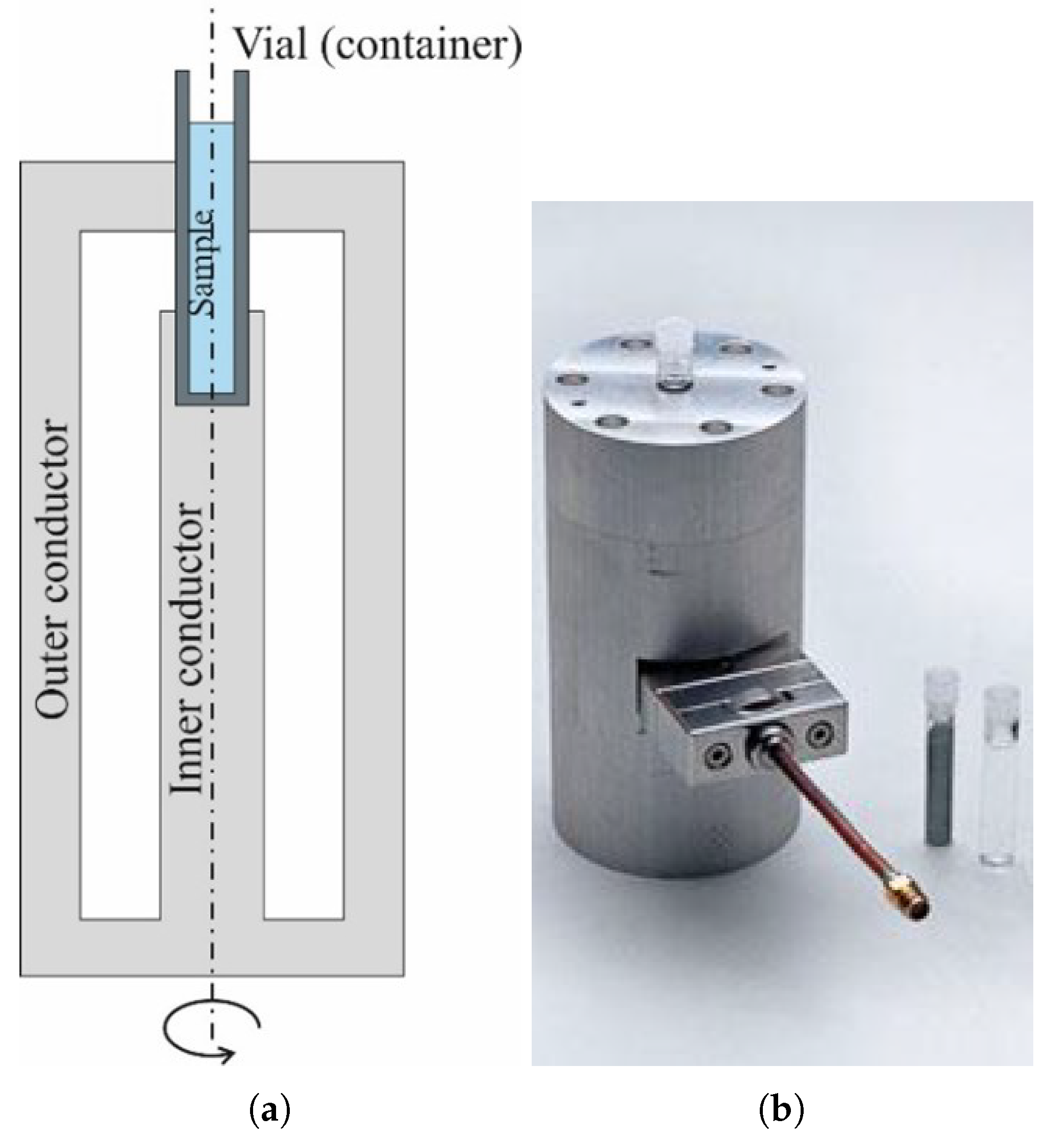
19], the measurements are based on how the resonant frequency and the quality factor of a resonant cavity change when a cylindrical sample of MUT is introduced into the cavity. The Single-post coaxial reentrant cavity is constructed using a coaxial transmission line, where a rod sample is introduced in a gap created in the inner conductor,
Figure 1a. This cavity features a partially dielectric-filled gap and an endplate. To ensure alignment, a cylindrical tube housing the cylindrical sample of MUT is inserted through a hole in the endplate, see
Figure 1b. It is then further inserted into the coaxial center conductor, which also serves to maintain concentricity. In order to perform the measurements a stand-alone microwave equipment, Dielectric Kit for Vials (DKV) from the Institute of Information and Communication Technologies (ITACA) settled in Valencia, Spain, which consisted of a Single-Post Reentrant Cavity for measuring cylindrical samples at resonance frequency of 2.45 GHz (mode
is excited in the cavity without sample), as shown in
Figure 2a, and a VNA are used. Measuring the reflection coefficient (
) of the cavity with and without the sample enables the extraction of the dielectric constant and the loss tangent. The procedure is described in detail at [
20], where the circuital analysis of dielectric-loaded cylindrical waveguides and cavities is performed. The measurement equipment is detailed in [
21].
2.1.2. Split-Cylinder Resonant Cavity
The split-cylinder resonator is a nondestructive technique used to measure the permittivity and loss tangent of low-loss dielectric substrates. Initially proposed by Kent [
22], this method utilizes a circular-cylindrical cavity divided into two halves. A planar dielectric sample is positioned in the gap between the two shorted cylindrical waveguide sections. To excite the family of resonant modes, coupling loops in the cylindrical waveguide sections are connected to the input ports of a network analyzer. By measuring the resonant frequency (
) and quality factor (Q) of the
resonant modes, the relative permittivity and loss tangent of the sample can be determined. This procedure is based on an analytical model first developed by Michael D. Janezic and James Baker-Jarvis [
23,
24].
The equipment used is a Split-Cylinder Cavity, from the Institute of Information and Communication Technologies (ITACA) settled in Valencia, Spain, for measuring rectangular flat samples with a resonance frequency of 6.25 GHz (mode
is excited in the cavity at vacuum) and a VNA, as shown in
Figure 2b. Then, MATLAB R2025a software was used to calculate the permittivity of the materials following the circuit analysis described in [
20], with an extension of the circuital model for the circular modes in the split cavity, which can be found in [
25].
2.1.3. Rectangular Waveguide
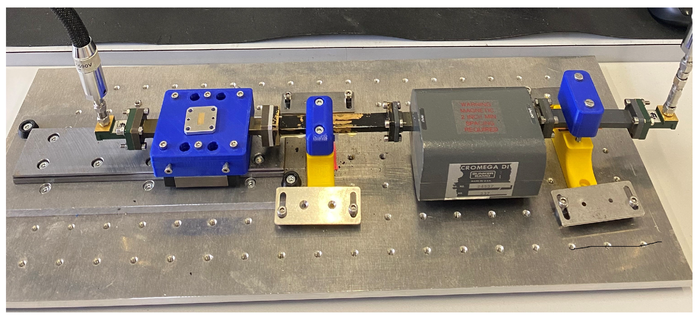
Rectangular waveguide is one of the most commonly used instruments for the measurement of dielectric properties [
26,
27]. A rectangular sample of MUT, with a specified length, is placed in an empty waveguide, provoking a perturbation of an electric field, which is frequency-dependent. By measuring the resulting
and
parameters, the dielectric properties of the MUT at a given frequency can be extracted. For the measurements of the work, the WR42 (18–26.5 GHz) rectangular waveguide is used jointly with a VNA, as shown in
Figure 3. The MUT size must fit the X-band rectangular waveguide aperture, which is 10.668 × 4.318 mm (corresponding to WR42 rectangular waveguide size standard). This measurement setup was used for the MUT characterization at 24.5 GHz.
2.2. Materials
2.2.1. Polymers for Additive Manufacturing
Traditional materials for AM, as PLA or ABS polymers used with FDM technologies, have been characterized at microwave frequencies, and their dielectric constant and tangent loss are well known [
28,
29]. Nevertheless, the advent of new technologies and materials raises the need for analysing their dielectric properties. In this work, six different polymers were characterized: Thought 200 and Rigid 10K resins from Formlabs, MLSA Modelling Dental resin from ApplyLabWork, Composite X (CX) resin from Liqcreate, Ultrasint PP (UPP) powder from BASF, and Polyamide 11 (PA11) Bio powder from Stratasys. Dental and Thought 200 are acrylic resins used by VPP, similar to Rigid 10K and Composite X. However, these last two resins have a load of silica, making them more resistant to temperature, harder, and less prone to deformations. UPP is a polypropylene powder used for Multijet PBF technology, while PA11 is a polyamide powder used in PBF technology.
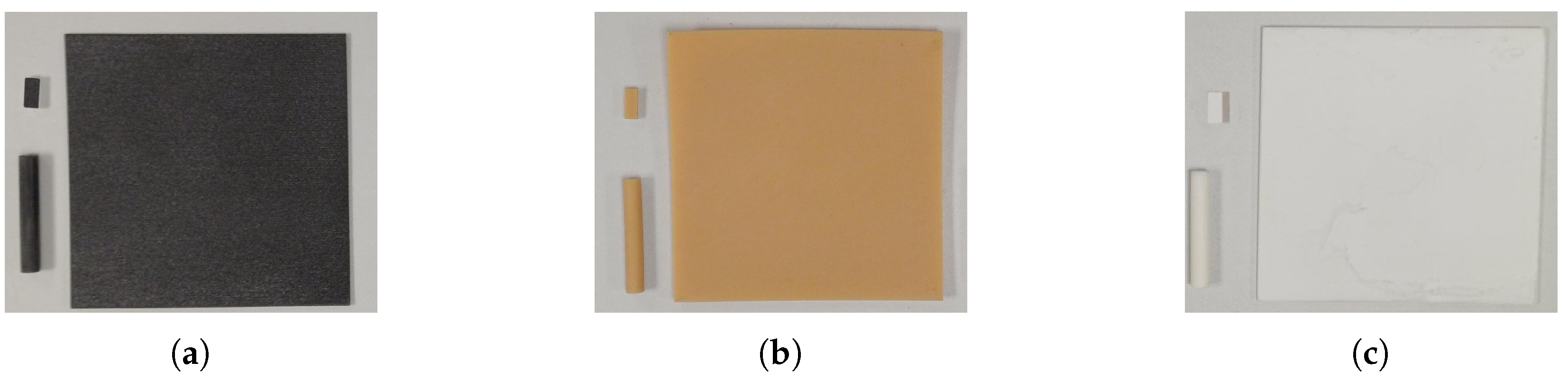
Three different types of samples were printed in order to obtain the measurements at the three frequencies: a cylinder of 6.50 mm of radius and 40 mm of height for the Resonant Coaxial Bireentrant Microwave Cavity at 2.45 GHz, a flat square size 95 × 95 × 2 mm for the Split-Cylinder Resonant Cavity at 6.25 GHz and a cuboid size 10.668 × 4.318 mm and 3 mm of length for the WR42 Rectangular Waveguide at 24.5 GHz, as can be seen in
Figure 4. It should be emphasized that it is not required for the cuboid sample to have precise micron-level dimensions to be measured using the WR42 Rectangular Measurement Kit; it only needs to fit within the waveguide. The small deviations can be corrected with the measurement method used. To design the three geometries, Solidworks software was used.
2.2.2. Permittivity Measurements of Solid Polymers
Table 1 shows the dielectric properties of the different polymers for the three frequencies. The materials show very slight differences in frequency, indicating that within the microwave bandwidth, the dielectric properties are stable. As expected, materials containing silica in the resin (Rigid 10K and Composite X) present a higher dielectric constant, and materials made from polymer powder (UPP and PA11) present a lower one. The same behavior is observed in the material density, which, in the end, will be translated to the weight of the final printed item.
2.2.3. Stochastic and Regular Meshing
Once the solid polymers were characterized, the complex permittivity of the same materials but with different densities was measured. The objective was to have graphs for different materials and frequencies relating density to dielectric properties. Since these properties seem to be quite constant in the frequency range, only the measurements for 2.45 and 24.5 GHz were performed. Furthermore, not all the materials were measured at this stage; since Dental and Though 200 seem to have similar properties, only Dental was used. Composite X and Rigid 10K presented different dielectric constants, so both were measured. Similarly, the measurements were also performed for PA11 and UPP.
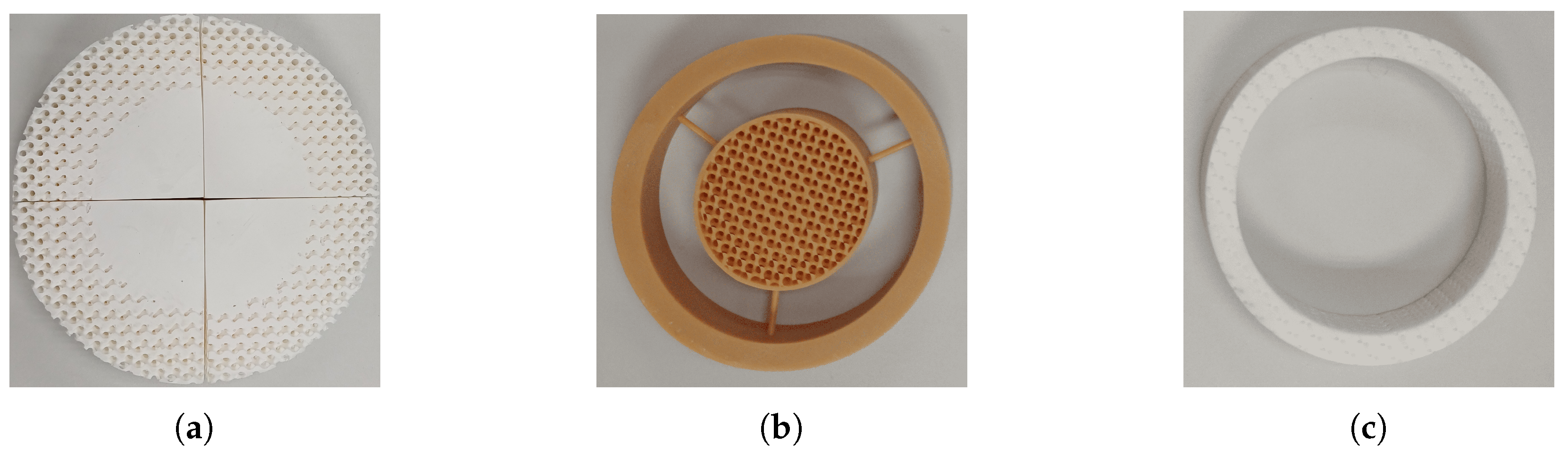
The samples (cylinder and cuboid) were manufactured using porous lattices. These structures are widely used in various fields, including materials science and engineering. They can be broadly categorized into two types, both used in this work: regular lattices (gyroid mesh) and stochastic lattices (Voronoi mesh). The printing densities were 25, 50 and 75% (100% is the solid sample), as it is shown in
Figure 5. To design the gyroid mesh, the Flattpack v.2025 software was used, which is a freely distributed library implemented in Matlab, developed within the framework of the University of Nottingham, and allows for the processing of geometrical objects by directly uploading the models to the program and processing them to obtain porous structures. To design the Voronoi mesh, the Grasshopper 3D tool from Rhinoceros 3D version 8 commercial CAD software was used.
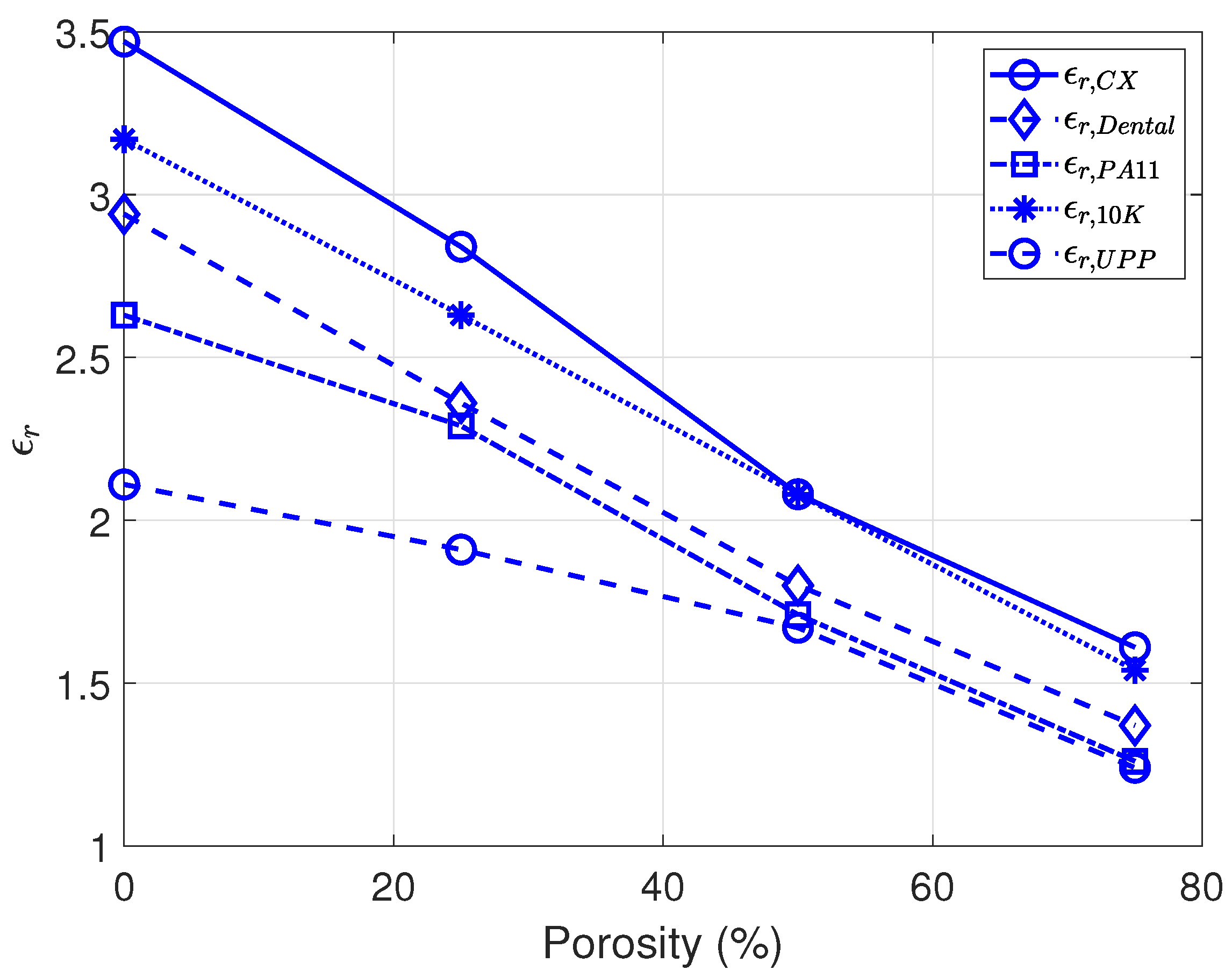
2.2.4. Permittivity Measurements of Porous Polymers
Regarding the porous samples,
Table 2 shows the results for the materials at the two extreme frequencies. The samples were manufactured with gyroid or Voronoi meshes. From these data, the graphs in
Figure 6 and
Figure 7 were extracted, enabling a wide range of permittivities within the same material (at 2.45 and 24.5 GHz, respectively).
Measuring the dielectric properties at 24.5 GHz presents a technological challenge, as methods such as the bi-reentrant cavity and split cylinder do not provide reliable results due to the small size of the samples and cavities and the manufacturing tolerances, so the rectangular waveguide method is used instead. Although this method is reliable for characterizing the dielectric constant, its uncertainty in calculating the loss tangent presents challenges, as stated in [
30,
31], so that the results of the loss tangent at that frequency are missing in this study. However, this uncertainty does not affect the phase, only the attenuation, so the impact of losses is limited to a reduction in gain and radiation efficiency of the antenna set.
3. Horn Antenna and Gradient Index Lens Design
The objective of the design was to obtain a complete set with a horn antenna and GRIN lens, which meet certain EM and mechanical specifications. The main idea behind the GRIN lens is that it focuses the radiation pattern of a radiating element, enhancing the directivity of the set. In this general approach, two main elements were designed, on the one hand, the radiating element, and on the other hand, the lens. The electromagnetic design is frequency-dependant, but scalable, allowing a design developed for one frequency to be easily adjusted for another. The selected working frequency for the set was 10 GHz, covering services in X-band satellite communications. On the other hand, mechanical issues were considered, such as the weight of the set and how the radiation element and the lens are built up together, in order to obtain a compact element ready to be used.
3.1. Electromagnetic Design
3.1.1. Horn Antenna
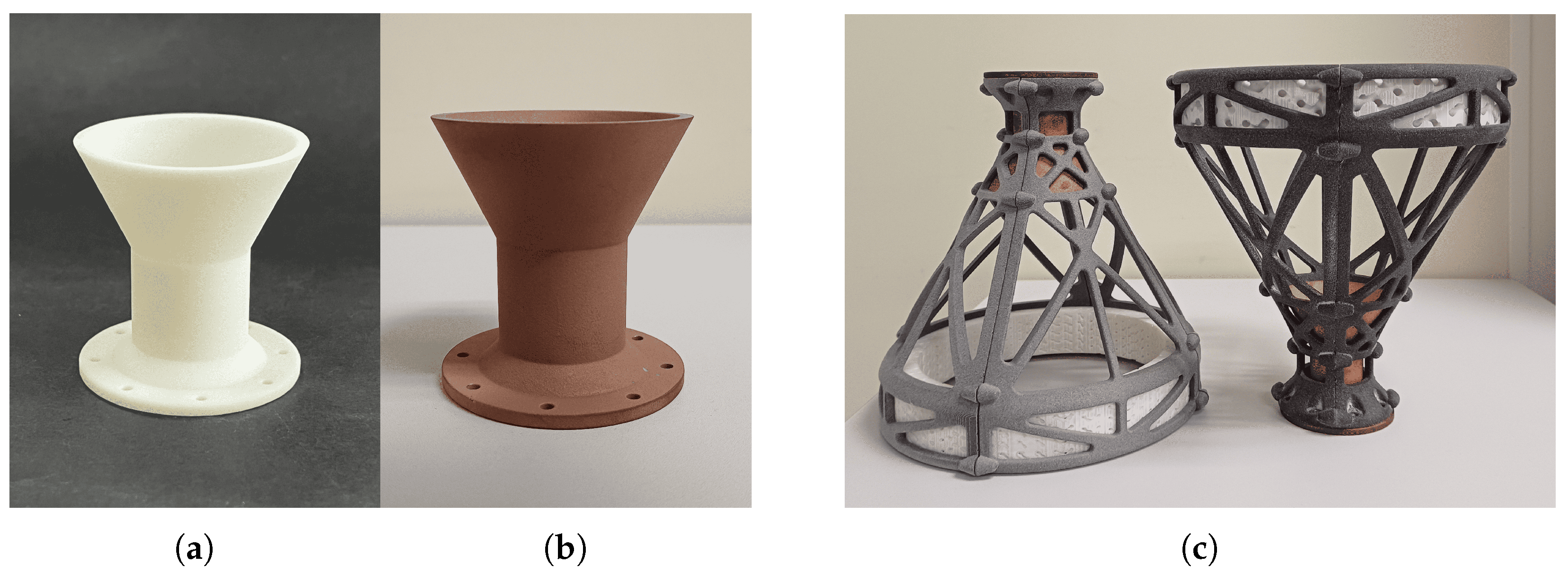
The radiating element is located in the focal point of the set. For the type of communication services the set was intended for (satellite), the whole system would have to handle high power and require low loss; the optimal technology in that case would be waveguide, either rectangular or circular. Traditionally, horn antennas have been used together with waveguides due to ease of integration and high efficiency. In this case, a conic horn was designed to achieve a good balance between illumination efficiency and spillover efficiency. The criterion adopted was that the electromagnetic field level radiated by the horn at the edges of the lens should be 10 dB below the maximum, ensuring an optimal balance between illumination efficiency and spillover efficiency, thereby maximizing the total efficiency of the system. The sketch with the dimensions of the horn is presented in
Figure 8a,b, and the values are provided in
Table 3.
3.1.2. Gradient Index Lenses
The design of the lens covered several stages. First of all, some parameters were chosen in order to meet the sensible size and weight of the whole set. Then, an adjoint method, see [
32], was used to obtain the permittivity values depending on the radius.
The focal point was chosen such that , indicating that the focal length is equal to the diameter of the lens. For practical purposes, the diameter of the lens was D = 15 cm, and its width H = 2.5 cm. That would provide a realizable lens with a low cost AM printer. However, the achievable range of permittivity values was constrained by the available materials and the limitations of the additive manufacturing process. Specifically, printing densities below 20% were avoided to maintain the structural integrity of the lens. Consequently, the feasible permittivity values ranged from to , where represents the relative dielectric constant of the material at 100% density.
On the other hand, not all possible ranges of permittivity could be considered, as the design was constrained by the available materials and the limitations of the printers. A printing density lower than 20% would compromise the structural integrity of the lens. So the possible values ranged from to 0.2(1) + 1, where is the relative dielectric constant of the material printed at 100 % density.
The optimization process determined the optimal distribution of
within a rectangular domain of height
D and width
H. This domain was divided into 11 regions, resulting in 11 levels of freedom where
was constant within each region. Thus, the lens was modeled via the Lippmann–Schwinger integral equation in 2D, as in Equation (
3).
with contrast
and free-space Green’s function
G. The design objective was the field intensity at the focal point
, Equation (
4).
By using the adjoint field
and satisfying Equation (
5),
the gradient with respect to each annular permittivity
was given by Equation (
6).
A quasi-Newton optimizer then updated the 11 discrete until convergence ( or 100 iterations).
The sketch representing the lens with sectors and corresponding values of permittivity is presented in
Figure 8d. It is worth mentioning that the optimized and manufactured lenses presented a central cylindrical sector with a radius of 12.5 mm (which corresponds to the permittivity
) and then the five successive concentric rings with a thickness of 12.5 mm.
The optimizer achieved three different results: a flat heterogeneous lens design, referred to as lens A (
Figure 9a); an airy disk pattern, lens B (
Figure 9b); and a ring pattern, lens C (
Figure 9c). The values of the relative dielectric constant for the different sectors of the three realizations are shown in
Table 4. Both lens B and C present patterns associated with Fraunhoffer diffraction through circular apertures.
3.2. Mechanical Design
The feeding horn antenna and the lens were assembled using a mechanical support. The support was required to provide structural resistance without affecting electromagnetic performance of the antenna, promote the modularity of the system, as well as allow for the exchange of the three types of lenses. The dimensions of the support are outlined in
Figure 8c and their values are given in
Table 3. A four-piece design was chosen, with the pieces connected by pegs, allowing for easy assembly and disassembly. Additionally, to reduce the weight of the support while maintaining its structural resistance, it was designed as a series of rods connected by St. Andrew’s crosses, as shown in
Figure 10. The mechanical support was designed using Solidworks v.2025 software.
3.3. Electromagnetic Impact of Support Structure
To assess the scattering and diffraction effects of St. Andrew’s cross lattice support, we conducted two complementary studies:
Full-wave simulation: The CST model was executed twice—once with the support structures included, and once with them omitted. A comparison of the resulting far-field patterns at 10 GHz showed a maximum change in main-lobe gain of 0.3 dB and an increase in sidelobe levels of no more than 0.5 dB. No additional lobes or ripples were observed.
Experimental measurement: Using an anechoic chamber, we measured the radiation pattern of the lens–horn assembly both with and without the printed support. The resulting patterns aligned within ±0.4 dB across the entire angular range, confirming the simulation findings.
These results demonstrate that the selected lattice geometry and materials (PA11 and UPP) introduce minimal electromagnetic interference. Consequently, the support structure has a negligible impact on the overall antenna performance.
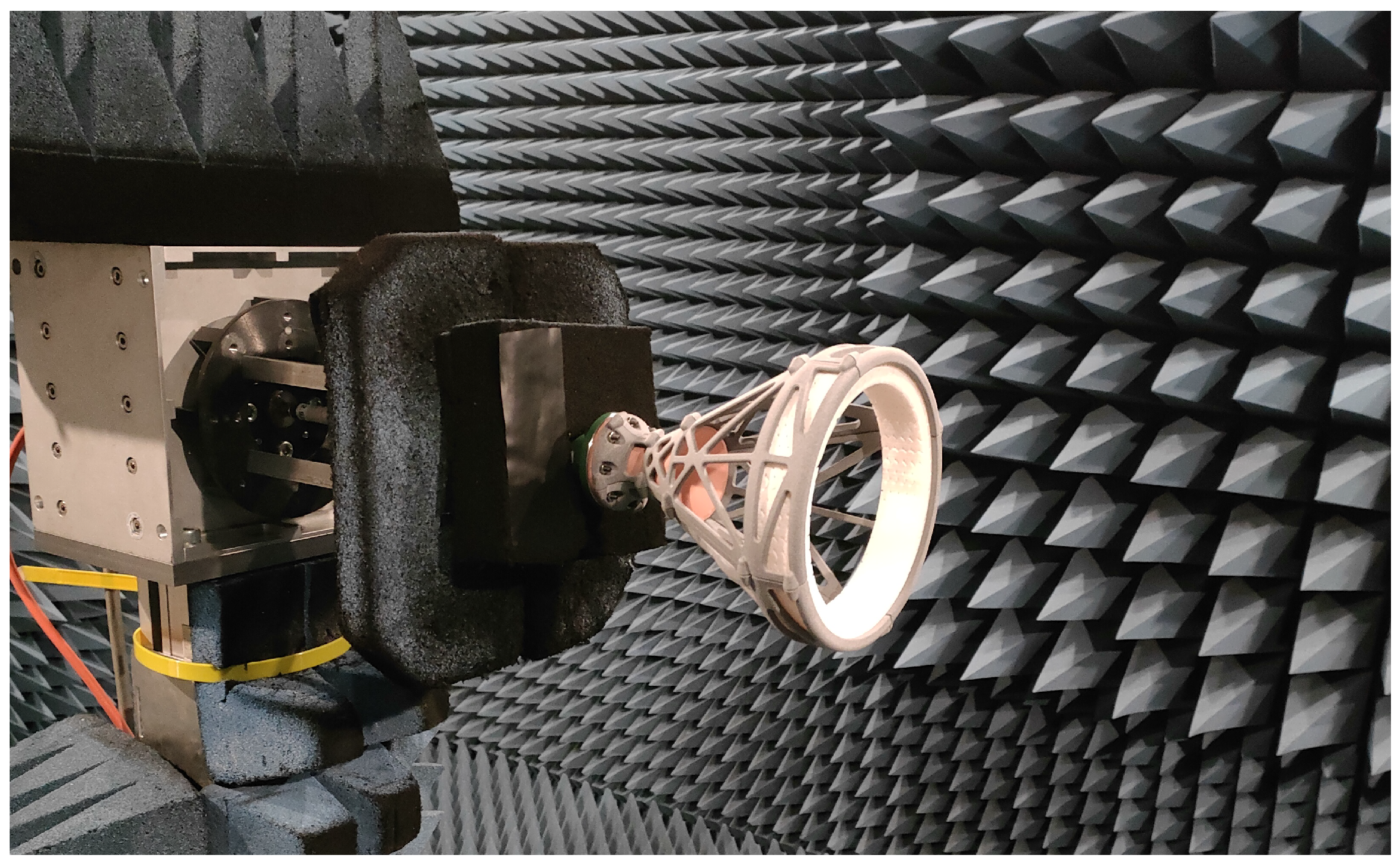
5. Results
The electromagnetic response of the assembled prototypes was evaluated in an anechoic chamber, with the experimental setup depicted in
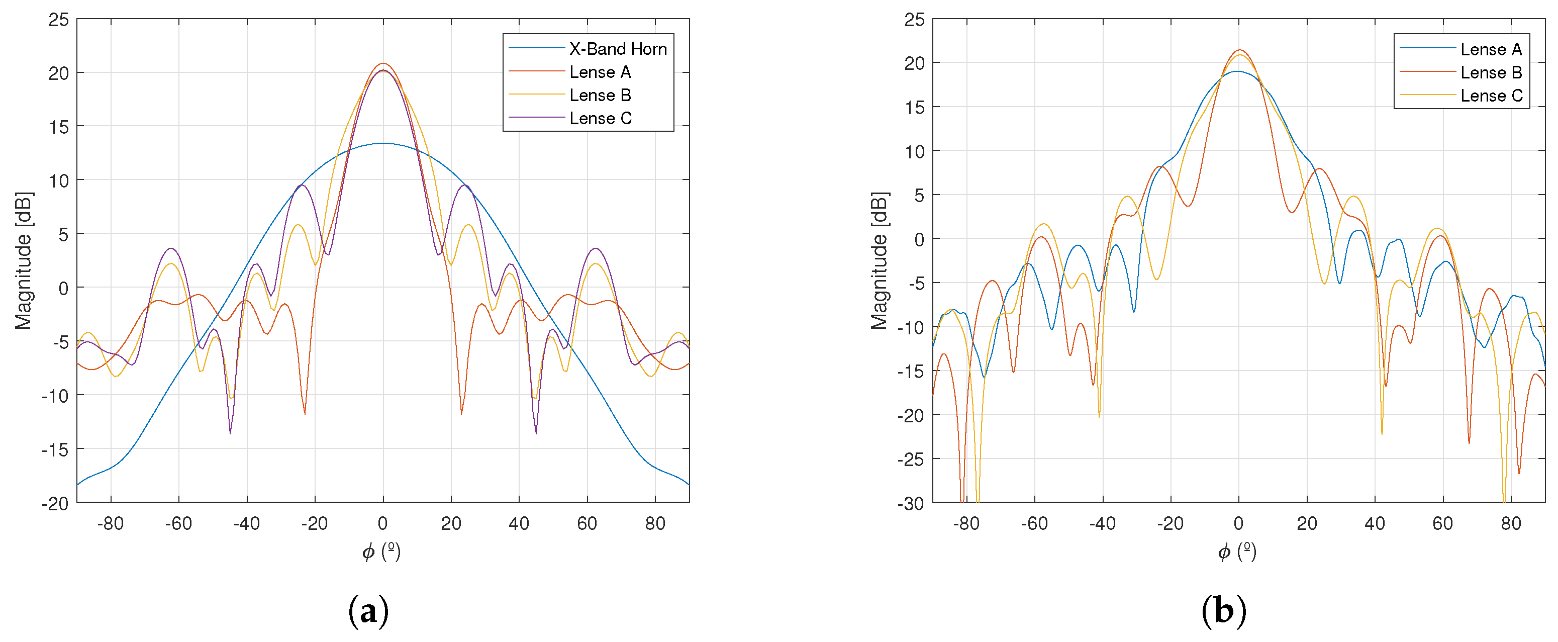
Figure 11. The simulated directivity of the horn antenna and the set with the three different lenses, using the CST Dassault Systems Suite, is presented in
Figure 12a. Therefore, the horn directivity at the maximum of the radiation (
) is 13.4 dB. By adding lenses to the radiation set, a substantial increase in directivity is achievable (up to total directivity of 21 dB for lens A and 20 dB for lenses B and C). The directivities of the different lens antennas were measured and their results are given in
Figure 12b. Regarding lens A, the achieved directivity is 19.5 dB, less than the 21 dB predicted by the simulation. This is most probably due to the fact that the lens was manufactured in four separate pieces. Therefore, airy gaps may appear due to an imperfect mechanical assembly, see
Figure 9a, so the degradation in the farfield measured directivity response is observed. Regarding lenses B and C, the simulation results match very well, even with better results, showing a slightly more directive radiation pattern in the maximum (22 dB for lens B and 22.1 dB for lens C at
).
Additionally, the lenses, as well as the horn antenna and the support, were weighed, with the results presented in the
Table 5. As shown, both the horn antenna and the support are very light, with the lens providing the main contribution to the overall weight. The total weight of the sets ranges from approximately 500 g for lens A to 280 g for lens C.
Table 6 displays the results of our three lenses, which are compared to the recent literature. The main conclusion is that the lenses present similar measured directivity. Lenses B and C present similar or better aperture efficiency compared to the lenses with similar sizes but with an important reduction in thickness, which substantially decreases the volume of the whole set. This is achieved by using variable densities of the printing material in different sectors with consistent thickness, instead of varying the lens thickness—a traditional approach for these lenses. This approach also enhances lens aperture efficiency, as evidenced by our measured results.
6. Conclusions
In this work, we have designed, fabricated, and experimentally validated three GRIN-lens realizations for a compact X-band horn-lens assembly. Experimental measurements showed that lens B achieved the highest performance—measured directivity of 22.1 dBi and aperture efficiency of 55.8%—with a total lens weight of 207 g, see
Table 5. Consequently, lens B is identified as the optimal solution for the envisaged compact X-band satellite-communication application. This result demonstrates the effectiveness of full-wave adjoint optimization, coupled with additive manufacturing, in producing application-specific high-performance RF components.
Furthermore, the GRIN-lens antenna presented in this work was designed for terrestrial satellite–ground communications, where environmental conditions (temperature, humidity, and mechanical loads) remained within the operational limits of polymer-based 3D-printed dielectrics. Nevertheless, the study of 3D-printed materials for RF Applications in space flights is a current trend [
43]. It was demonstrated that the metallized polymeric materials (Rigid 10K and Composite-X), as used here, can be space-qualified [
44]. As for other polymers used in this work, they may exhibit significant outgassing in vacuum and cannot withstand the extreme thermal cycling encountered in space, so further research is required. Consequently, the GRIN-lens antenna design proposed in this work may be suitable for deployment on the payload of a satellite, with substantial modifications. Future adaptation for spaceflight would require substituting the polymer GRIN lens with space-rated dielectrics (e.g., ceramics or radiation-hardened glasses), along with full vacuum, thermal-vacuum, and radiation qualification [
45].
In conclusion, the exploration of AM for fabricating complex RF components—such as horn antennas and GRIN lenses—is not only feasible but also advantageous for the communications industry. By enabling the integration of lightweight, customizable, and precisely engineered polymer structures with metalized conductive elements, AM provides a versatile platform for advanced RF device design. The ability to control material properties and topology on a fine scale, particularly for gradient-index lenses, represents a key advancement in wave manipulation and antenna performance. As the field of AM continues to evolve, its application in communications is likely to expand, supporting the development of more sophisticated, compact, and efficient systems across a range of frequencies and applications.


 ,
, 


