1. Introduction
In many industries, wire coating plays a vital role in providing protection and meeting specific functional needs. However, there are instances where removing these coatings is necessary based on specific requirements. This paper aims to identify an efficient alternative to existing methods, which are often time-consuming and lack precision, especially for microscale wires. These ultra-fine wires are critical in sectors such as aerospace [
1], automotive [
2], and biomedical [
3], where they are utilized in various high-performance applications.
Ultrasonic stripping is a commonly used technique for removing wire coatings by generating cavitation in a liquid medium using high-frequency sound waves [
4]. In this process, the wire is submerged in a fluid, typically water or a solvent, while ultrasonic vibrations produce microbubbles. When these bubbles collapse, they release energy in the form of localized shock waves that strip the coating material without direct contact [
5]. However, due to the extremely small diameter of ultra-fine wires, even these relatively mild shock waves can cause physical stress, leading to issues such as bending, erosion, or breakage. Moreover, it is challenging to target specific sections precisely, limiting the method’s effectiveness for selective stripping [
6,
7].
Chemical stripping involves using solvents or reactive chemicals to break down the insulation material for easier removal [
8]. This method is suitable for coatings that are difficult to handle with mechanical or thermal approaches. However, on ultra-thin wires, it can result in uneven stripping or leftover residue, compromising surface quality [
9]. It also lacks spatial selectivity, as the chemicals affect the entire submerged area. Safety concerns and potential damage to the wire’s integrity further reduce its suitability for precision applications [
10].
Laser stripping offers a non-contact, highly controllable solution for removing coatings using a focused beam of light. This technique provides excellent precision, particularly valuable in sensitive fields such as aerospace, microelectronics, and medical devices [
11]. Unlike chemical or ultrasonic methods, laser ablation avoids mechanical stress and eliminates the need for hazardous chemicals. It enables targeted removal from specific regions of ultra-thin wires without damaging the surrounding area [
12,
13]. The process can also be integrated into automated systems, enhancing overall efficiency, reducing labor requirements, and improving consistency [
14]. Additionally, laser parameters such as power, pulse duration, repetition rate, and focal size can be precisely adjusted to suit various coating materials and geometries [
15,
16]
A key feature of laser ablation, like ultrasonic stripping, is the generation of shock waves. In laser ablation, short high-energy pulses cause rapid heating and plasma formation, producing explosive material ejection and shock wave propagation in the surrounding medium. In ultrasonic methods, shock waves result from the collapse of cavitation bubbles due to acoustic vibration. While their mechanisms differ, both methods rely on rapid energy release and high-pressure waves to remove material. Notably, laser ablation in water helps dissipate heat and control shock wave intensity, offering better protection for delicate substrates and improving process precision.
Notably, various laser parameter configurations have been employed for coating removal on delicate samples across a broad wavelength spectrum, from IR to UV, utilizing technologies such as CO
2, active fiber, active disk, and Nd-YAG (Neodymium-doped Yttrium Aluminum Garnet). The quality of the stripping process is typically evaluated based on surface topography and chemistry. In assessing process performance, samples are subjected to mechanical testing through tensile peeling, with results compared in terms of quality, productivity, and material removal efficiency [
15].
This study investigates the effectiveness of a low-power (3 W) UV laser with a wavelength of 355 nm, optimized by adjusting the pulse width and repetition rate at the lowest range to maximize process accuracy in removing polyamide coatings from fine pure platinum wires. Various ambient conditions were applied to achieve the highest surface quality and precision in targeted areas.
2. Materials and Methods
The samples used in this study are ultra-fine platinum wires with a core diameter of 50 µm, coated with a 15 µm layer of polyamide, resulting in a total outer diameter of approximately 65 µm. Polyamide insulation enhances mechanical durability and provides critical electrical isolation between adjacent wires, preventing microscale contact and signal interference. For PCB (printed circuit board) integration, one end of each wire requires complete coating removal to allow for soldering. This process demands a clean, debris-free platinum surface with low roughness to ensure a reliable electrical connection. As these components are used in high-precision aerospace applications, all steps are subject to strict quality control. The polyamide has a thermal degradation threshold above 400 °C, while platinum offers a high melting point of 1768 °C and excellent thermal conductivity, making it suitable for localized thermal processing. This contrast supports the feasibility of UV laser ablation for selective insulation removal without damaging the substrate, provided laser parameters are carefully optimized.
The laser used for the ablation process is a diode-pump solid-state laser (DPSS) from MACTRON, with a wavelength of 355 nm, average power of 3 W, tunable repetition rate range of 20–200 kHz, and a minimum pulse duration of 18 ns. The reason for choosing this machine is that the short wavelength of UV lasers is highly absorbed by the polyamide coating, which allows for precise energy transfer to the coating while minimizing heat diffusion to the underlying substrate. This machine operates in pulsed mode with short pulse durations, which reduces thermal accumulation in the surrounding material. This is critical for protecting the integrity of the platinum substrate during ablation. On the other hand, the interaction of UV light with water enhances the ablation process by creating cavitation bubbles, which assist in cleaning and thermal management [
6,
7].
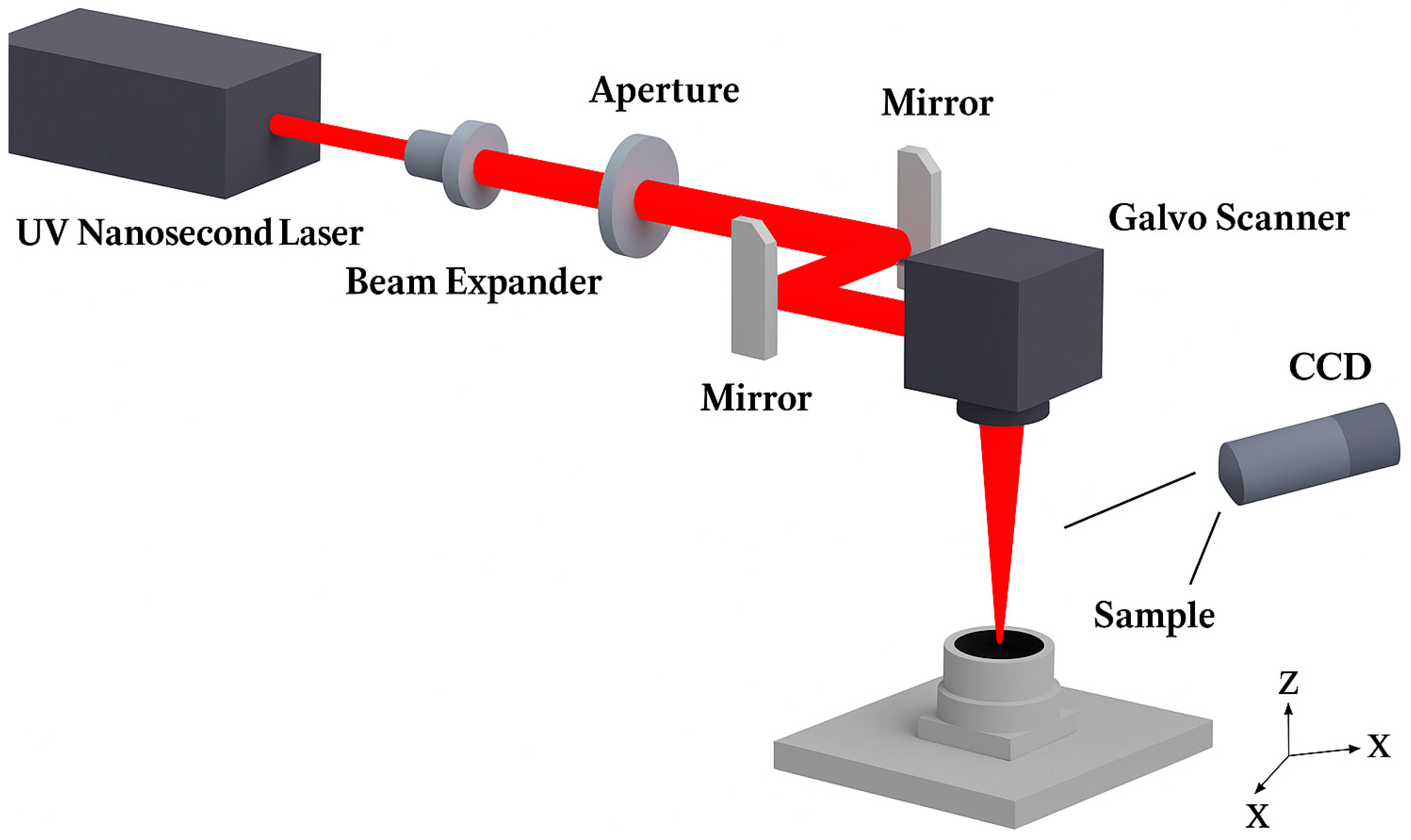
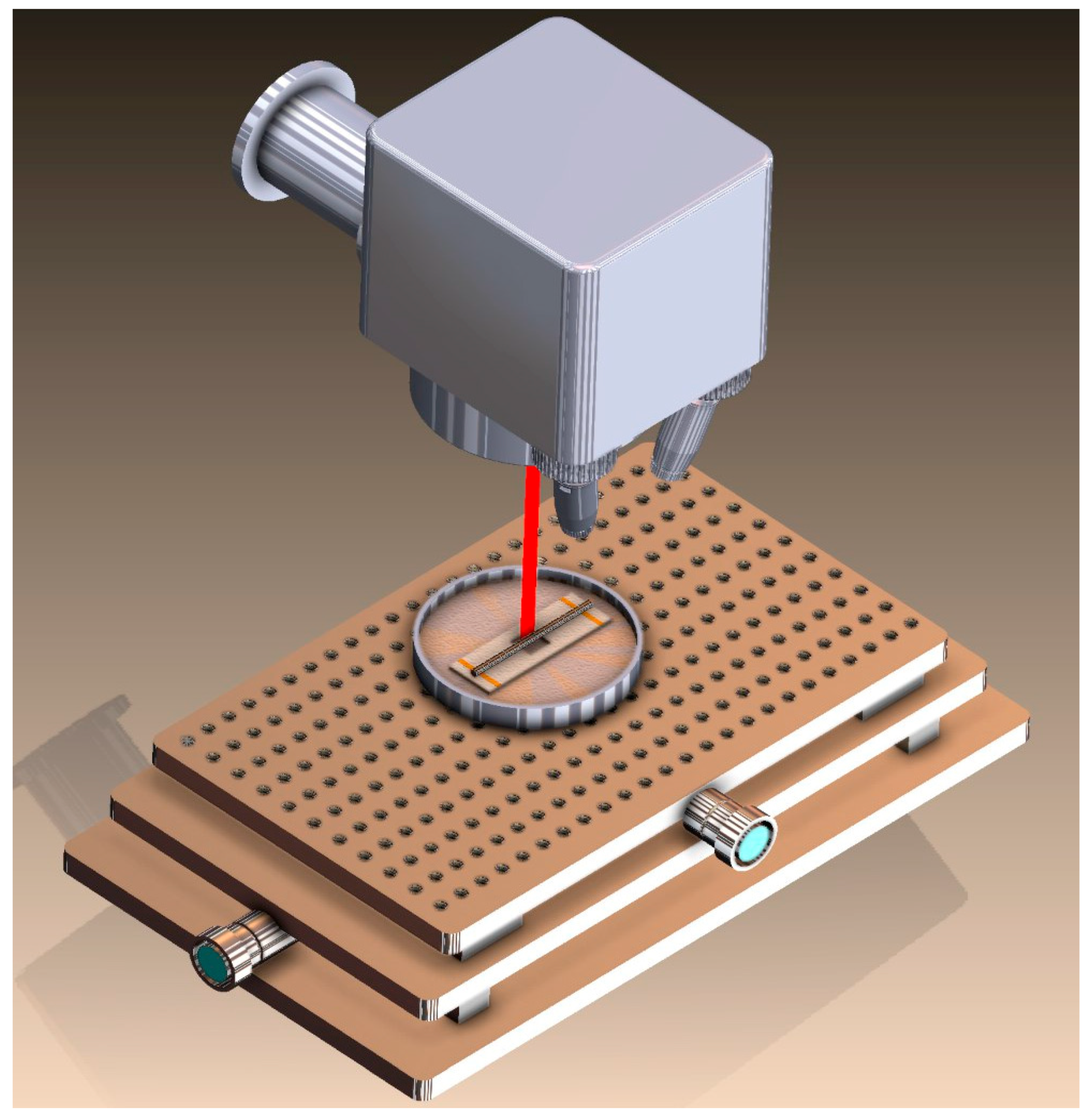
The experimental setup is illustrated in
Figure 1. The laser beam passes through the galvanometer scanner mirrors along the X- and Y-axes. Further, the beam is focused using an f-θ lens of focal length 130 mm, resulting in a final spot diameter of 20 μm at the focal point. Given the fineness of the wires, the objective is to remove the coating while avoiding any damage to the substrate and ensuring the highest accuracy. Therefore, the pulse width and repetition rate were set to the lowest values, at 18 ns and 20 kHz, respectively. For the laser system that emits Gaussian-shaped pulses, with the pulse duration measured at Full Width at Half Maximum (FWHM), the peak laser power is calculated as 8.333 kw using Equation (1) without any correction factor [
17].
Another crucial parameter is the laser fluence (F), the laser energy applied to a specific area of wire (Equation (2)). Fluence represents the energy delivered by the laser over a given area, which is crucial for processes like material ablation [
15,
16,
17].
Based on the performed calculations, the laser fluence used in the experiments is established as 95.5 J/cm2. This value remains consistent across all trials, given the uniform geometry and surface area of the wires, along with the confirmed repeatability of the laser system. However, it is important to note that this fluence was initially calculated assuming a spot diameter of 20 µm. In the subsequent section, it will be demonstrated that this diameter may vary, which directly influences the fluence value.
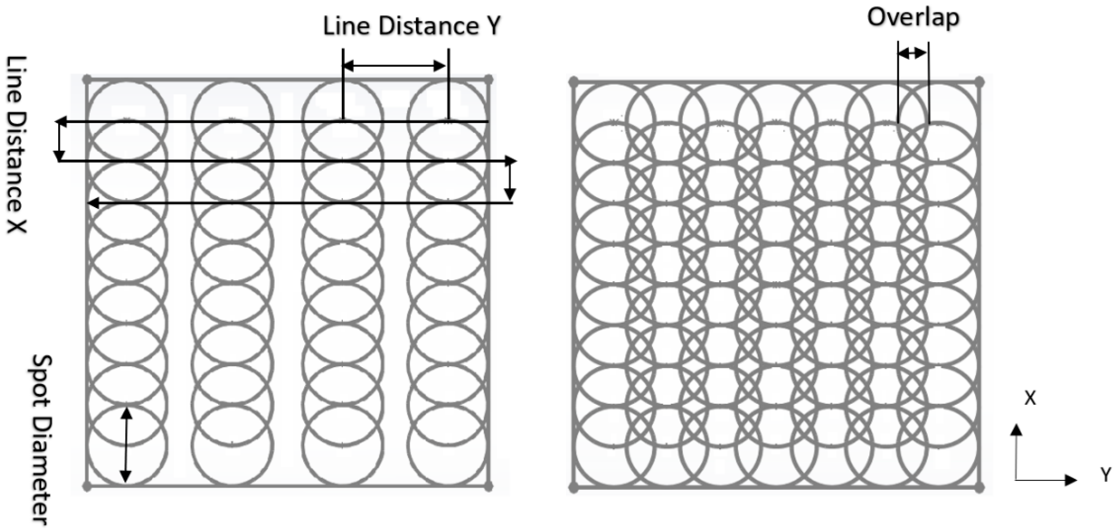
The speed of the Galvano mirror on one axis during the raster scan directly influences the percentage overlap between subsequent spots, as shown in
Figure 2, which, on this machine, on the Y-axis, overlap happens with low speeds. After the first line is complete, the second mirror moves on the orthogonal axis to position the laser spot for the subsequent line scan. This is controlled by the line distance (X) as shown in
Figure 2. The spot overlaps during ablation means that each laser spot deposits energy over a substantial portion of the previously processed area [
18,
19]. The overlap between adjacent laser spots can be determined using Equation (4), which shows how adjusting the line spacing on X controls the overlap along the X-axis.
This increased energy density can improve the efficiency of the ablation, resulting in deeper and more effective material removal. Additionally, this overlap contributes to a smoother surface finish by minimizing irregularities. However, the high level of overlap also results in excessive material removal, which might increase the surface roughness. The localized heating from overlapping passes can increase the temperature of the specimen significantly, creating a larger heat-affected zone (HAZ). Moreover, this excessive heat may lead to issues such as localized melting, warping, or changes in the material properties [
20].
Initial experiments were conducted using large line distances (10 µm and 20 µm) as well as low value of overlap at different speeds to evaluate their effect on the ablation process. Microscopic analysis of the ablated samples revealed that heat primarily affected the coating, with no significant evidence of material removal. Based on these observations, the laser parameters were adjusted, and 12 sets of experiments were conducted. These experiments were initially performed in air, which involved four different speeds, two-line distances, and varying numbers of loops, as outlined in
Table 1. The results were analyzed to assess their impact on surface quality, roughness, and tensile strength, and were benchmarked against wires de-coated using a chemical process.
The wire was aligned parallel to the Y-axis, while the laser scanning operation occurred along the X-axis. Movement in the X direction was managed by the galvanometer scanner, enabling precise control of line spacing, which was set to either 1 µm or 5 µm, corresponding to overlap percentages of 95% and 75%, respectively. In contrast, motion along the Y-axis was governed by the scanning speed, which was carefully adjusted and calculated using Equation (5). This dual-axis control system allowed for precise manipulation of overlap and spacing, ensuring optimal ablation conditions tailored to the experimental requirements.
For example, at a scanning speed of 500 mm/s (500,000 µm/s) and a repetition rate of 20 kHz (20,000 Hz), the center-to-center spacing between successive laser spots along the Y-axis is 25 µm. Given the laser spot diameter of 20 µm in air, this spacing results in insufficient overlap and visible gaps along the Y direction.
Notably,
Figure 2 illustrates the overlap for the ablation process, highlighting the line distance in the X direction (controlled by the galvo scanner) and the spot spacing in the Y direction (determined by the scan speed and repetition rate). The figure represents the actual overlap, where the X and Y direction spacings differ due to distinct control mechanisms. This variation was carefully considered during the analysis and does not compromise the overall effectiveness of the process.
To ensure precise and uniform line spacing, the galvo scanner positioning was synchronized with the laser pulse repetition rate. This synchronization was critical for maintaining the accuracy of the ablation process, especially at higher speeds, and for achieving consistent overlap as depicted in
Figure 2.
It is notable that the line distance in the Y direction could be reduced by increasing the repetition rate. However, observations from multiple sets of experiments indicate that this approach compromises the accuracy of the process and can damage the substrate due to the higher number of pulses and increased energy delivered to the wires. Therefore, it was initially decided to set the pulse width and frequency to their lowest possible values to achieve maximum precision.
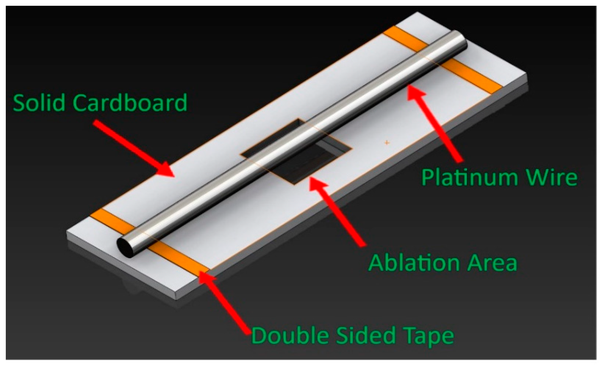
All experiments were conducted with the wires secured using double-sided adhesive tape onto a cardboard holder containing a 10 × 10 mm central window, which enabled precise exposure of the wire segment to the laser beam, as illustrated in
Figure 3.
After completing each experiment, tensile strength was tested using an Instron machine equipped with a 50 N load cell, while surface roughness was evaluated with the Olympus Lext 5000, Tokyo, Japan, confocal microscope.
3. Results and Discussion
3.1. Surface Quality (Air Ambient)
The samples were subjected to ablation in an air medium, and the results were analyzed and compared against those obtained through chemical methods, which served as the benchmark for this study. All images were captured using a confocal microscope equipped with a 20× lens, covering an area of 645 × 648 µm (as shown in
Figure 4). As depicted in
Figure 5, the chemical process successfully exposed the platinum surface without causing any damage to the substrate or deformation. To conserve space, images of the samples following the ablation process were cropped for inclusion in this article.
Moreover, experimental observations revealed that wires ablated at lower scanning speeds and lower line distance X exhibited significant blackened regions due to excessive heat deposition. This heat accumulation not only resulted in the loss of base material but also caused substantial damage to the wires, rendering them extremely fragile, as shown in
Figure 5. At a scanning speed of 500 mm/s, combined with line distances of 1 µm and 5 µm, the wires experienced thermal damage. This suggests that lower scanning speeds, when paired with small line distances resulting in higher overlap, can lead to substrate degradation. Therefore, carefully balancing scanning speed, line distance in the X direction, and the number of passes is essential to achieve optimal ablation performance without compromising wire integrity.
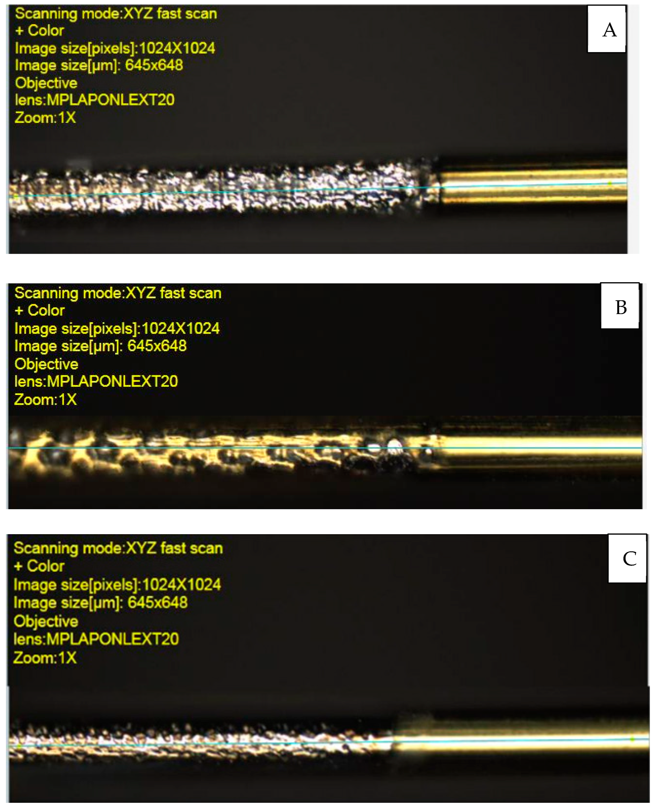
Further adjustments made in air, as shown in
Figure 6, demonstrate improved results compared to earlier trials. However, it is evident that in all cases, the coating was not completely removed, and the wire surface remained excessively rough, indicating an insufficient machining process.
Figure 6A illustrates the ablation performed at a speed of 1000 mm/s with the smallest line distance (1 µm) and 95% overlap. While the coating was partially removed, the surface quality was significantly inferior to that achieved through chemical processing.
In another setup (
Figure 6B), the scanning speed was increased to 1200 mm/s, and the overlap was reduced by increasing the line distance to 5 µm. Additionally, the wires were exposed to two laser passes. As shown, this configuration resulted in less thermal damage to the substrate; however, the coating was removed in a segmented pattern. This discontinuous removal can be attributed to insufficient overlap in the Y direction, where the increased scanning speed led to a center-to-center spot spacing of approximately 60 µm. Although this adjustment helped reduce thermal stress and better-preserved wire integrity, it was still inadequate for achieving complete and uniform coating removal. This highlights that while increased speed and reduced heat input mitigate damage, they must be carefully balanced with overlap and energy density to ensure effective ablation.
Finally, the speed was set to 1500 mm/s with 95% overlap (line distance 1 µm) to test whether a smoother surface could be achieved by combining a larger line distance in the Y direction and a lower line distance in the X direction. As shown in
Figure 6C, this adjustment resulted in improved wire integrity and reduced damage. However, the surface quality remained unsatisfactory, with high roughness values, as discussed in the following section. Additionally, several samples from the design of experiments showed incomplete coating removal, with the ablation affecting only part of the surface. These samples were deemed unsuitable for further scanning or experimentation due to their compromised condition. In conclusion, due to the sensitivity of the sample, complete coating removal was critical, rendering these adjustments unsuitable. Specific parameters for each wire are detailed in the corresponding figure descriptions.
3.2. Tensile Strength (Air Ambient)
Tensile strength measurements were conducted using a Universal Testing Machine (UTM) following the removal of the polyamide insulation. After laser ablation, the wire specimens adopted a dumbbell-like geometry, with a 10 mm central section stripped to expose the bare platinum core (50 µm in diameter), while the insulated ends (65 µm in diameter) were retained to facilitate secure clamping. Although most parameter sets did not result in complete coating removal, the ablated regions showed significant changes in both geometry and surface condition compared to the original state. It is important to note that, due to incomplete or inconsistent coating removal in the majority of tested conditions, the effective cross-sectional area of the wire could not be precisely determined. Consequently, tensile strength is reported in gram-force (gf), directly representing the applied breaking load. Conversion to stress units (MPa) was only performed for the condition in which the platinum core was fully exposed and structurally uniform, allowing for a reliable calculation based on known cross-sectional area.
Figure 7 presents the tensile strength results for various ablation parameters. All samples were prepared with consistent lengths, and the coating removal process followed standardized protocols. To ensure measurement accuracy and eliminate slippage, the wires were firmly gripped in the UTM fixtures.
The results indicate that chemically de-coated wires exhibited an average tensile strength of 115 gr.f as shown in
Figure 7. In contrast, wires ablated at 500 mm/s in air were excessively fragile and prone to breakage, rendering them unsuitable for mounting and testing on the UTM. Samples processed with a line distance of 5 µm and a single laser pass exhibited minimal thermal effects; however, they failed to achieve sufficient coating removal. As only superficial ablation tracks were observed on the surface, these samples were deemed unsuitable for tensile testing and considered ineffective for practical evaluation. Observations across multiple samples, conducted to ensure process repeatability, revealed that a lower percentage of overlap combined with a single loop, for low speeds, was insufficient for effective ablation.
The remaining samples demonstrated sufficient stability to be mounted on the UTM grips, and their tensile strengths were successfully measured.
Figure 7 presents a comparison of tensile strength across different ablation settings in the air environment and chemical serving as a reference. However, the results for ablated wires were consistently lower than those of chemically de-coated samples.
It should be noted that three samples were tested for each setting, and the figure presents the average tensile strength along with corresponding error bars.
While the tensile strength at higher speeds and lower overlap percentages may seem adequate, it is important to note that the surface quality of all air-ablated samples was unsatisfactory, and the stripping process was incomplete. Ultimately, the process was ineffective due to incomplete coating removal, leaving the surface quality unsatisfactory.
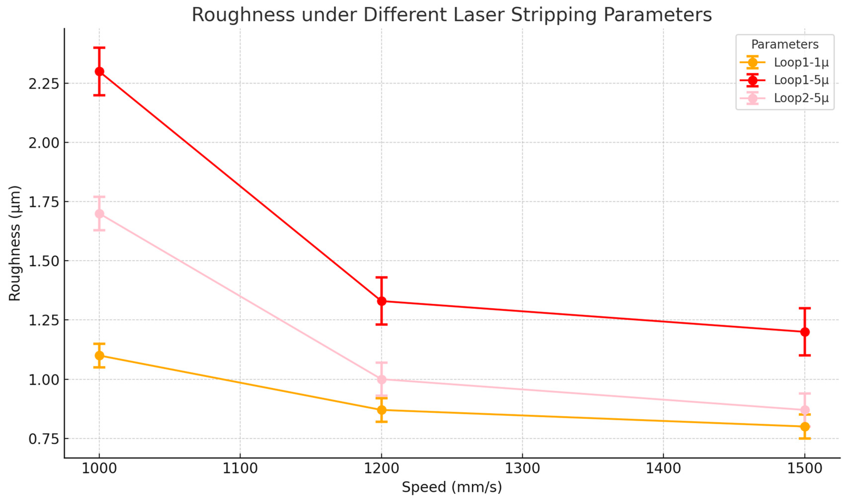
3.3. Average Roughness Ra (Air Ambient)
Surface roughness of the samples after material removal was analyzed using a Confocal Olympus Lext 5000, in compliance with the ISO 25178 standard [
21] to ensure consistent surface texture assessment. The measurement range was between 645 µm and 648 µm, which is within the capacity of the system used. Ra was primarily determined through 3D profilometry; additional measurements were taken at various orientations to verify consistency. For each wire, roughness measurements were taken at three distinct segments: the two transition borders and the center of the ablated region. This process was performed on three wires for each laser adjustment. The three segment values from each wire were averaged to obtain a single roughness value per wire. These three values (one per wire) were then used to calculate the average and standard deviation presented in the roughness plots.
Figure 8 illustrates the roughness measurements obtained from the ablated regions. Conducting roughness measurements for all ablated samples was not feasible, as wires processed at speeds below 500 mm/s exhibited significant burning and cracking, evident through visual inspection. As shown in
Figure 8, the roughness of the ablated wires was substantially decreased when a line distance of 1 µm was employed, in contrast to 5 µm.
This observation suggests that higher overlap yields smoother surface quality, though it negatively impacts tensile strength. The damage observed in these ablated areas can be attributed to excessive heat exposure during the process. On the other hand, the surface roughness (Ra) can be minimized by employing higher ablation speeds, which mitigate heat concentration. Additionally, conducting laser ablation in multiple loops when the overlap was 75% enhances surface smoothness. With each pass, a small layer of material is removed, enabling progressive surface refinement and partially compensating for the reduced overlap. This iterative approach provides a balance between smoother surface finishes and minimizing damage caused by heat.
After measuring the roughness average (Ra) for all samples ablated in air, the results varied between 0.76 and 2.4 µm. In contrast, the chemically stripped wires exhibited an average Ra of 0.1 µm. This significant discrepancy suggests that the surface roughness of the laser-ablated wires should ideally be much lower, approaching that of the chemically treated samples, indicating the potential for achieving a higher quality surface through optimized laser parameters and processing conditions.
3.4. Spot Diameter Consideration
Based on these findings, it is essential to emphasize that, according to the experimental design, the X-axis overlap is high. However, initial calculations suggested that increasing the scanning speed in the Y-axis would lead to a greater distance between consecutive laser spots. For instance, at a speed of 1000 mm/s, the center-to-center distance between spots in the Y-axis is 50 microns. Given the spot diameter of 20 microns in the y-axis certain section of the wire will remain unprocessed (
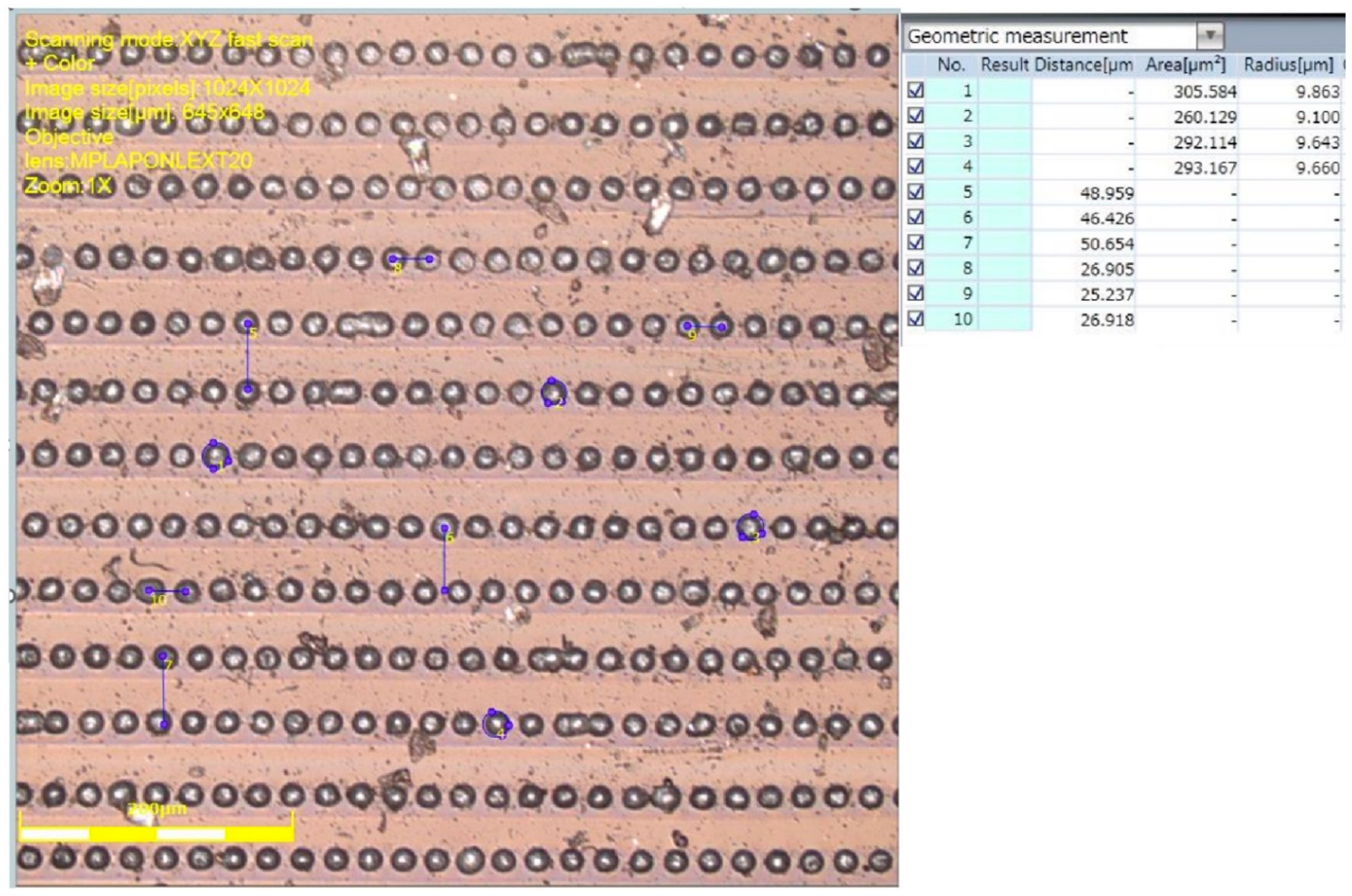
Figure 6B). To validate whether the laser system behaved as predicted, experiments were conducted on a flat sheet with varying speeds and a significant value of X line distance. The results confirmed the initial assumption on a flat surface, ablation in the Y-axis occurred in separate sections, with no overlap, leaving unprocessed regions between laser spots, as shown in
Figure 9. The sheet images were captured using a confocal machine under the same conditions applied to the wires during roughness measurements.
Figure 9 presents a laser-processed sheet analyzed using a confocal microscope, with all measurements obtained through various tools within the machine’s software. Notably, a high line distance in the X direction was deliberately chosen to eliminate overlap, ensuring two key objectives: first, to provide a clearer understanding of the machine’s performance through this visualization, and second, to prevent surface damage that could compromise image quality. The laser speed was set to 500 mm/s, resulting in a 25-micron center-to-center spacing between laser spots along the Y-axis. In the X direction, laser passes occur at 50-micron intervals. As illustrated in the image, noticeable gaps remain in the Y direction between laser spots, confirming that even with a minimal 1-micron line distance in X, overlap occurs only along the X-axis, while gaps persist in the Y-axis.
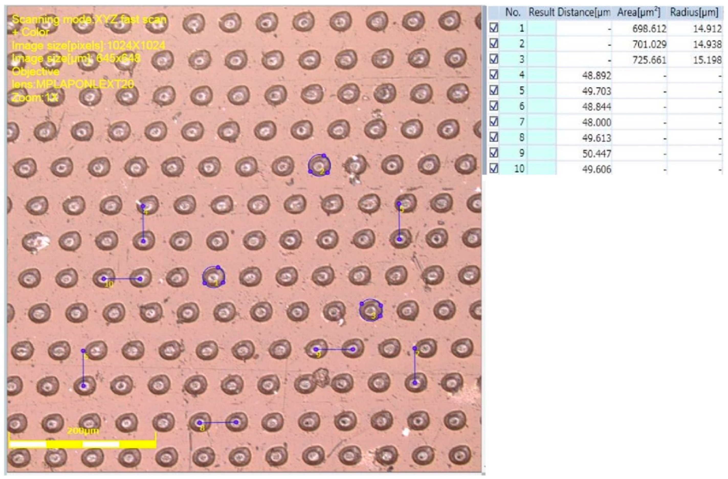
However, when transitioning from a flat sheet to a cylindrical wire, a notable difference in laser interaction was observed. Since the laser beam only affects a semi-circular section of the wire, variations in the beam’s angle of incidence result in different effective focal distances across the curved surface. Given the wire’s 65-micron diameter, the focal point naturally shifts by approximately 32.5 microns along the surface, leading to changes in the spot diameter. To investigate this effect, a 3-milliliter layer of water was added to a flat sheet (to check the effect of water too) and subjected to laser ablation at a speed of 1000 mm/s with a line distance of 50 microns in the X direction. Microscope measurements revealed an average spot diameter of 30 microns and a center-to-center spacing of 50 microns in the Y direction, aligning with theoretical predictions. This also explains why excessive overlap occurred at lower speeds, such as 500 mm/s, where the Y-axis line distance is 25 microns. In this case, the expanded spot diameter exceeded the standard value, leading to significant energy concentration, which caused localized burning and increased susceptibility to fracture. It is important to note that while the X-axis overlap was initially calculated based on a 20-micron spot diameter, practical conditions resulted in an actual increase in spot size. Consequently, the effective overlap percentage was higher than expected. As depicted in
Figure 10, the spot diameter increased to 30 microns at the focal length.
Although the initial 30 µm laser spot size was calculated for ablation on a flat surface in water, the wire processing still used a focal point set at the wire’s apex. This approach did not compensate for defocusing caused by the wire’s curved geometry, which shifts the effective focal position along the surface. To improve coverage across the wire’s circumference, the focal plane needed to be lowered. However, since the machine’s Z-axis could only adjust in 1 cm increments, a MITUTOYO height gauge was used to manually reduce the Z-position by 32 µm, bringing the laser focus closer to the wire flanks. This adjustment aimed to optimize focus and enhance the ablation area. Subsequent measurements with realistic situations confirmed that the average spot diameter had increased to approximately 45 µm. This value corresponds to the largest spot size at the lowest point of the wire’s curvature. Conversely, at the highest point where the focus was originally set, the spot size remains closer to 30 µm. As a result, the effective spot diameter varies throughout the process due to both the curvature of the wire and the adjusted focal plane. Notably, this ablation process was applied to over 180 degrees of the wire’s surface, effectively treating half of its circumference.
In the subsequent ablation trials under water, a 45 µm spot diameter was used. This larger spot size resulted from both the laser’s incident angle and the wire’s 32.5 µm radius, which together caused the beam to spread across the curved surface. These effects increased the effective overlap in both the X and Y directions. Consequently, despite the apparent spacing along the Y-axis, the ablation remained continuous with no unprocessed regions on the wire.
As the spot diameter increased, the fluence of the laser on the wire surface also changed accordingly, based on the calculated values. While the peak power of the laser remained constant at 8.33 kW, the fluence decreased to 18.86 J/cm2, as determined using Equations (2) and (3). This decrease in fluence resulted from the expanded spot size, which spread the same energy over a larger area. Therefore, under the new configuration, the wires were exposed to a lower fluence.
3.5. Surface Quality (Water Ambient)
Following the unsuccessful attempts with air-based ablation, experiments were shifted to a water environment to address the excessive heat generated on the wire surfaces during the laser process. In water-based laser ablation, the rapid vaporization of the surrounding liquid produces bubbles that expand and collapse within microseconds. This phenomenon generates shockwaves, microjets, and vibrations, which exert mechanical forces on the wire surface, facilitating the removal of the coating material. The water layer not only dissipates heat effectively, minimizing thermal damage to the wire substrate, but also enhances the de-coating process through mechanical agitation [
22]. Observations from the air-ablation trials revealed that a lower overlap of 75% (5 µm line distance X) with a single loop was insufficient for effective coating removal, whereas two loops showed improved results. Accordingly, the parameters for the water-based experiments were developed and implemented as detailed in
Table 2.
Immersing the sample in water while maintaining proper support during the laser ablation process posed a significant challenge, as the water level above the wires was found to be a critical parameter. Experiments were carried out using the specified laser parameters within a container of 10 cm in diameter. The samples, each consisting of a 40 mm long wire, were positioned at the bottom of the container, half filled with water to maintain a consistent water layer above the wires. As shown in
Figure 11, the entire setup, including the water container, was mounted on a two-axis workbench positioned beneath the laser system’s camera for accurate alignment and control during ablation.
Microscopic examination of the ablated samples revealed that while the underlying substrate remained intact and partial coating removal was achieved, the results were inconsistent across the wire surface, as illustrated in
Figure 12. In certain regions, the coating persisted, indicating a degree of stochastic behavior in the ablation process. This inconsistency emphasized the critical role of maintaining a stable and optimal water level above the wire during laser exposure.
Furthermore, each ablation cycle led to water contamination with detached polyamide fragments, adversely affecting subsequent experiments. When suspended in water, the stripped coating material exhibited adhesive behavior and often redeposited onto the surface of the next wire, thereby reducing surface quality. To ensure process consistency and repeatability, the water was replaced and the container thoroughly cleaned after each trial.
During laser irradiation, the interaction between the beam and the coated wire in water produced gaseous byproducts, leading to the formation of microbubbles. These bubbles contributed to localized fluid agitation and cavitation phenomena, which played a beneficial role in dislodging and removing surface debris [
22].
In the subsequent phase, water was added to the container until it just reached the top level of the wires, ensuring complete submersion without excess coverage. To establish a controlled water layer above the wires for the ablation process, a milliliter-graduated injector was used to incrementally introduce additional water into the setup. Approximately 2 to 3 milliliters of water were carefully added above the wires, providing the precise conditions required for the experiment.
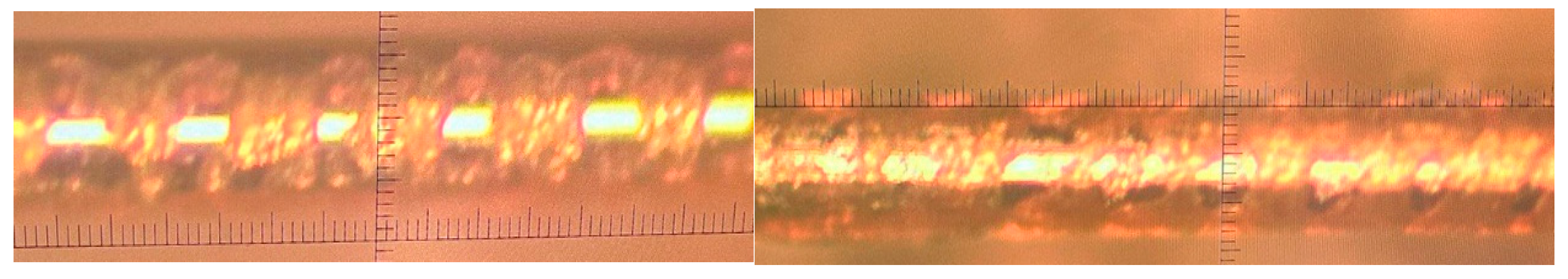
Figure 13 presents confocal images of samples ablated on one side, highlighting the influence of speed and line distance X on process quality. At a speed of 500 mm/s (
Figure 13A), localized damage was evident in certain wire segments, akin to observations made during air-based ablation. This confirmed that such low speeds are unsuitable for fine wires of this nature. At higher speeds, 1000 mm/s with 88.88% overlap and two loops, 1200 mm/s with 97.77% overlap and one loop (
Figure 13B,C), no damage was observed, and the coating was completely removed. However, further increasing the speed to 1500 mm/s led to incomplete coating removal. As mentioned earlier, the increase in speed resulted in a larger line distance in the Y-axis, creating gaps that neither the water layer nor variations in the beam’s incident angle could fully compensate for. Consequently, some regions remained intact. Moreover, the positions of these unablated sections were stochastic, varying from sample to sample due to slight differences in laser interaction with the wire’s surface, regardless of the overlap percentage or number of loops (
Figure 13D).
To ensure uniform coating removal around the full circumference of the wire, the samples were carefully flipped, and the laser focus was readjusted to target the opposite surface. The ablation process was then repeated under the same conditions. As illustrated in
Figure 13E, this dual-sided ablation resulted in complete and consistent coating removal across the wire surface. The image was captured using the on-site optical setup, which consisted of a NIKON Nomarski (Tokyo, Japan) Differential Interference Contrast (DIC) Microscope with 20× magnification, paired with a CALTEX HD60 Camera (Singapore) equipped with a 0.5× lens.
Notably, all roughness measurements and profile analyses were conducted under identical conditions using the same confocal microscope specifications to ensure the integrity and consistency of the experimental results.
Both speeds, 1000 mm/s and 1200 mm/s, combined with 1 µm X-line distance (Overlap of 97.77%) and one loop, resulted in clean, smooth, and residue-free surfaces. The higher speed of 1200 mm/s would be advantageous in terms of time efficiency and a lower value of roughness. The effects of Speed, line distance and the number of loops, together with the analysis of surface roughness and tensile strength will help with the process parameter optimization.
3.6. Tensile Strength (Water Ambient)
Following the ablation process, the wires were dried at room temperature and carefully mounted in the grips of a Universal Testing Machine (UTM). Samples ablated at a speed of 500 mm/s with both line distance settings exhibited significant thermal damage, similar to the degradation observed in air ambient tests. This level of damage rendered the samples too fragile for tensile strength evaluation. Conversely, ablation at 1500 mm/s across all tested parameters failed to achieve complete coating removal, thereby making tensile testing infeasible due to inconsistent surface preparation.
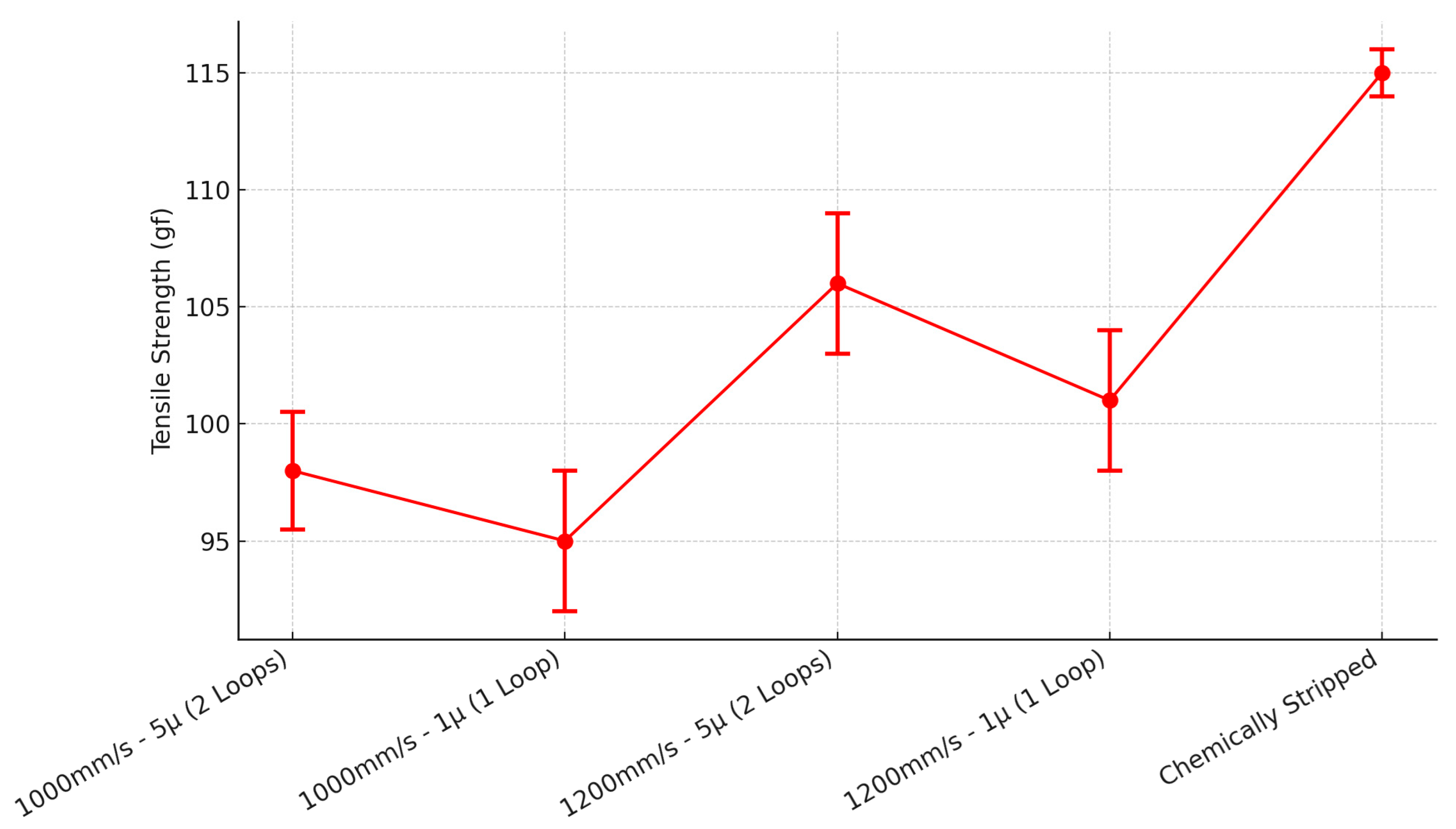
As presented in
Figure 14, chemically stripped wires demonstrated tensile strength average value of 115 gr.f, whereas water-ablated samples at 1000 mm/s
−1 µ showed tensile strength values between 89 and 95 gr.f. Notably, samples ablated at 1200 mm/s
−1 µ exhibited greater consistency, with tensile strength ranging from 98 to 104 gr.f and a mean value of approximately 101 gr.f, which is approximately 12% lower than the mean tensile strength of chemically stripped wires. This enhanced consistency is attributed to reduced thermal effects on the wire surface.
On the other hand, samples ablated with 88.88% overlap in two loops exhibited higher tensile strength. However, visual inspection revealed inadequate surface quality and incomplete coating removal, rendering these samples unsuitable as a final satisfactory outcome for this research.
3.7. Average Roughness Ra (Water Ambient)
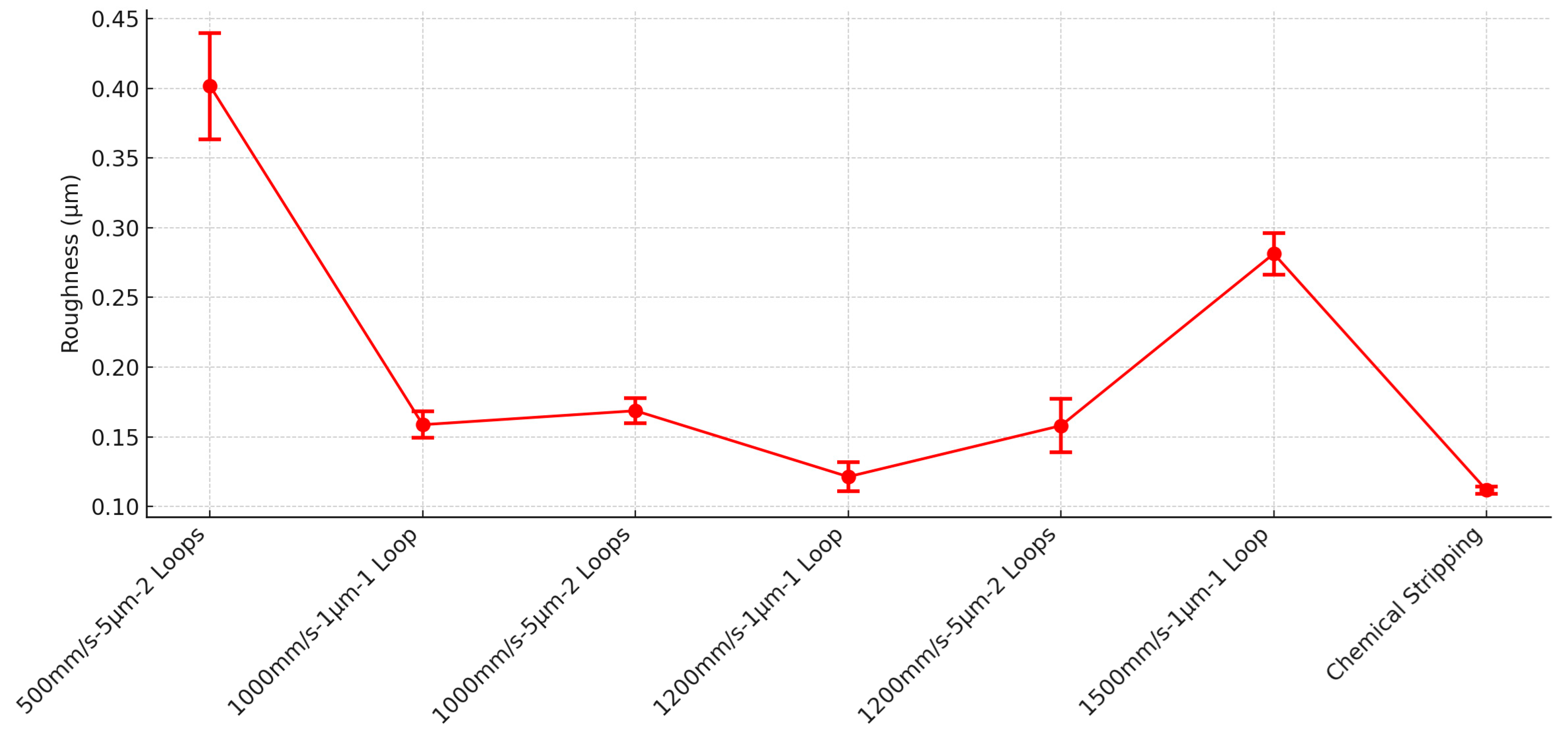
To assess the roughness of the samples ablated in water in comparison with those from chemically stripped samples, three samples from each experiment were examined using a confocal microscope. Each wire was analyzed in three distinct segments, with a range of 645 µm × 648 µm, and the average roughness values were recorded in
Figure 15. Although the chemically stripped samples exhibit a smoother surface quality, the laser-ablated wires in water are still considered satisfactory. The inherent nature of laser processing often alters surface quality, significantly impacting the surface texture of materials. This alteration can lead to various surface characteristics, such as roughness and thermal damage, which may not meet the desired specifications for certain applications [
23]. The key challenge lies in developing a process to control this effect, thereby achieving the desired outcome.
Samples ablated at 500 mm/s using a 5 µm line distance in the X direction with two loops exhibited a relatively high average surface roughness (Ra) of 0.396 µm. This was primarily attributed to significant thermal damage, compromising the wire’s structural integrity. In contrast, ablation at 1500 mm/s with a narrower 1 µm line distance and a single loop led to incomplete coating removal. This left residual material on the wire, resulting in a lower roughness of 0.284 µm. The insufficient removal at higher speed is likely due to the large line spacing in the Y direction, which was not adequately compensated for by the wire’s curvature, the expanded laser spot size, or the water medium. As a result, unprocessed gaps formed between adjacent laser paths.
Interestingly, the data showed that higher scanning speeds tend to produce tensile strength and surface roughness values more closely aligned with those achieved through chemical stripping. If a properly optimized process can be developed by adjusting the overlap along the X-axis and increasing the number of loops, it may be possible to achieve even better surface quality and mechanical performance than with chemical methods. This optimization will be the focus of the next phase of the study.
It is noteworthy that the samples ablated at 500 mm/s with a line distance of 1 µm, even in the presence of water, were severely burned, and the substrate was damaged. Additionally, the samples processed at 1500 mm/s with lower overlap settings (5 µm and 2 loops) also produced unsatisfactory results. The coating was removed inconsistently from section to section, making these parameters impractical, and the measured roughness values under these conditions were not reliable.
Ablation at 1000 mm/s with a line distance of 1 µm (97.77% overlap) produced smoother surfaces with an average roughness of 0.155 µm, representing an improvement over similar tests conducted in air. Notably, ablation at 1200 mm/s with a 1 µm line distance in water achieved a mean roughness of 0.129 µm, approaching the chemically stripped wire’s roughness of 0.104 µm. This suggests that ablation at 1200 mm/s in water provides superior surface quality, likely due to minimized thermal effects. Visual inspection indicated satisfactory results for both 1000 mm/s and 1200 mm/s speeds; however, roughness measurements confirmed that the 1200 mm/s condition yielded a surface quality more comparable to chemically stripped wires. Additionally, the tensile strength achieved under this condition was higher, and the process was more time-efficient, emphasizing the advantages of water-based ablation with a speed of 1200 mm/s with a spacing between passed of 1 µm and a single loop.
4. Conclusions
This study evaluated the feasibility of using UV nanosecond laser ablation to remove polyamide insulation from ultra-thin platinum wires in air- and water-assisted environments. Among the tested parameters, water-assisted ablation at 1000–1200 mm/s with high overlap and a single loop achieved clean, residue-free surfaces comparable to chemical stripping while also preserving the mechanical integrity of the wire. A thin water layer was critical in dissipating heat and minimizing thermal damage to the substrate.
Key factors such as scanning speed, line distance, overlap percentage, and loop count significantly influenced ablation outcomes. Notably, variations in laser spot size caused by wire curvature and water interaction affected energy distribution, highlighting the importance of precise optical calibration.
While chemical stripping generally produced more consistent results, the wires processed under select optimized laser parameters exhibited satisfactory outcomes. These laser-treated wires were successfully soldered onto printed circuit boards (PCBs) during subsequent manufacturing steps, without introducing defects or malfunctions in the final assembled products. This confirms that when carefully tuned, laser ablation can meet structural and functional performance requirements.
In conclusion, this work supports the viability of laser ablation as a selective, controllable alternative to chemical methods for fine-wire processing. Future research should explore additional ablation media and parameter combinations to further enhance efficiency and expand applicability in microfabrication.


