Article

Investigating the Influence of Mechanical Loads on Built-Up Edge Formation Across Different Length Scales at Diamond–Transition Metal Interfaces

by
Mazen S. Alghamdi
1,
Mohammed T. Alamoudi
1,
Rami A. Almatani
1 and
Meenakshisundaram Ravi Shankar
2,*
1
Advanced Materials Technologies Institute, King Abdulaziz City for Science and Technology (KACST), Riyadh 11442, Saudi Arabia
2
Department of Industrial Engineering, University of Pittsburgh, Pittsburgh, PA 15261, USA
*
Author to whom correspondence should be addressed.
J. Manuf. Mater. Process. 2025, 9(6), 176; https://doi.org/10.3390/jmmp9060176
Submission received: 17 April 2025 / Revised: 17 May 2025 / Accepted: 26 May 2025 / Published: 28 May 2025

Abstract

:
Investigating failure mechanisms in cutting tools used in advanced industries like biomedical and aerospace, which operate under extreme mechanical and chemical conditions, is essential to prevent failures, optimize performance, and minimize financial losses. The diamond-turning process, operating at micrometer-length scales, forms a tightly bonded built-up edge (BUE). The tribochemical interactions between a single-crystal diamond and its deformed chip induce inter-diffusion and contact, rapidly degrading the cutting edge upon BUE fracture. These effects intensify at higher deformation speeds, contributing to the observed rapid wear of diamond tools during d-shell-rich metal machining in industrial settings. In this study, these interactions were studied with niobium (Nb) as the transition metal. Tribochemical effects were observed at low deformation speeds (quasistatic; <1 mm/s), where thermal effects were negligible under in situ conditions inside the FEI /SEM vacuum chamber room. The configuration of the interface region of diamond and transition metals was characterized and analyzed using focused ion beam (FIB) milling and subsequently characterized through transmission electron microscopy (TEM). The corresponding inter-diffusion was examined by elucidating the phase evolution, element concentration profiles, and microstructure evolution via high-resolution TEM/Images equipped with an TEM/EDS system for elemental characterization.

1. Introduction

Diamond is widely recognized as the hardest known material used in a natural single-crystal form for high-speed finishing processes [1,2,3]. However, single-crystal diamonds may exhibit unpredictable early failure (wear) [1,4], which is a common issue among various cutting tools. Wear in diamond tools can arise from a combination of mechanical, chemical, and physical mechanisms [5]. These mechanisms include adhesion, abrasion, microchipping, fracture, fatigue, tribothermal wear, and built-up edge (BUE) formation, the latter of which is influenced by machining parameters such as the cutting speed and depth of cut [3]. These factors increase the temperature at the interface of the contacted area between cutting tools and machined pieces, leading to adhesion and strain hardening between the cutting tool and the workpiece [6]. Tribochemical wear, which occurs under the combined action of mechanical and chemical forces, has been extensively studied in turning processes involving single-crystal diamond tools and non-diamond materials such as niobium (Nb), titanium (Ti), and zirconium (Zr) [7,8,9,10]. This wear often manifests as deformation on the rake edge when material builds up against the diamond’s surface during machining. Significant strain generation occurs during severe plastic deformation (SPD) via chip formation, as observed in machined samples like copper (Cu) [5]. Understanding these wear mechanisms is essential for mitigating machining conditions that lead to wear phenomena, emphasizing that wear is not an inherent material property, but a reaction to various operational factors [11]. Wear generated from technical contact is a categorized sliding, rolling, impact, fretting, or abrasive slurry action. These deformations result from the contact between two solid materials, which can lead to plastic or elastic contact [12]. Adhesive, abrasive, and fatigue wear are common types that arise under these conditions [13]. Each type occurs under plastic or elastic contact, as seen in corrosive wear [13]. Corrosive wear arises under plastic contact, leading to tribochemical wear that enhances diffusion [12,14] at the contact area interface of the diamond tool and the machined piece. Tribochemical wear is a complex system involving both mechanical and chemical actions that affects friction. Chemical reactions occur due to active chemicals in the environment, while mechanical action results from coupled elements moving under applied forces. These actions are fundamental components of the tribological system of interaction.
The tribological interactions can cause diffusion, also known as the net movement of atoms due to the element concentration gradient, i.e., atoms jumping between adjacent adsorption sites [15,16,17]. This migration can be quantified using diffusion flux (J), defined as the rate of the material transfer per unit area per unit time across the interface. The diffusion process in a steady state can be represented by Fick’s law, where the diffusion flux is proportionally negative with the concentration gradient, as shown below:
J = D C
where D is known here as the diffusion coefficient [18]. Since the observed atom migration has no notable variations or differences, it is a thermally stimulated process, with rates increasing as the temperature rises. Therefore, the diffusion coefficient generally follows the following Arrhenius-type equation:
P = P P exp E a p R T
where E a p is the activation energy [19].
The diffusion coefficient is treated as a constant for a given temperature according to Fick’s law. At a microscale, this generally holds true for overall estimations. However, at micro-/nanoscales, the diffusion flux varies with local atom concentrations and their chemical potential, which is associated with applied external and internal stress caused by point defects, dislocations, grain boundaries, triple junction, etc. In the case of diffusion across an interface between complex polycrystalline structures, these effects can be more significant [20].
The diffusion in FCC, BCC, and HCP metals and solid solution alloys is dominated by vacancy mechanisms [21,22]. The activation energy of this process is made up of the energy necessary to produce a vacancy and the energy required to move it. The diffusion in this mechanism is only seen in pure solid states. Atoms traveling into neighboring unoccupied sites can cause diffusion via the vacancy mechanism. Diffusion occurs over time, resulting in concentration variations. At the surface, vacancies in grain boundaries and appropriate internal sites, such as dislocations, are constantly generated and eliminated. As a result, when the temperature rises, the rate of diffusion accelerates [23].
We adopted an inverse approach in this study, given that diffusion necessitates a physical process. These physical processes are initiated by corrosion wear under plastic contact deformation, which, in turn, results from a sliding motion. We conducted experiments to simulate a sliding motion between single-crystal diamond and transition metals like niobium (Nb). These experiments were conducted under a machining condition and environment to test our hypotheses that assumed the BUE occurred because of a pure mechanical load. We aimed to explore how tribochemical processes are influenced by a pure mechanical load and the impact of thermomechanical factors on atom transportation speed and distance across the diffusion layer. The in-situ material removal experiments were carefully designed, deliberately limiting thermal effects and the influence of oxidizing atmospheres.

2. Materials and Methods

The experimental investigation was performed with a detailed study of the material and grain structure to understand the initial microstructural characteristics of the workpiece. The plane Strain Machining (PSM) experiments were conducted using a custom-built two-axis deformation stage designed for micromachining inside a vacuum chamber of Scanning Electron Microscopy (SEM) (FEI Apreo, Thermo Fisher Scientific, Hillsboro, OR, USA). This experiment was aimed at simulating well-controlled tribological conditions and isolating the tool–chip interaction region, allowing for the in situ observation of deformation mechanisms. To reveal the tribochemical interactions that form during cutting, (SEM) was performed live to examine the rake face surface morphology, before and after PSM, to provide insight into the formation of built-up edges (BUE) and the localized material transfer behavior. In order to investigate the interface diffusion between diamond and Nb, Focused Ion Beam (FIB)-based techniques were used to extract site-specific cross-sectional lamellae for high-resolution characterization using the integrated FIB system of the Scanning Electron Microscope (FEI Apreo, Thermo Fisher Scientific, Hillsboro, OR, USA). Transmission Electron Microscopy (TEM) was performed using a JEOL JEM-2100F instrument (JEOL Ltd., Tokyo, Japan) equipped with an XEDS detector (Oxford Instruments, Abingdon, UK) to analyze interface reactions and elemental concentration profiles at the nanoscale. The cutting tool used in this study is a natural single-crystal diamond with a {110} Dodec orientation, purchased from Contour Fine Tooling, the single-crystal diamond featuring an indenting tool with a 80° angle and an edge facet radius of less than 25 nm. The bulk material used was niobium, with a typical purity of 99.8%, donated by II-VI Corporation. The reagents used in the research comprised acetone (CH3COCH3, ≥99.5 wt.%) and nitric acid (HNO3, 70 wt.%), particularly during the process of revealing the Nb surface structure before plane strain machining.
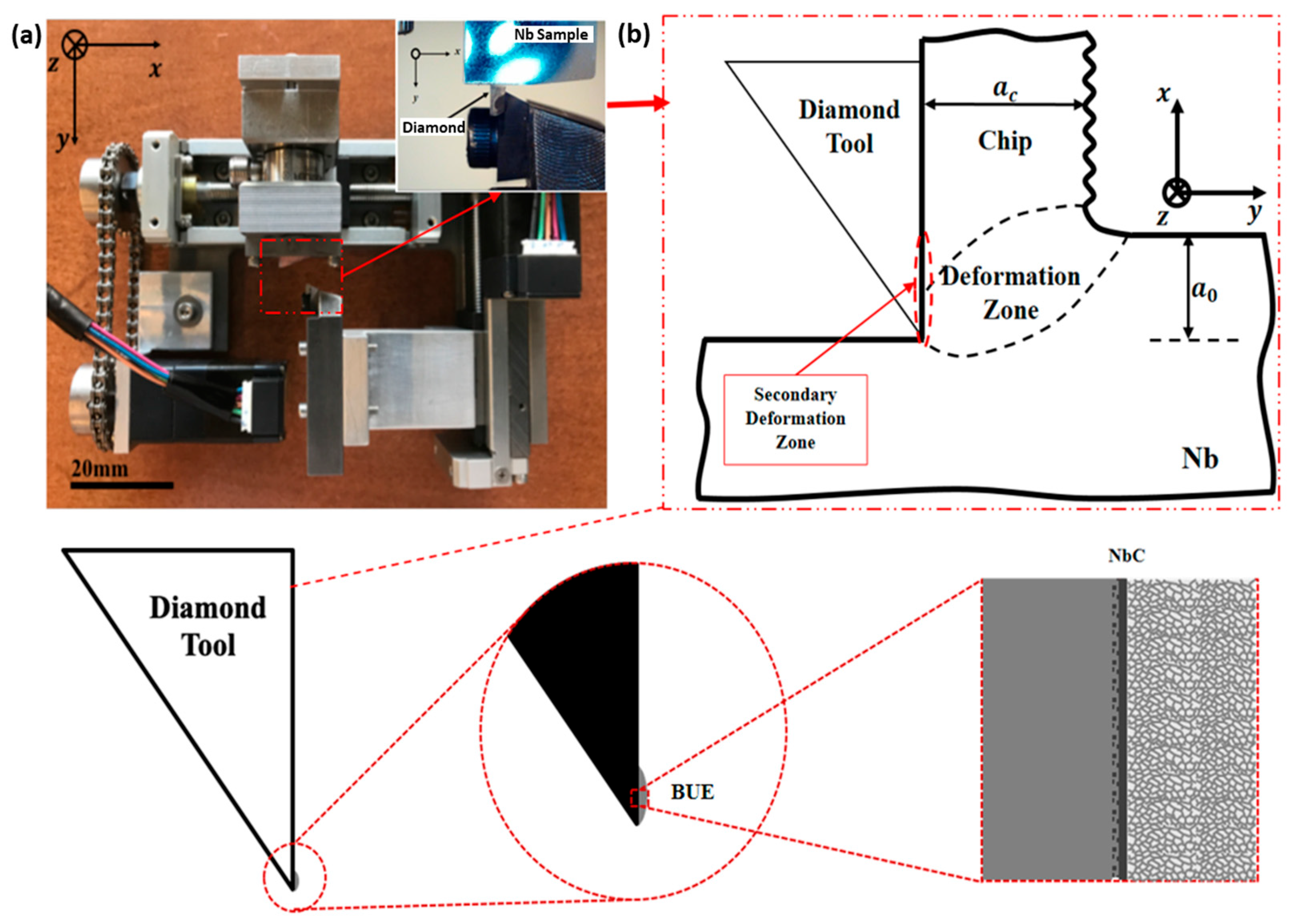
Figure 1a,b illustrate a schematic representation of plane strain machining (PSM) and provide a zoomed-in view of the corresponding sub-stage, where a niobium (Nb) workpiece is mounted. In this configuration, the workpiece moves along the X-axis, while the diamond-cutting tool operates along the Y-axis. The micromachining process is conducted inside a scanning electron microscope (SEM) to enable the high-resolution, in situ observation of deformation phenomena. Under our laboratory conditions, PSM was implemented using a custom-built two-axis deformation stage, which is installed inside the vacuum chamber of an FEI SEM. This specialized micromachining stage was designed and constructed in our lab. The process induces significant localized stresses, and by controlling these stresses, we are able to systematically study the effects of plane strain deformation during micromachining. This setup provides a highly controlled platform to investigate the interaction between cutting mechanics and the material response at the microscale. The area of interest is the secondary shear zone (SSZ), where the diamond rake face contacts the Nb chip. In this zone, the deformation typically measured by its thickness can range from the nanoscale to the microscale, depending on the selected cutting depth (ao ). The rake face contacts the deformed chip, forming the built-up edge (BUE) or what is currently known as the “tribochemical interaction.” This interaction results in NbC layer formation, as illustrated in Figure 1b. During the machining trials, the parameters applied were the machining velocity (V) which remained constant = 150 µm/s, depth of cut (DOC) (ao) = 3 µm, and the travel distance = 700 µm. Niobium’s samples were cut by 10 mm x 10 mm pieces using a diamond saw. After mounting in epoxy, the samples were polished through a conventional metallographic method using abrasive papers with particle sizes of 9, 6, 3, and 1 µm. Final surface finishing was achieved using a 0.04-micrometer colloidal silica suspension to expose the bulk microstructure of niobium. To improve the contrast, the surface was etched with a 1:1 acetic–nitric acid mix for 10–20 s, revealing the Nb microstructure. The average grain size (~100 µm) was significantly larger than the applied cutting depth (ao ≤ 4 µm), yielding an ao/ ac ratio of ~0.5. Although this study was conducted under micromachining conditions, the setup was designed to isolate the fundamental tool–chip interactions at the secondary shear zone. Phenomena such as tribochemical reactions and built-up edge formation are relevant to both micro- and macro-scale machining, even though the scale and thermal environment differ.

3. Results and Discussion

3.1. Deformation Configuration

In situ micromachining was conducted using plane strain machining (PSM), employing a diamond turning on a custom-built two-axis deformation stage inside the FEI /SEM vacuum chamber. The conditions were specifically chosen to limit the thermal effects and to avoid oxidation effects. The relative speed of diamond tool advancement remained consistent at 150 µm/s in most experiments, with the preset cut depth set at 3 µm. Along the z-axis, the workpiece thickness (w) was ≥100 µm and selecting the depth of the cut (ao) to be much smaller than (w) ensured the plane strain condition [24].
By maintaining a constant rake angle at γo = 0°, as shown in Figure 1b, we identified the minimum shear strain, shear, and chip velocities that influence the deformation zones, leading to severe deformation and resulting in recrystallized microstructures and tribochemical interactions of Nb over the diamond tool rake face. Using velocity triangles and angles as guidelines for theoretical calculations, our current objective is to compute the minimum theoretically achievable shear strain. In this specific example, the rake angle (γo) is set to zero, simplifying Equation (1) for shear strain to its most basic form:
ε = c o t β 0 + t a n β 0 γ o = c o t β 0 + t a n β 0
To calculate the minimum shear strain (ε), we started by determining the first- and second-order β 0 differentiations. The first-order derivative must be equal to zero to ensure that the shear strain is either at its minimum or maximum.
First-order differentiation:
d ε d β 0 = d d x 2 s i n 2 β 0
d ε d β 0 = 0 2.2 . cos 2 β o ( s i n 2 β 0 ) 2
d ε d β 0 = 4 cos 2 β 0 ( s i n 2 β 0 ) 2
Second-order differentiation:
d 2 ε d β 0 2 = s i n 2 β 0 2 8 s i n 2 β 0 ( 4 c o s 2 β 0 ) ( 4 c o s 2 β 0 s i n 2 β 0 ) ( s i n 2 β 0 ) 4
d 2 ε d β 0 2 = 8 s i n 2 β 0 2 16 ( c o s 2 β 0 ) 2 ( s i n 2 β 0 ) 3
When the first derivative (dε/dβo) = 0, the solution yields βo = 45. To confirm the minimum shear strain (ε), the second-order derivative ( d 2 ε / d β 0 2 ) at βo = 45° is greater than 0 when plugged into Equation (6). This establishes that the shear strain (ε) reaches its minimum at a shear angle of β 0 = 45°, with a zero orthogonal rake angle of the cutting tool. The calculated value of this minimum shear strain (εmin) was two.
From the generalized expression of the velocity triangle, the following explanation can be expressed as Equation (7). Since the cut speed remained constant at 150 µm/s, the minimum shear velocity was 212 µm/s. Additionally, since a0 = 3 µm and ac ≥ 5 µm, the chip velocity can be calculated via Equation (8) and determined at 90 µm/s.
V c s i n ( 90 + γ o   β o ) = V s s i n ( 90   γ o )
V 0 = a o   V c a c
Theoretically, these calculated values mark the starting point of deformation thresholds. Interestingly, carbide and diamond tools exhibit the ability to react with transition metals at low speeds, forming a built-up edge (BUE) through tribochemical interactions on the rake face. This behavior contrasts with high-speed steel (HSS) tools, which react differently at low speeds. These findings align with the literature, provided that the tool material has no impact on the cutting speed [24]. However, this does not mean that decreased cutting speeds will form the BUE; in fact, it may have no shear strain effect on the rake face. During plastic deformation, most experimental processes result in heat emissions, with over 90% of the energy converted into thermal energy. In high-strain-rate deformations like in situ micromachining, the generated heat might not dissipate effectively within the workpiece. Therefore, machining is a process that involves both thermal and mechanical deformation, where heat effects can further influence the resulting microstructure development. A previous study [24] examined the temperature rise on a large scale (100 µm) using an infrared camera and various milling settings. However, in this study, the deformation configuration posed challenges for direct thermometry in the deformation zone due to spatial restrictions. Therefore, a theoretical estimate of the temperature rise is essential for analyzing the heat effects during in situ micromachining operations. Given the localized nature of plastic deformation, which is concentrated within a limited zone (as described earlier), it can be considered a problem involving a moving source of heat. In this case, the calculations using methods like those described in previous studies [24,25,26] would be a salutation. If ρ = 8.5 g/cm3 and C p = 0.26 J/(gK) represent the density and the specific heat for Nb, respectively, the rise in temperature within the deformation zone can be represented as:
ρ C p T = 1 β × τ × ε
And the amount of heat transferred to the bulk is expressed as:
β = 1 α e r f α + 1 + α e r f c α e α π 1 α ( 1 2 α + α )
where
α = 1 4 V × a o × tan φ  
and κ = 0.24 × 10 4 m2/s is the thermal diffusivity. Based on these calculations, the estimated temperature is under 10 K [21]. The selected machining parameters in this study were designed to maintain isothermal deformation conditions.

3.2. Surface Integrity

Using scanning electron microscopy (SEM), Figure 2a,b depict the condition of the diamond rake face before and after machining, illustrating the influence of cutting conditions on the tribochemical interaction zone. The SEM images reveal the presence of layered reactive bodies within the built-up edge (BUE) structure [27]. Figure 2a shows the pristine diamond rake face before machining, confirming the high surface quality of the cutting tool, comparable to standard requirements for ultra-precision tools. In contrast, Figure 2b captures the rake face after machining niobium (Nb) workpieces and the material transfer and reactivity of Nb with the diamond surface under stress applied through PSM. These images were acquired in situ inside the SEM chamber under isothermal conditions, with live imaging conducted during machining. The BUE is shown to form as Nb chips flow over the diamond rake face, particularly concentrated in SSZ. An intimately bonded BUE forms on the surface of a single-crystal diamond tool, aligning with a common industrial observation in which diamonds experience rapid wear when machining materials like Nb. This results in an extremely poor surface integrity for both the tool and workpiece. A completely new shear surface is formed when a region of an intense stress concentration reaches and extends the outward BUE face. The BUE typically develops downward as it advances forward, causing a cut on the finished surface [28]. To confirm the presence of a built-up edge (BUE) on the cutting tool surface, a diamond-cutting tool was examined via ultrasonic cleaning using an acetone solution after machining. This process aimed to remove any loosely adhered Nb-based deposits before TEM characterization. The purpose of this process was to distinguish between firmly bonded interfacial NbC structures and surface contaminants or mechanically attached Nb layers resulting from the cutting process. This rapid degradation of the diamond-cutting tool is widely observed in the machining of transition metals such as Nb. The experimental deformation configuration choice in this work excludes two previously assumed contributing factors: (a) the ultra-high vacuum environment of the SEM chamber, which almost eliminates any potential interaction with oxygen, and (b) the negligible associated temperature rise with a low machining speed. The roughness was measured via AFM before and after machining to confirm the built-up edge (BUE) effect on the diamond rake face, as depicted in Figure 2c,d. The presence of the BUE significantly compromises the reliability of the finishing surface of the workpiece and shortens the cutting tool’s lifespan. The roughness before machining for the diamond rake face was approximately 6 nm, and the rake face roughness after machining increased to approximately 19 nm. While there is only a small difference before and after the machining experiment, at the nanoscale, there exists a relationship between the roughness and the fraction of the contact face of the cutting tools and workpiece.

3.3. Characterization of the Underlying Deformation and the Element Concentration Profiles Across the Interface

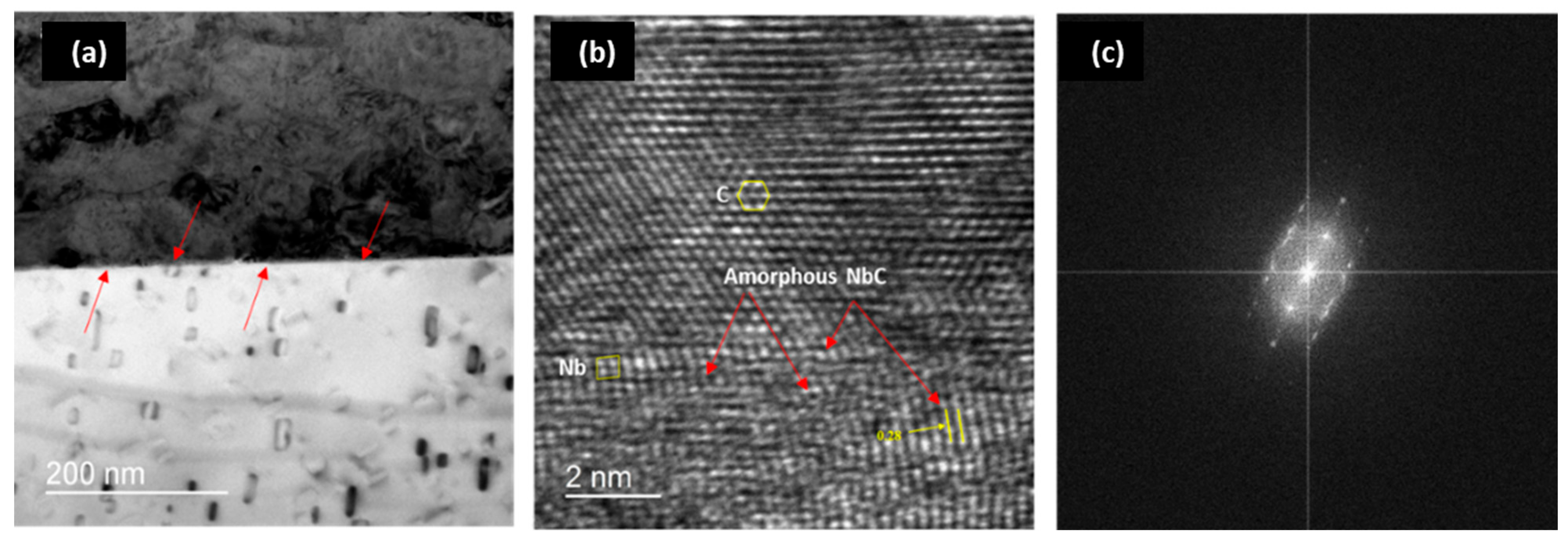
In efforts to reveal the underlying physics for surface defects in diamond-cutting tools, samples for TEM were prepared to observe the featured small specimens using an ultra-high-resolution analytical DualBeam FEI Scios. The examination performed utilized high-resolution TEM to identify carbide formation via TEM (JEOL JEM-2100F XEDS characterization). The initial results show a direct interaction between nanocrystalline Nb and C under mechanical loading, and the observed inter-diffusion is shown in Figure 3a,b. The magnified TEM images showed that no voids or fractures were observed at the interface. The diffusion line is smooth in most regions of the bonding interface, indicating that the surface atoms had directly bonded and reacted with each other to form NbC; this line is marked with red arrows in Figure 3a. The area marked with red arrows represents NbC, and its amorphous lattice planes are depicted in the high-quality resolution TEM image of the diffusion zone shown in Figure 3b. The regions that are likely rich with Nb and C elements have dispersed lattices with different orientations. The high-quality resolution imaging of the lattice exposes a crystalline structure with an interlinear spacing of 0.26 nm. The diffraction orientation of NbC was absorbed; Figure 3c shows the optical diffractograms (fast Fourier transforms of the images) and a light circle that could represent the amorphous structure of NbC, which aligns with previous works [29,30]. The amorphous nature of the NbC layer was confirmed by the absence of lattice fringes in HRTEM and diffuse SAED rings, supported by EDS evidence of Nb–C interdiffusion across a ~20 nm interface. These findings are consistent with prior studies on mechanically induced amorphization in transition metal carbides [31]. However, due to the scarcity of detailed studies on amorphous NbC formation driven purely by the mechanical load, this phenomenon remains an active topic of investigation.
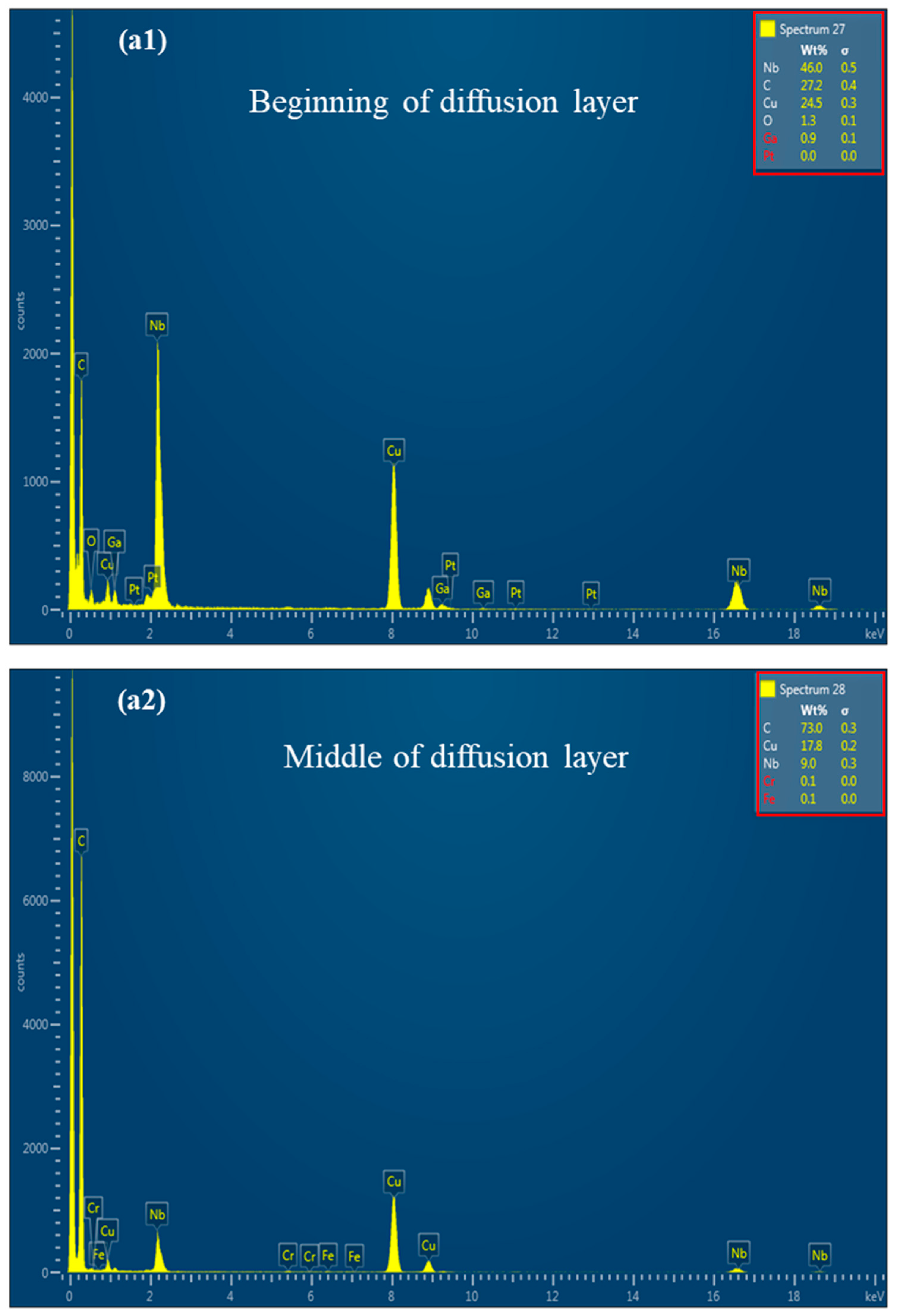
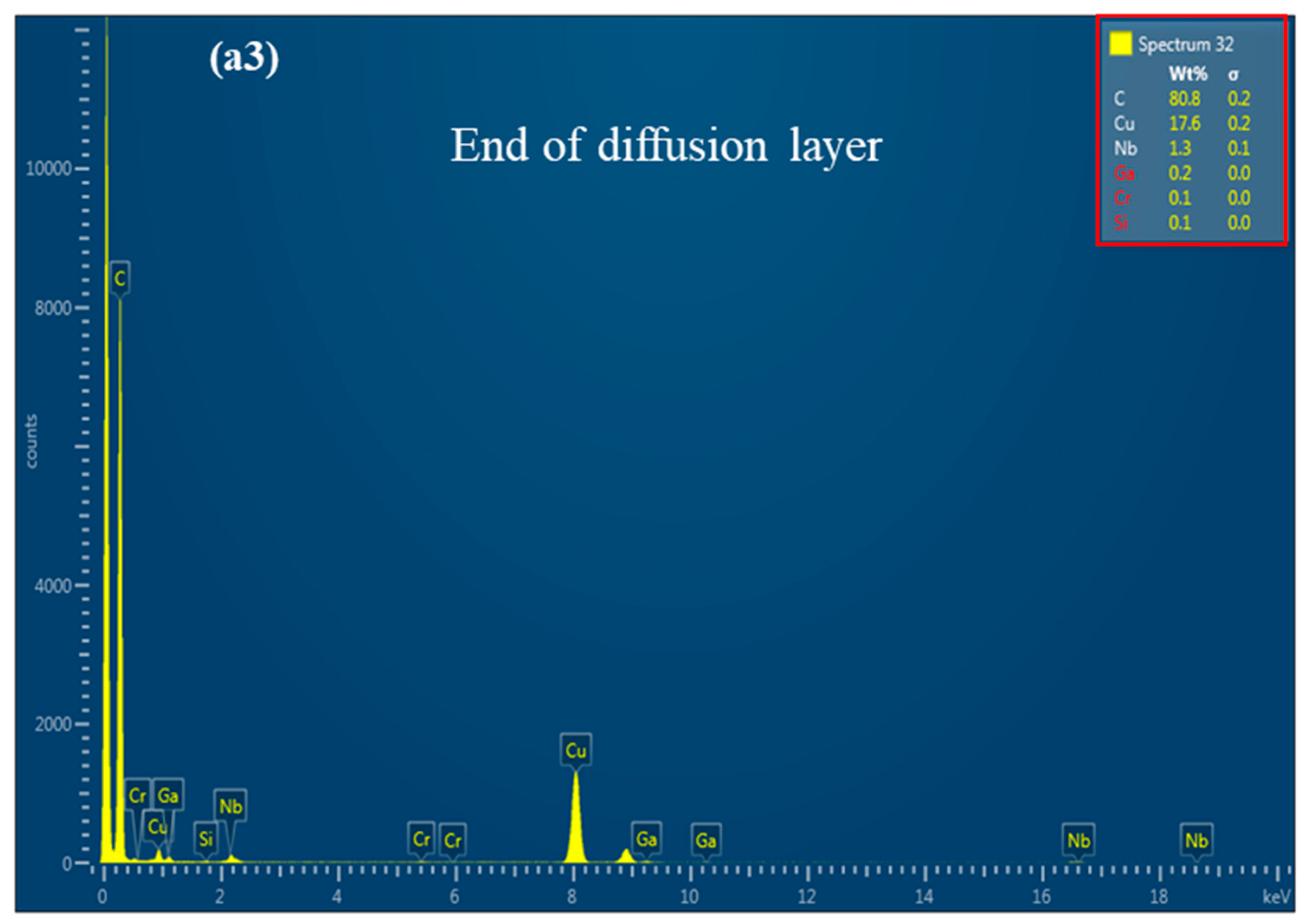
(TEM/EDS) was performed to determine the elemental concentration profiles across the interface. Figure 4 shows the TEM and EDS results. Minimal NbC is found in the mixing layer, as shown in Figure 4a. The distribution of NbC is more prevalent in the Nb side, as shown in the zoomed-in image in Figure 4b. Moreover, the layer spacing is about ~20 nm, determined via EDS line scanning, as shown in Figure 4c. The chemical composition was mapped across the diffusion layer in a “point-by-point” method, as shown in Figure 5. The chemical composition ratio varies from 46% Nb:37% C to 73% Nb:9% C in the middle of the diffusion layer, ultimately increasing to 1.4% Nb:80% C at the end of the diffusion zone. A diffusion layer can form by stacking diamonds on Nb; additionally, a strength between Nb and diamond may be achieved, and NbC can form at the contact area, causing diffusion. More precisely, inter-solid interactions may have resulted in NbC formation. This indicated that the chemical potential of diffusion across interfaces between complex polycrystal formations is linked to applied external and internal stress induced by point defects, dislocations, grain boundaries, triple junctions, and other factors. The assumption is that the atoms migrated due to an element concentration gradient, which can be described as atoms jumping from one adsorption to the next, enhanced under a mechanical load. Also, the known Nb electronic shell structure is elucidated in (2, 8, 18, 12, 1): the fifth energy level contains one unpaired electron. The C electronic shell structure is elucidated in (2, 4): the second energy level carries four paired electrons. Thus, the electrons reacted to form NbC under ideal mechanical loads. Moreover, the tribochemical formation of NbC at the tool–chip interface occurs due to niobium’s strong carbon affinity under high contact stresses [7]. This behavior differs from that observed with non-carbide-forming metals like aluminum, where diamond tools typically remain chemically unaffected.

4. Conclusions

This study outlined the effects of the mechanical load and dynamic tribological systems, performed via orthogonal machining, on the mass transport of single-crystal diamonds with 99.8% pure niobium interfaces. We examined and evaluated the diffusion layer structure under isothermal conditions. The diamond responds to stresses at the rake face produced via micromachining and the resulting tribochemical wear. Both the DOC and cut speed significantly influence stress control in PSM experiments in situ, observed using SEM. The TEM/ESD characterization of microstructures at the interaction layer between monocrystalline Nb and diamond confirmed NbC formation during micromachining, which is attributed to purely mechanical factors that cause diffusion layer formation at the interface.
The strain generated from the vertical movement of the diamond tool to the Nb chip that flows horizontally over the diamond rake face generated significant shear stresses, known as primary shear stress, on the primary shear zone where the chip formed. The second shear stress, known as secondary shear, occurred on the zone where tribochemical wear forms the built-up edge. These large stresses can lead to substantial changes in coarse-grained Nb until ultrafine and nanostructured grains form over the diamond-cutting tool rake face. To reduce the risk of BUE formation, options such as increasing the cutting speed, using inert atmospheres, applying surface treatments to the tool, or employing interrupted cutting may be considered, depending on the specific machining setup.

Author Contributions

Conceptualization, M.R.S. and M.S.A.; methodology, M.S.A.; formal analysis, M.S.A.; investigation, M.S.A., M.T.A. and R.A.A.; resources, M.R.S.; data curation, M.S.A., M.T.A. and R.A.A.; writing—original draft preparation, M.S.A., M.T.A. and R.A.A.; writing—review and editing, M.T.A. and R.A.A.; supervision, M.R.S.; funding acquisition, M.R.S. All authors have read and agreed to the published version of the manuscript.

Funding

This research was partially funded by II–VI Foundation Block Gift Program.

Data Availability Statement

Data available upon request.

Acknowledgments

This paper is based on the Doctoral Dissertation by M.S.A., which acknowledges support from the II–VI Foundation Block Gift Program. M.S.A., M.T.A., and R.A.A. would also like to extend their appreciation to King Abdulaziz City for Science and Technology (KACST) for their financial support. All authors have reviewed and approved the acknowledgements section and consent to the inclusion of the individuals named.

Conflicts of Interest

The authors declare no conflict of interest.

Nomenclature

a 0 depth of cut
Ddiffusion coeffiecient
E a P activation energy
Jdiffusion flux
κ thermal diffusivity
Rgas constant
Ttemperature
Vmachining velocity
Vcchip velocity
wworkpeice thickness
εshear strain
γorack angle
β 0 shear angle

References

  1. Schey, J.A. Introduction to Manufacturing Processes; McGraw-Hill: New York, NY, USA, 1987; Volume 2. [Google Scholar]
  2. Schulz, H.; Moriwaki, T. High-speed Machining. CIRP Ann. 1992, 41, 637–643. [Google Scholar] [CrossRef]
  3. Artini, C.; Muolo, M.L.; Passerone, A. Diamond–metal interfaces in cutting tools: A review. J. Mater. Sci. 2012, 47, 3252–3264. [Google Scholar] [CrossRef]
  4. Zou, L.; Yin, J.; Huang, Y.; Zhou, M. Essential causes for tool wear of single crystal diamond in ultra-precision cutting of ferrous metals. Diam. Relat. Mater. 2018, 86, 29–40. [Google Scholar] [CrossRef]
  5. Abolghasem, S.; Basu, S.; Shekhar, S.; Cai, J.; Shankar, M.R. Mapping subgrain sizes resulting from severe simple shear deformation. Acta Mater. 2012, 60, 376–386. [Google Scholar] [CrossRef]
  6. Tomac, N.; Tønnessen, K.; Rasch, F.O.; Mikac, T. A study of factors that affect the build-up material formation. In AMST’05 Advanced Manufacturing Systems and Technology: Proceedings of the Seventh International Conference; Springer: Vienna, Austria, 2005; pp. 183–192. [Google Scholar]
  7. Paul, E.; Evans, C.J.; Mangamelli, A.; McGlauflin, M.L.; Polvani, R.S. Chemical aspects of tool wear in single point diamond turning. Precis. Eng. 1996, 18, 4–19. [Google Scholar] [CrossRef]
  8. Qu, J.; Blau, P.J.; Watkins, T.R.; Cavin, O.B.; Kulkarni, N.S. Friction and wear of titanium alloys sliding against metal, polymer, and ceramic counterfaces. Wear 2005, 258, 1348–1356. [Google Scholar] [CrossRef]
  9. Kumar, B.; Kumar, D.; Chaudhry, V. Tribological behavior of zirconium alloy against stainless steel under different conditions. Tribol. Int. 2023, 189, 108995. [Google Scholar] [CrossRef]
  10. Murakami, T.; Mano, H.; Kaneda, K.; Hata, M.; Sasaki, S.; Sugimura, J. Friction and wear properties of zirconium and niobium in a hydrogen environment. Wear 2010, 268, 721–729. [Google Scholar] [CrossRef]
  11. Bayer, R.G. Mechanical Wear Prediction and Prevention; Marcel Dekker: New York, NY, USA, 1994; p. 280. [Google Scholar]
  12. Kozasu, I.; Ouchi, C.; Sampei, T.; Okita, T. Hot rolling as a high-temperature thermo-mechanical process. In Proceedings of the Conference on Microalloying 75; Union Carbide Corp.: New York, NY, USA, 1977; pp. 120–135. [Google Scholar]
  13. Burwell, J.T. Survey of possible wear mechanisms. Wear 1957, 1, 119–141. [Google Scholar] [CrossRef]
  14. Zhang, S.; To, S.; Zhang, G. Diamond tool wear in ultra-precision machining. Int. J. Adv. Manuf. Technol. 2017, 88, 613–641. [Google Scholar] [CrossRef]
  15. Cheng, P.; Jiang, N.; Wu, Z. Effect of nickel element diffusion on the tribological properties of cemented carbide materials under high temperature condition. J. Mater. Eng. Perform. 2025, 34, 2788–2799. [Google Scholar] [CrossRef]
  16. Krishnaraj, N.; Roy, M. Tribology of Diffusion-Treated Surfaces. In Surface Engineering for Enhanced Performance Against Wear; Springer: Vienna, Austria, 2013; pp. 111–147. [Google Scholar]
  17. Gekonde, H.O.; Subramanian, S.V. Tribology of tool–chip interface and tool wear mechanisms. Surf. Coat. Technol. 2002, 149, 151–160. [Google Scholar] [CrossRef]
  18. Mehrer, H. Continuum theory of diffusion. In Diffusion in Solids: Fundamentals, Methods, Materials, Diffusion-Controlled Processes; Springer: Berlin/Heidelberg, Germany, 2007; pp. 27–36. [Google Scholar]
  19. Goswami, T.K.; Mangaraj, S. 8—Advances in polymeric materials for modifie atmosphere packaging (MAP). In Multifunctional and Nanoreinforced Polymers for Food Packaging; Lagarón, J.-M., Ed.; Woodhead Publishing: Sawston, UK, 2011; pp. 163–242. [Google Scholar]
  20. Moghadam, M.M.; Rickman, J.M.; Harmer, M.P.; Chan, H.M. The role of boundary variability in polycrystalline grain-boundary diffusion. J. Appl. Phys. 2015, 117, 045311. [Google Scholar] [CrossRef]
  21. Cahn, R.W.; Haasen, P. (Eds.) Physical Metallurgy; Elsevier: Amsterdam, The Netherlands, 1996; Volume 1. [Google Scholar]
  22. Shang, S.-L.; Zhou, B.-C.; Wang, W.Y.; Ross, A.J.; Liu, X.L.; Hu, Y.-J.; Fang, H.-Z.; Wang, Y.; Liu, Z.-K. A comprehensive first-principles study of pure elements: Vacancy formation and migration energies and self-diffusion coefficients. Acta Mater. 2016, 109, 128–141. [Google Scholar] [CrossRef]
  23. Bilbao, L.; Ortueta, M.; Mijangos, F. Effect of concentration and temperature on mass transfer in metal ion exchange. Ind. Eng. Chem. Res. 2016, 55, 7287–7295. [Google Scholar] [CrossRef]
  24. Gong, S.; Ravi Shankar, M. Effect of microstructural anisotropy on severe plastic deformation during material removal at micrometer length-scales. Mater. Des. 2020, 194, 108874. [Google Scholar] [CrossRef]
  25. Basu, S.; Shankar, M.R. Microstructure evolution during severe shea deformation at small length-scales. Scr. Mater. 2014, 72, 51–54. [Google Scholar] [CrossRef]
  26. Basu, S.; Shankar, M.R. Spatial connement-induced switchover in microstructure evolution during severe plastic deformation at micrometer length scales. Acta Mater. 2014, 79, 146–158. [Google Scholar] [CrossRef]
  27. Shaw, M.C.; Sanghani, S.R. Cutting characteristics with variable undeformed chip thickness. CIRP Ann. 1963, 10, 240. [Google Scholar]
  28. Shaw, M.C.; Cookson, J.O. Metal Cutting Principles; Oxford University Press: New York, NY, USA, 2005. [Google Scholar]
  29. Zhong, L.; Wei, J.; Bai, H.; Zhu, J.; Xu, Y. Effects of soaking time on the microstructure and mechanical properties of Nb-NbC/Fe core–shell rod-reinforced cast-iron-matrix composite fabricated through two-step in situ solid-phase diffusion. J. Mater. Res. Technol. 2020, 9, 12308–12317. [Google Scholar] [CrossRef]
  30. Almeida, A.; Eugénio, S.; Livramento, V.; Marques, M.T.; Correia, J.B.; Vilar, R. Laser cladding of Cu-NbC nanocomposite coatings. In International Congress on Applications of Lasers & Electro-Optics; Laser Institute of America: Orlando, FL, USA, 2006; Volume 2006. [Google Scholar]
  31. Tengstrand, O.; Nedfors, N.; Andersson, M.; Lu, J.; Jansson, U.; Flink, A.; Eklund, P.; Hultman, L. Model for electron-beam-induced crystallization of amorphous Me–Si–C (Me= Nb or Zr) thin films. J. Mater. Res. 2014, 29, 2854–2862. [Google Scholar] [CrossRef]
Figure 1. (a) Photo of high-speed machining station and zoomed-in image of diamond-cutting tool with Nb. (b) Schematic plot of high-speed micro-/nano-machining station and schematic of BUE and expected NbC layer in the TEM sample.
Jmmp 09 00176 g001
Figure 2. (a) SEM image of the rake face of diamond-cutting tool before micromachining experiments. (b) SEM image of the rake face of diamond-cutting tool after micromachining experiments in situ, ao = 3 μm and V = 150 μm/s. (c) The diamond rake face roughness before machining. (d) The diamond rake face roughness after machining via AFM.
Jmmp 09 00176 g002
Figure 3. (a) TEM bright-field images of cross-sectional diffusion layers. (b) Highly magnified TEM image at diffusion area that shows lattice orientation. (c) Lattice diffraction at NbC diffusion layer.
Jmmp 09 00176 g003
Figure 4. TEM bright-field images of cross-sectional diffusion layers: (a) in situ PSM ao = 3 μm and V = 150 μm/s; (b) zoomed-in view corresponding to the rectangle shows C and Nb detected on diffusion layer. (c) EDS mapping through diffusion layer shows change in C and Nb concentrations at interface.
Jmmp 09 00176 g004
Figure 5. EDS mapping through diffusion layer shows change in C and Nb concentrations at the (a1) beginning, (a2) middle, and (a3) end of the layer.
Jmmp 09 00176 g005aJmmp 09 00176 g005b
Disclaimer/Publisher’s Note: The statements, opinions and data contained in all publications are solely those of the individual author(s) and contributor(s) and not of MDPI and/or the editor(s). MDPI and/or the editor(s) disclaim responsibility for any injury to people or property resulting from any ideas, methods, instructions or products referred to in the content.