
Recent Applications of Focused Ion Beam–Scanning Electron Microscopy in Advanced Packaging


Abstract
1. Introduction
2. Evolution of Advanced Packaging Technologies and Characterization Challenges
3. Core Applications of FIB-SEM in Advanced Packaging
3.1. Optimization of TSV/TGV Processes
3.2. The Reliability Assessment of the Process
3.3. Research on RDL Failure Mechanisms
4. Innovation in Multimodal Integration Technology
4.1. XRM-FIB 3D Navigation System
4.2. EBSD-FIB Crystallographic Analysis
4.3. FIB-TOFS In Situ Imaging
5. Summary and Prospects
Author Contributions
Funding
Data Availability Statement
Conflicts of Interest
References
- Chen, Z.; Zhang, J.; Wang, S.; Wong, C.-P. Challenges and prospects for advanced packaging. Fundam. Res. 2024, 4, 1445–1458. [Google Scholar] [CrossRef] [PubMed]
- Lau, J.H. Recent Advances and Trends in Advanced Packaging. IEEE Trans. Components Packag. Manuf. Technol. 2022, 12, 228–252. [Google Scholar] [CrossRef]
- Chaware, R.; Hariharan, G.; Lin, J.; Singh, I.; O’Rourke, G.; Ng, K. Assembly Challenges in Developing 3D IC Package with Ultra High Yield and High Reliability. In Proceedings of the 2015 IEEE 65th Electronic Components and Technology Conference (ECTC), San Diego, CA, USA, 26–29 May 2015; pp. 1447–1451. [Google Scholar]
- Khan, N.; Yu, L.H.; Pin, T.S.; Ho, S.W.; Kripesh, V.; Pinjala, D. 3-D Packaging With Through-Silicon Via (TSV) for Electrical and Fluidic Interconnections. IEEE Trans. Components Packag. Manuf. Technol. 2013, 3, 221–228. [Google Scholar] [CrossRef]
- Knickerbocker, J.U.; Patel, C.S.; Andry, P.S.; Tsang, C.K.; Buchwalter, L.P.; Sprogis, E.J. 3-D Silicon Integration and Silicon Packaging Technology Using Silicon Through-Vias. IEEE J. Solid-State Circuits 2006, 41, 1718–1725. [Google Scholar] [CrossRef]
- Duan, G.; Kanaoka, Y.; McRee, R.; Nie, B.; Manepalli, R. Die Embedding Challenges for EMIB Advanced Packaging Technology. In Proceedings of the 2021 IEEE 71st Electronic Components and Technology Conference (ECTC), San Diego, CA, USA, 1 June–4 July 2021; pp. 1–7. [Google Scholar]
- Lau, J.H. Recent advances and trends in heterogeneous integrations. J. Microelectron. Electron. Packag. 2019, 16, 45–77. [Google Scholar] [CrossRef]
- Ma, X.; Wang, Y.; Wang, Y.; Cai, X.; Han, Y. Survey on chiplets: Interface, interconnect and integration methodology. CCF Trans. High Perform. Comput. 2022, 4, 43–52. [Google Scholar] [CrossRef]
- Agrawal, Y.; Mummaneni, K.; Sathyakam, P.U. Interconnect Technologies for Integrated Circuits and Flexible Electronics; Springer: Singapore, 2024. [Google Scholar]
- Kaestner, M.; Mueller, S.; Gregorich, T.; Hartfield, C.; Nolen, C.; Schulmeyer, I. Novel Workflow for High-Resolution Imaging of Structures in Advanced 3D and Fan-Out Packages. In Proceedings of the 2019 China Semiconductor Technology International Conference (CSTIC), Shanghai, China, 18–19 March 2019; pp. 1–3. [Google Scholar]
- Mohammad, K.N.; Sim, K.S. Novel application of FIB lift-out and ultramicrotomy for advanced package failure analysis. In Proceedings of the 9th International Symposium on the Physical and Failure Analysis of Integrated Circuits, Singapore, 8–12 July 2002; pp. 159–163. [Google Scholar]
- Tang, T.N.; Heng, H.C.; Chan, S.Y.; Hiew, M. Detection of underfill epoxy defects in flip chip packages with the aid of SAM, parallel polishing and FIB. In Proceedings of the 1999 7th International Symposium on the Physical and Failure Analysis of Integrated Circuits, Singapore, 9 July 1999. [Google Scholar]
- Chandrakar, S.; Gupta, D.; Majumder, M.K. Impact of TSV bump and redistribution layer on crosstalk delay and power loss. Mem.—Mater. Devices Circuits Syst. 2023, 4, 100040. [Google Scholar] [CrossRef]
- Pathak, A.; Friedrich, G.; Teutsch, T. Non-Formaldehyde based electroless Cu deposition for Advanced Packaging. In Proceedings of the 2020 IEEE 22nd Electronics Packaging Technology Conference (EPTC), Singapore, 2–4 December 2020. [Google Scholar]
- Kim, M.J.; Lee, S.H.; Suk, K.L.; Jang, J.G.; Jeon, G.-J.; Choi, J.-I. Novel 2.5D RDL Interposer Packaging: A Key Enabler for the New Era of Heterogenous Chip Integration. In Proceedings of the 2021 IEEE 71st Electronic Components and Technology Conference (ECTC), San Diego, CA, USA, 1 June–4 July 2021. [Google Scholar]
- Medhat, D. 2.5/3D IC Reliability Verification Has Come A Long Way. Semiconductor Engineering. Available online: https://semiengineering.com/2-5-3d-ic-reliability-verification-has-come-a-long-way (accessed on 1 August 2022).
- Wesling, P. The heterogeneous integration roadmap: Enabling technology for systems of the future. In Proceedings of the 2020 Pan Pacific Microelectronics Symposium, Kohala Coast, HI, USA, 10–13 February 2020. [Google Scholar]
- Lau, J.H. Overview and outlook of through-silicon via (TSV) and 3D integrations. Microelectron. Int. 2011, 28, 8–22. [Google Scholar] [CrossRef]
- Ingerly, D.B.; Amin, S.; Aryasomayajula, L.; Balankutty, A.; Borst, D.; Chandra, A. Foveros: 3D integration and the use of face-to-face chip stacking for logic devices. In Proceedings of the 2019 IEEE International Electron Devices Meeting, San Francisco, CA, USA, 7–11 December 2019. [Google Scholar]
- Gomes, W.; Khushu, S.; Ingerly, D.B.; Stover, P.N. 8.1 lakefield and mobility compute: A 3D stacked 10 nm and 22FFL hybrid processor system in 12 × 12 mm2, 1 mm package-on-package. In Proceedings of the 2020 IEEE International Solid-State Circuits Conference—(ISSCC), San Francisco, CA, USA, 16–20 February 2020. [Google Scholar]
- Inoue, K.; Fujimura, T.; Takayama, M.; Onitake, S. Direct copper metallization on TGV (Thru-Glass-Via) for high performance glass substrate. In Proceedings of the 2017 21st European Microelectronics and Packaging Conference (EMPC) & Exhibition, Warsaw, Poland, 10–13 September 2017. [Google Scholar]
- Gambino, J.P.; Adderly, S.A.; Knickerbocke, J.U. An overview of through-silicon-via technology and manufacturing challenges. Microelectron. Eng. 2015, 135, 73–106. [Google Scholar] [CrossRef]
- Lai, Z.; Liu, D.; Zhao, T.; Zhang, Y.; Liang, X.; Sun, R. Directly Electroplated Metallization on Through Glass Via (TGV) Using Silver Nanowires Conductive Composite as Seed Layer. In Proceedings of the 2023 24th International Conference on Electronic Packaging Technology (ICEPT), Shihezi City, China, 8–11 August 2023. [Google Scholar]
- Gallois-Garreignot, S.; Benzima, N.; Benmussa, E.; Moutin, C.; Bouchard, P.O.; Fiori, V.; Tavernier, C. Qualification of bumping processes: Experimental and numerical investigations on mechanical stress and failure modes induced by shear test. Microelectron. Reliab. 2015, 55, 980–989. [Google Scholar] [CrossRef]
- Libres, J.; Arroyo, J.C. Investigation of Bump Crack and Deformation on Pb-Free Flip Chip Packages. In Proceedings of the 2010 Proceedings 60th Electronic Components and Technology Conference (ECTC), Las Vegas, NV, USA, 1–4 June 2010. [Google Scholar]
- Nam, S.; Kang, J.; Lee, I.; Kim, Y.; Yu, H.J.; Kim, D.-W. Investigation on Package Warpage and Reliability of the large size 2.5D Molded Interposer on Substrate (MIoS) Package. In Proceedings of the 2022 IEEE 72nd Electronic Components and Technology Conference (ECTC), San Diego, CA, USA, 31 May–3 June 2022. [Google Scholar]
- Jin, S.; Do, W.; Jeong, J.; Cha, H.; Jeong, Y.; Khim, J. Substrate Silicon Wafer Integrated Fan-out Technology (S-SWIFT®) Packaging with Fine Pitch Embedded Trace RDL. In Proceedings of the 2022 IEEE 72nd Electronic Components and Technology Conference (ECTC), San Diego, CA, USA, 31 May–3 June 2022. [Google Scholar]
- Abdullah, M.F.; Lee, H.W. Technology review of CNTs TSV in 3D IC and 2.5D packaging: Progress and challenges from an electrical viewpoint. Microelectron. Eng. 2024, 290, 112189. [Google Scholar] [CrossRef]
- Gambino, J.P.; Doan, T.; Trapasso, J.; Musante, C.; Dang, D.; Vanslette, D. Through-silicon-via Process Control in Manufacturing for SiGe Power Amplifiers. In Proceedings of the 2013 IEEE 63rd Electronic Components and Technology Conference, Las Vegas, NV, USA, 28–31 May 2013. [Google Scholar]
- Dou, H.; Yang, M.; Chen, Y.; Qiao, Y. Analysis of the structure evolution and crack propagation of Cu-Filled TSV after thermal shock test. In Proceedings of the 2017 18th International Conference on Electronic Packaging Technology (ICEPT), Harbin, China, 16–19 August 2017. [Google Scholar]
- Lee, C.-M.; Chen, H.-P.; Chang, Y.-C.; Hsieh, W.-K.; Kao, L.-H. Fluorocarbon Film Deposition Using Reactive Ion Etcher and Its Application for Physical Analysis of 3D Stacking TSV Micro Bump and Hybrid Bonding. In Proceedings of the 2024 IEEE International Symposium on the Physical and Failure Analysis of Integrated Circuits (IPFA), Singapore, 15–18 July 2024. [Google Scholar]
- Ji, L.; Jing, X.; Xue, K.; Xu, C.; He, H.; Zhang, W. Effect of annealing after copper plating on the pumping behavior of through silicon vias. In Proceedings of the 2014 15th International Conference on Electronic Packaging Technology, Chengdu, China, 12–15 August 2014. [Google Scholar]
- Li, Z.; Ma, L.; Zhao, X.; Wang, Y.; Guo, F. Effect of annealing process on microstructure of Cu-TSV. In Proceedings of the 2017 18th International Conference on Electronic Packaging Technology (ICEPT), Harbin, China, 16–19 August 2017. [Google Scholar]
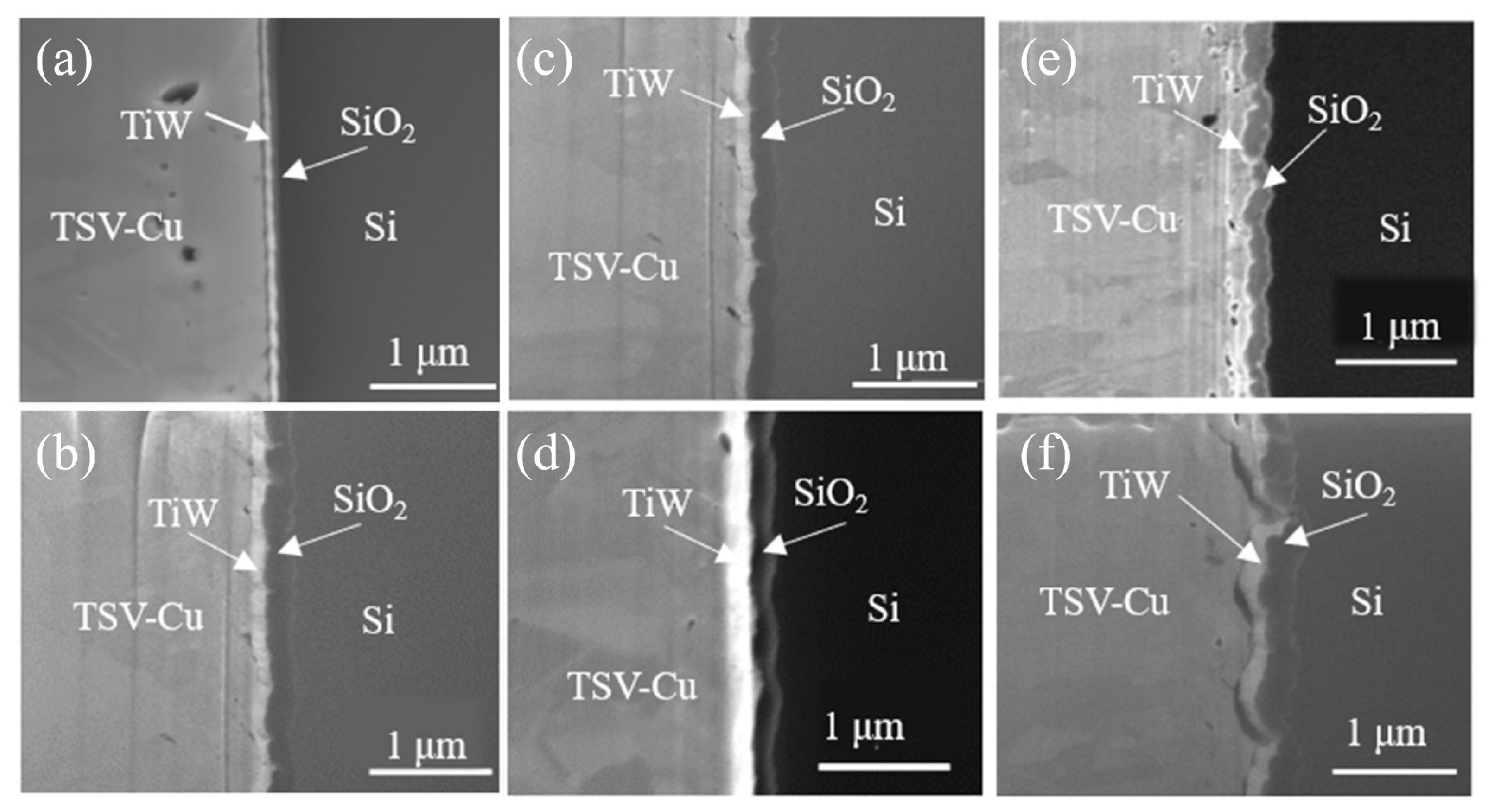
- Zhang, M.; Chen, F.; Qin, F.; Chen, S.; Dai, Y. Correlations between Microstructure and Residual Stress of Nanoscale Depth Profiles for TSV-Cu/TiW/SiO2/Si Interfaces after Different Thermal Loading. Materials 2023, 16, 449. [Google Scholar] [CrossRef]
- Shao, J.; Shi, T.; Du, L.; Su, L.; Lu, X.; Liao, G. Analysis on annealing-induced stress of blind-via TSV using FEM. Front. Mech. Eng. 2018, 13, 401–410. [Google Scholar] [CrossRef]
- Chan, Y.S.; Li, H.Y.; Zhang, X. Thermo-Mechanical Design Rules for the Fabrication of TSV Interposers. IEEE Trans. Components Packag. Manuf. Technol. 2013, 4, 633–640. [Google Scholar] [CrossRef]
- Kong, L.; Rudack, A.C.; Krueger, P.; Zschech, E.; Arkalgud, S.; Diebold, A.C. 3D-interconnect Visualization of extrusion and voids induced in Cu-filled TSVs at various temperature by XRM. Microelectron. Eng. 2012, 92, 24–28. [Google Scholar] [CrossRef]
- Liu, T.; Liu, S.; Hu, X.; Dong, F.; Chen, Z.; Peng, H. Study on the Effect of Film Process on Interface and Interconnection Reliability in the TSV Structure. In Proceedings of the 2024 25th International Conference on Electronic Packaging Technology (ICEPT), Tianjin, China, 7–9 August 2024. [Google Scholar]
- Beyne, E. Reliable Via-Middle Copper Through-Silicon Via Technology for 3-D Integration. IEEE Trans. Components Packag. Manuf. Technol. 2016, 6, 983–992. [Google Scholar] [CrossRef]
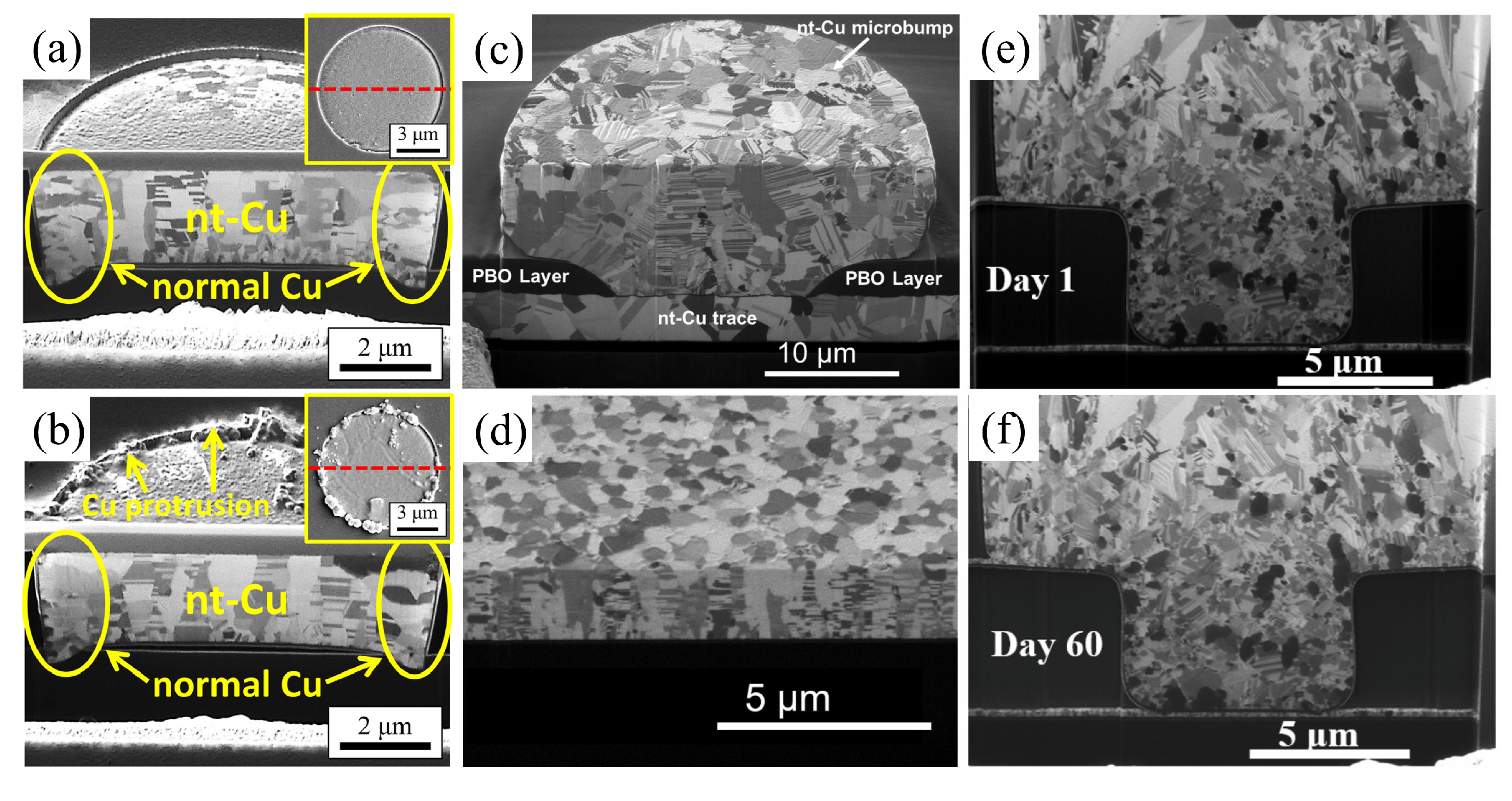
- Zheng, Z.; Huang, Y.-T.; Wang, Z.; Zhang, M.; Wang, W.-T.; Chung, C.-C.; Cherng, S.-J.; Tsai, Y.-H.; Li, P.-C.; Lu, Z.; et al. Electrodeposition of (111)-oriented and nanotwin-doped nanocrystalline Cu with ultrahigh strength for 3D IC application. Nanotechnology 2021, 32, 225702. [Google Scholar] [CrossRef]
- Lin, C.-C.; Hu, C.-C. The Ultrahigh-Rate Growth of Nanotwinned Copper Induced by Thiol Organic Additives. J. Electrochem. Soc. 2020, 167, 082505. [Google Scholar] [CrossRef]
- Lin, T.C.; Liang, C.L.; Wang, S.B.; Lin, Y.S.; Kao, C.L.; Tarng, D.; Lin, K.L. Inhibiting the detrimental Cu protrusion in Cu through-silicon-via by highly (111)-oriented nanotwinned Cu. Scr. Mater. 2021, 197, 113782. [Google Scholar] [CrossRef]
- Kuo, Y.-H.; Tran, D.-P.; Ong, J.-J.; Tu, K.N.; Chen, C. Hybrid Cu-to-Cu bonding with nano-twinned Cu and non-conductive paste. J. Mater. Res. Technol. 2022, 18, 859–871. [Google Scholar] [CrossRef]
- Chen, C.; Cherng, S.-J.; He, C.; Chung, C.-C.; Wang, S.; Huang, Y.-T.; Feng, S.P. Nanotwinning-assisted structurally stable copper for fine-pitch redistribution layer in 2.5D/3D IC packaging. J. Mater. Res. Technol. 2023, 27, 4883–4890. [Google Scholar] [CrossRef]
- Pan, K.; Xu, J.; Lai, Y.; Park, S.; Okoro, C.; Joshi, D. Investigation of Copper and Glass Interaction in Through Glass Via (TGV) During Thermal Cycling. In Proceedings of the 2021 IEEE 71st Electronic Components and Technology Conference (ECTC), San Diego, CA, USA, 1 June–4 July 2021. [Google Scholar]
- Shorey, A.; Pollard, S.; Streltsov, A.; Piech, G.; Wagner, R. Development of substrates for through glass vias (TGV) for 3DS-IC integration. In Proceedings of the 2012 IEEE 62nd Electronic Components and Technology Conference, San Diego, CA, USA, 29 May–1 June 2012. [Google Scholar]
- Lu, Y.; Wang, J. Thermo-mechanical Reliability of Micro-joints in a RF Packaging with Through Glass Via (TGV) Interposer. In Proceedings of the 2024 25th International Conference on Electronic Packaging Technology (ICEPT), Tianjin, China, 7–9 August 2024. [Google Scholar]
- Chang, Y.-H.; Tseng, P.-L.; Lin, J.-C.; Chen, J.-C.; Huang, M.-C.; Lin, H.-Y.; Pollard, S.; Mazumder, P. Communication-defect-free filling of high aspect ratio through vias in ultrathin glass. J. Electrochem. Soc. 2019, 166, D3155. [Google Scholar] [CrossRef]
- Ogutu, P.; Fey, E.; Dimitrov, N. Superconformal Filling of High Aspect Ratio through Glass Vias (TGV) for Interposer Applications Using TNBT and NTBC Additives. J. Electrochem. Soc. 2015, 162, D457. [Google Scholar] [CrossRef]
- Han, S.; Chang, P.; Zhou, Z.; Wu, Y.; Li, M.; Hang, T. Effect of intermolecular and intramolecular synergism on the inhibition from hybrid additives in damascene copper electrodeposition. Electrochim. Acta 2024, 483, 144001. [Google Scholar] [CrossRef]
- Hai, N.T.M.; Broekmann, P. Smart Hybrid Polymers for Advanced Damascene Electroplating: Combination of Superfill and Leveling Properties. Fundam. Res. 2015, 2, 1096–1099. [Google Scholar] [CrossRef]
- Chen, Z.; Zhang, J.; Wang, S.; Wong, C.-P. Synergistic Effect of Additives on Filling of Tapered TGV vias by copper electroplating. ChemElectroChem 2024, 4, 1445–1458. [Google Scholar]
- Yang, G.; Li, L.; Chang, L.; Yang, W.; Zhang, G.; Zhang, Z. Residual Stress Control Based on Electroplated Metal grain chracteristics in panel-level glass advanced packaging. In Proceedings of the 2024 25th International Conference on Electronic Packaging Technology (ICEPT), Tianjin, China, 7–9 August 2024. [Google Scholar]
- Lau, J.H. Recent Advances and Trends in Cu–Cu Hybrid Bonding. IEEE Trans. Components Packag. Manuf. Technol. 2023, 13, 399–425. [Google Scholar] [CrossRef]
- Nicolas, S.; Suarez-Berru, J.-J.; Bresson, N.; Socquet-Clerc, C.; Assous, M.; Borel, S. 3-layer Fine Pitch Cu-Cu Hybrid Bonding Demonstrator With High Density TSV For Advanced CMOS Image Sensor Applications. In Proceedings of the 2024 IEEE 74th Electronic Components and Technology Conference (ECTC), Denver, CO, USA, 28–31 May 2024. [Google Scholar]
- Lee, T.-k.; Yang, H.; Dutta, I. Damage Mechanisms in Through-Silicon Vias Due to Thermal Exposure. J. Electron. Mater. 2024, 53, 1214–1222. [Google Scholar] [CrossRef]
- Pearson, R.A.; Oldak, R. Predicting the strength of underfill/polyimide interfaces. In Proceedings of the 9th International Symposium on Advanced Packaging Materials: Processes, Properties and Interfaces (IEEE Cat. No.04TH8742). 2004 Proceedings, Atlanta, GA, USA, 24–26 March 2004. [Google Scholar]
- Shi, L.; Chen, L.; Zhang, D.W.; Liu, E.; Huang, J.-X. Investigation on Solder Bump Process Polyimide Cracking for wafer level packaging. In Proceedings of the 2016 17th International Conference on Electronic Packaging Technology (ICEPT), Wuhan, China, 16–19 August 2016. [Google Scholar]
- De Haven, K.; Dietz, J. Controlled Collapse Chip Connection (C4)—An Enabling Technology. In Proceedings of the 1994 Proceedings. 44th Electronic Components and Technology Conference, Washington, DC, USA, 1–4 May 1994. [Google Scholar]
- Yu, J.; Anand, A.; Mui, Y.C.; Srinivasan, P.; Master, R. Reliability Study on Copper Pillar Bumping with Lead Free Solder. In Proceedings of the 2007 9th Electronics Packaging Technology Conference, Singapore, 7–9 December 2008. [Google Scholar]
- Taneja, D.; Danovitch, D.; Chakroun, A.; Dufort, C.; Gagnon, P.; Martel, R. Thermal Compression Bonding with Pre-Applied Underfill for Very Large Die. In Proceedings of the 2020 IEEE 70th Electronic Components and Technology Conference (ECTC), Orlando, FL, USA, 1–4 June 2020. [Google Scholar]
- Lim, A.B.Y.; Rezvani, A.; Bacay, R.D.; Colosimo, T.; Yauw, O.; Clauberg, H. High throughput thermo-compression bonding with pre-applied underfill for 3D memory applications. In Proceedings of the 2016 IEEE 18th Electronics Packaging Technology Conference (EPTC), Singapore, 30 November–3 December 2016. [Google Scholar]
- Ito, M.; Kato, J.; Nonaka, T. 3D Analysis of Flip Chip Interconnection using FIB-SEM Slice and View. In Proceedings of the 2015 International Conference on Electronics Packaging and iMAPS All Asia Conference (ICEP-IAAC), Kyoto, Japan, 14–17 April 2015. [Google Scholar]
- de Morais, L.D.; Chevalliez, S.; Mouleres, S. Low temperature FIB cross section: Application to indium micro bumps. Microelectron. Reliab. 2014, 54, 1802–1805. [Google Scholar] [CrossRef]
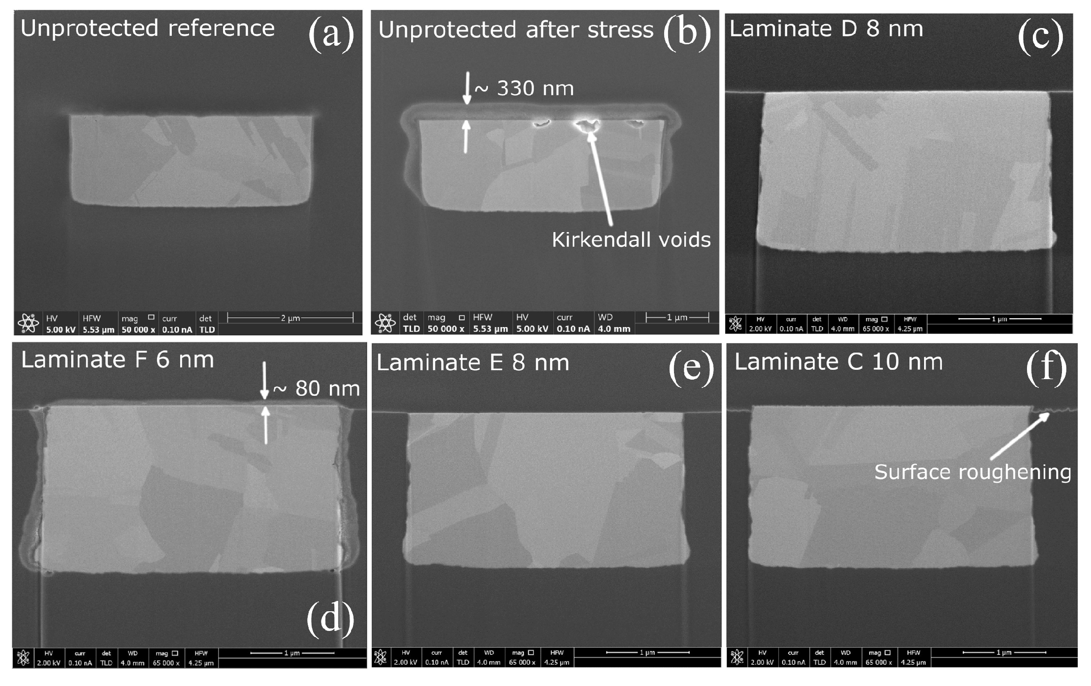
- Chery, E.; Brady-Boyd, A.; Lin, Y.; Grimes, M.; Springer, D.; Slabbekoorn, J.; Walsby, E.; Croes, K.; Beyne, E. Vapor deposited thin organic–inorganic capping layers preventing copper line oxidation in polymer-based RDL technologies. Microelectron. Eng. 2022, 266, 111896. [Google Scholar] [CrossRef]
- Chery, E.; Slabbekoorn, J.; Pinho, N.; Miller, A.; Beyne, E. Advances in Photosensitive Polymer Based Damascene RDL Processes Toward Submicrometer Pitches With More Metal Layers. In Proceedings of the 2021 IEEE 71st Electronic Components and Technology Conference (ECTC), San Diego, CA, USA, 1 June–4 July 2021. [Google Scholar]
- Zhang, Y.-B.; Gao, L.-Y.; Li, X.; Li, Z.; Ma, X.-L.; Liu, Z.-Q. Electroplating nanotwinned copper for ultrafine pitch redistribution layer RDL of advanced packaging technology. In Proceedings of the 2021 22nd International Conference on Electronic Packaging Technology (ICEPT), Xiamen, China, 14–17 September 2021. [Google Scholar]
- Kwon, J.; Ju, J.; Kim, S.; Sohn, E.; Khim, J. Electromigration Performance of Fine-Line Cu Redistribution Layer (RDL) for High Density Fan Out Packaging. In Proceedings of the 2023 IEEE 73rd Electronic Components and Technology Conference (ECTC), Orlando, FL, USA, 30 May–2 June 2023. [Google Scholar]
- Tsai, M.-Y.; Lin, T.-C.; Huang, Y.-C.; Wang, S.-B.; Lin, Y.-S.; Lin, K.-L. Effect of Microstructure on the Electromigration Performance of 2-m-Cu Redistribution Line under In-situ SEM Observation. In Proceedings of the 2024 IEEE CPMT Symposium Japan (ICSJ), Kyoto, Japan, 13–15 November 2024. [Google Scholar]
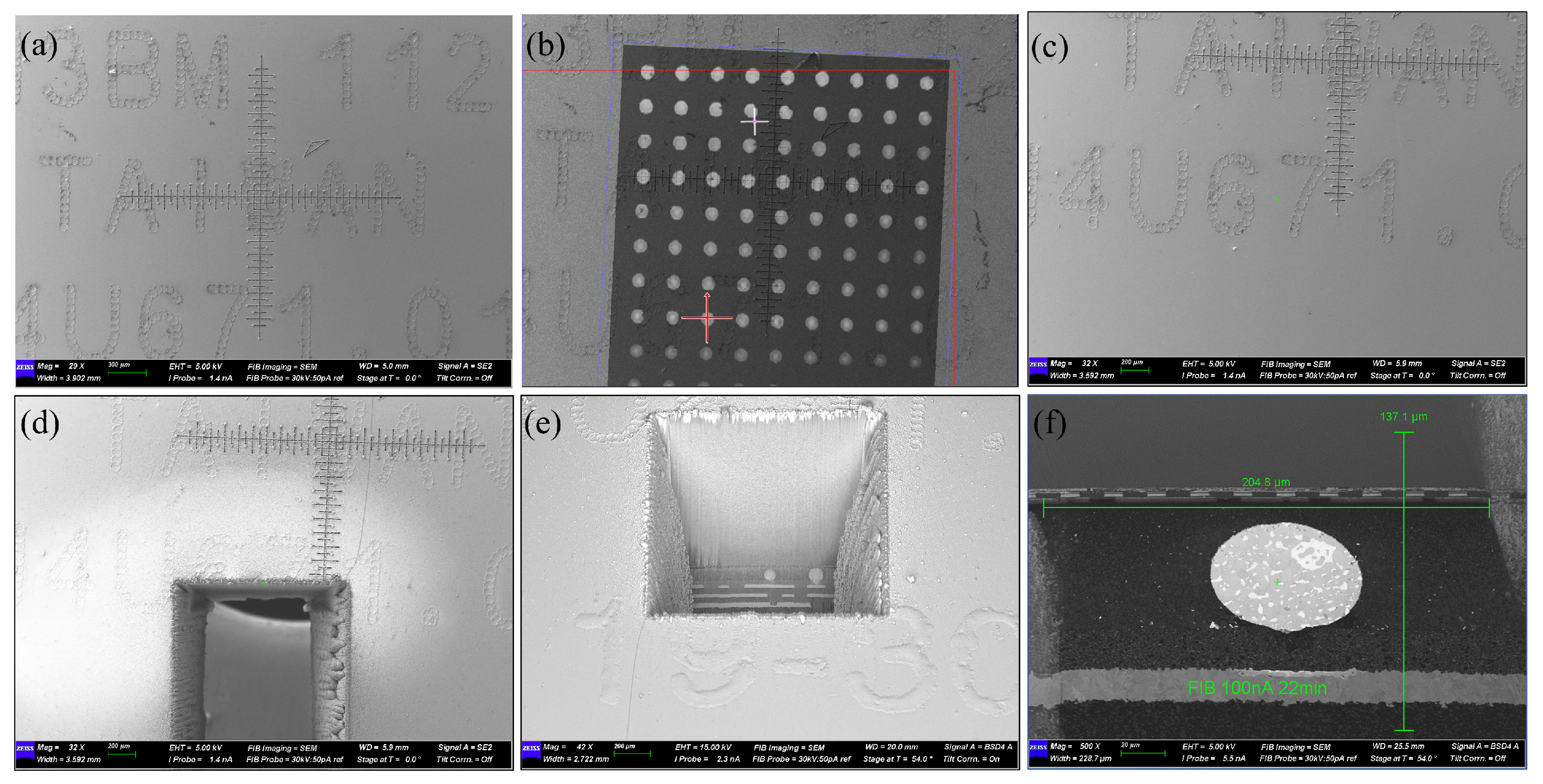
- Viswanathan, V.; Jiao, L. Developments in Advanced Packaging Failure Analysis using Correlated X-Ray Microscopy and LaserFIB. In Proceedings of the 2021 IEEE 23rd Electronics Packaging Technology Conference (EPTC), Singapore, 7–9 December 2021. [Google Scholar]
- Viswanathan, V.; Maeda, E.; Yamamoto, C.; Oda, T.; Jiao, L. Targeted Sample Preparation and Analysis of Advanced Packaging using Correlated X-Ray Microscopy and Laser FIB. In Proceedings of the 2022 IEEE CPMT Symposium Japan (ICSJ), Kyoto, Japan, 9–11 November 2022. [Google Scholar]
- Zhang, S.Y.; Zhang, Y.J.; Kwek, W.M.; Goi, L.S.; Trigg, A.D.; Tang, L.J. Application of Transmission EBSD on high topography surface Aluminum thin film. In Proceedings of the 2014 IEEE 16th Electronics Packaging Technology Conference (EPTC), Singapore, 3–5 December 2014. [Google Scholar]
- Wang, C.; Luo, K.; He, P.; Zhou, H.; Li, R.; Zhang, Z.; Yu, D.; Zhang, S. Quasi in-situ observation of Ni-plated solder from various fracture mechanism using EBSD. J. Mater. Res. Technol. 2023, 24, 1875–1881. [Google Scholar] [CrossRef]
- Wakamoto, K.; Yasugi, D.; Otsuka, T.; Nakahara, K.; Namazu, T. Fracture Mechanism of Sintered Silver Film Revealed by In Situ SEM Uniaxial Tensile Loading. IEEE Trans. Components Packag. Manuf. Technol. 2024, 14, 240–250. [Google Scholar] [CrossRef]
- Auersperg, J.; Vogel, D.; Auerswald, E.; Rzepka, S.; Michel, B. Nonlinear Copper Behavior of TSV and the Cracking Risks during BEoL-Built-up for 3D-IC-Integration. In Proceedings of the 2012 13th International Thermal, Mechanical and Multi-Physics Simulation and Experiments in Microelectronics and Microsystems, Cascais, Portugal, 16–18 April 2012. [Google Scholar]
- Belu, A.M.; Graham, D.J.; Castner, D.G. Time-of-flight secondary ion mass spectrometry: Techniques and applications for the characterization of biomaterial surfaces. Biomaterials 2003, 24, 3635–3653. [Google Scholar] [CrossRef]
- Chelgani, S.C.; Hart, B. TOF-SIMS studies of surface chemistry of minerals subjected to flotation separation—A review. Miner. Eng. 2014, 57, 1–11. [Google Scholar] [CrossRef]
- Costina, A.; Wöhrmann, M.; Schiffer, M.; Schneider-Ramelow, M. Manufacturing and Characterization of Thin-Film Tantalum Pentoxide Integrated Capacitors. In Proceedings of the 2024 IEEE 10th Electronics System-Integration Technology Conference (ESTC), Berlin, Germany, 11–13 September 2024. [Google Scholar]
- Klengel, R.; Bennemann, S.; Schischka, J.; Grosse, C.; Petzold, M. Advanced Failure Analysis Methods and Microstructural Investigations of Wire Bond Contacts for Current Microelectronic System Integration. In Proceedings of the 2009 European Microelectronics and Packaging Conference, Rimini, Italy, 15–18 June 2009. [Google Scholar]


Disclaimer/Publisher’s Note: The statements, opinions and data contained in all publications are solely those of the individual author(s) and contributor(s) and not of MDPI and/or the editor(s). MDPI and/or the editor(s) disclaim responsibility for any injury to people or property resulting from any ideas, methods, instructions or products referred to in the content. |
© 2025 by the authors. Licensee MDPI, Basel, Switzerland. This article is an open access article distributed under the terms and conditions of the Creative Commons Attribution (CC BY) license (https://creativecommons.org/licenses/by/4.0/).
Share and Cite
Zhang, H.; Ma, M.; Liu, Y.; Zhang, W.; Zhang, C. Recent Applications of Focused Ion Beam–Scanning Electron Microscopy in Advanced Packaging. J. Manuf. Mater. Process. 2025, 9, 158. https://doi.org/10.3390/jmmp9050158
Zhang H, Ma M, Liu Y, Zhang W, Zhang C. Recent Applications of Focused Ion Beam–Scanning Electron Microscopy in Advanced Packaging. Journal of Manufacturing and Materials Processing. 2025; 9(5):158. https://doi.org/10.3390/jmmp9050158
Chicago/Turabian StyleZhang, Huan, Mengmeng Ma, Yuhang Liu, Wenwu Zhang, and Chonglei Zhang. 2025. "Recent Applications of Focused Ion Beam–Scanning Electron Microscopy in Advanced Packaging" Journal of Manufacturing and Materials Processing 9, no. 5: 158. https://doi.org/10.3390/jmmp9050158
APA StyleZhang, H., Ma, M., Liu, Y., Zhang, W., & Zhang, C. (2025). Recent Applications of Focused Ion Beam–Scanning Electron Microscopy in Advanced Packaging. Journal of Manufacturing and Materials Processing, 9(5), 158. https://doi.org/10.3390/jmmp9050158