Article

Injection Compression Molding of LDS-MID for Millimeter Wave Applications

1
Institute for Micro Integration (IFM), University of Stuttgart, Allmandring 9b, 70569 Stuttgart, Germany
2
Hahn-Schickard, Allmandring 9b, 70569 Stuttgart, Germany
*
Author to whom correspondence should be addressed.
J. Manuf. Mater. Process. 2023, 7(5), 184; https://doi.org/10.3390/jmmp7050184
Submission received: 6 September 2023 / Revised: 29 September 2023 / Accepted: 4 October 2023 / Published: 13 October 2023

Abstract

:
LDS-MIDs (laser direct structured mechatronic integrated devices) are 3D (three-dimensional) circuit carriers that are used in many applications with a focus on antennas. However, thanks to the rising frequencies of HF (high-frequency) systems in 5G and radar applications up to the mmWave (millimeter wave) region, the requirements regarding the geometrical accuracy and minimal wall thicknesses for proper signal propagation in mmWave circuits became more strict. Additionally, interest in combining those with 3D microstructures like trenches or bumps for optimizing transmission lines and subsequent mounting processes is rising. The change from IM (injection molding) to ICM (injection compression molding) could offer a solution for improving the 3D geometries of LDS-MIDs. To enhance the scientific insight into this process variant, this paper reports on the manufacturing of LDS-MIDs for mmWave applications. Measurements of the warpage, homogeneity of local wall thicknesses, and replication accuracy of different trenches and bumps for mounting purposes are presented. Additionally, the effect of a change in the manufacturing process from IM to ICM regarding the dielectric properties of the used thermoplastics is reported as well as the influence of ICM on the properties of LDS metallization—in particular the metallization roughness and adhesion strength. This paper is then concluded by reporting on the HF performance of CPWs (coplanar waveguides) on LDS-MIDs in comparison to an HF-PCB.

1. Introduction

Radar and communication technology have been constantly evolving over the last few decades. To make radars more precise and transmit ever-growing amounts of data, the used frequencies are increasing constantly. Over the last two decades, especially the mmWave (millimeter wave) frequency range between 30 and 300 GHz gained more and more attention, as the MMIC (monolithic microwave integrated circuit) technology evolved and chipsets for those high frequencies integrated more functionality in a smaller form factor and at a comparably low price. In particular, the frequency range between 30 and 80 GHz is currently experiencing a phase of broad commercialization driven by the allocation of 60 and 80 GHz [1] frequency bands for radar applications as well as 20–40 GHz and 60 GHz bands for communication.
But while the increasing frequencies offer better HF (high-frequency) systems, they also increase the constraints on physical components. Reasons therefore are the converse scaling of HF components with an increase of frequencies and increasing losses in HF components due to dielectric, metallic, and radiation losses. Those losses cause higher power uptake and heat generation within the HF system and are partly linked to the manufacturing tolerances.
So, the HF community is continuously searching for novel technologies and designs to improve the performance of their HF systems and limit the amount of power uptake and excess heat generation.
While a trend in designing mmWave systems involves the integration of antennas directly into the MMIC package [2], placing antennas on an interconnection substrate is still an important way of realizing application-specific solutions. The most typical way involves HF-capable PCBs (printed circuit boards) with a high number of layers. In these HF designs, the layers are required to realize 3D geometries for antennas, separate different signal-carrying layers through power supply and ground planes, and avoid warping through symmetrical build-ups. However, the individual structuring steps and sequential laminating processes lead to rapidly increasing costs with simultaneously increasing tolerances [3]. In particular, the thickness tolerance of these layer stacks can reach up to 10%. This can have a negative impact on the HF performance of the antennas and the overall system. While this is a proven and over the years thoroughly tested technology, the PCBs’ limitation to 2D (two-dimensional) layer stacks impairs their performance at frequencies in the mmWave region, as superior EM (electromagnetic) field modification can be achieved with 3D structures. However, the modification of primarily 2D substrates can be beneficial.
Advanced transmission line structures, also known as micromachined transmission line structures, can offer especially low losses and improved performance [4,5,6,7,8,9,10,11,12,13]. While most of the publications are dedicated to structures on silicon, some publications are available that deal with such structures on PCB substrates [6,8,10]. The main drawback of micromachined structures on PCBs is the sequential mechanical milling or laser milling process that is necessary to form the structures needed.
While metal-plated plastics and in some capacity 3D-printed devices are used to complement HF-PCBs in many cases, they lack the combination of 3D structures with the metallization of sufficient conductivity, small features like line and isolation width, and the capability to manufacture VIAs (vertical interconnect accesses) on two or more layers.
A class of circuit carriers that fits into this gap includes MIDs (mechatronic integrated devices) [14], which have been used in low-frequency antenna applications for more than 20 years. Their main usage is in conformal antennas for handheld devices [14], but surface-mountable antennas are also available on the market [15], and designs exist to use them in base station applications [16,17].
MIDs combine in most cases injection-molded plastic bodies with an electrical circuit on their surface. While this approach lacks the multi-layer capability of PCBs, it offers the possibility of utilizing the 3D space. Additionally, the manufacturing tolerances of the dielectric substrate can be significantly smaller than for most PCB processes. The utilization of MID as a submount for MMIC and antennas on the digital PCBs responsible for data processing could combine the benefits of both technologies.
The most prominent technology in this regard is the LDS (laser-direct structuring)-MID technology. In this technology, a thermoplastic base material is mixed with an LDS additive, e.g., a copper–chromium spinel, which can be activated by laser structuring. In the manufacturing process, after the original shaping by plastic injection molding, the desired circuit layout and all VIAs are structured or drilled by an infrared laser. The LDS-MIDs are then prepared for electroless copper deposition by removing the laser debris in a subsequent cleaning process. Finally, the circuit is protected from environmental influences with a finish, usually Ni/Au (ENIG, electroless nickel/immersion gold), and fitted with SMDs (surface-mounted devices).
As the acceptable tolerances in the mmWave range continue to decrease, the LDS-MID technology must also be optimized in this regard. ICM (injection–compression molding) can be used to optimize the geometric deviations caused by shrinkage and distortion during primary shaping. In this process variation of IM (injection molding), the mold is not completely closed before injection. To prevent the melt from escaping, special plunge edge molds are needed. During or after the injection process, the mold is completely closed, and the compression pressure is applied. Through this, the pressure is applied homogeneously. This leads to significantly improved shrinkage and warpage. In addition, compared to injection molding, injection–compression-molded parts can be produced with significantly thinner walls and longer flow paths [18]. These thinner wall thicknesses are for example necessary to reduce the distances between signal conductors (on the top layer) and ground surfaces (on the bottom layer) in mmWave HF systems, as this wall thickness is one of the critical parameters that determine the cut-off frequency of higher-order propagation modes.
The ICM of LDS-capable thermoplastics has already been investigated in [19] for use in a hybrid sensor manufacturing process. Bengsch et al. have primarily dealt with the molding of surface structures with low aspect ratios in the sub µm or low single digit µm range, the planarity, and surface roughness of the ICM substrates.
To realize the potential of MID in mmWave applications, the usable materials need to be analyzed and optimized, process steps have to be modified to meet the demands, and design methodology and software tools need to be upgraded to better handle 3D aspects in novel applications.
This paper describes the utilization of ICM to manufacture LDS-MIDs with certain geometries beneficial for mmWave applications and the overall effect of changing the manufacturing method from IM to ICM. This is necessary because the LDS process can be particularly sensitive regarding the molding process, as optimal metallization not only depends on the material itself and the laser and metallization parameters: the surface morphology is as important. For example, can high roughness cause spurious metallization on unstructured areas of the LDS-MIDs? Additionally, the surface of a molded part can be locally impoverished with LDS fillers due to unwanted effects during injection molding, which can cause faulty metallization.
In contrast to [19], we discuss the impact of injection–compression molding on the molding accuracy of more complex geometries with higher wall thickness differences and different materials. Moreover, the effects on the dielectric properties of LDS-MID plastics and the LDS-MID metallization are presented. The paper is then concluded by presenting insertion loss measurements of CPW lines on LDS-MIDs. All of those aspects have not yet been dealt with in the literature.

2. Materials and Methods

2.1. Materials

Three LDS-MID thermoplastics were selected for the presented investigations. Firstly, a commodity plastic of the Xantar 3760 LDS (Mitsubishi Engineering Plastics Corporation, Tokio, Japan, hereinafter PC LDS) [20] type, a modified PC (polycarbonate), was chosen. From the range of high-temperature thermoplastics, the LCP (Liquid Crystal Polymer) Tecacomp LCP LDS black 4107 (Ensinger GmbH, Nufringen, Germany, hereinafter LCP LDS) [21] and the PEEK (polyetheretherketone) Tecacomp PEEK LDS black 1047045 (Ensinger GmbH, Nufringen, Germany, hereinafter PEEK LDS) [22] were selected. PC LDS was chosen, as it is the main material for antenna applications at lower frequencies (up to 6 GHz) in 3G and 4G applications. LCP LDS, on the other hand, is filled with a high amount of talc fillers and dominates the market in the field of lead-free solderable LDS-MIDs. The PEEK LDS was chosen because it promises better dielectric properties, better adhesion of the metallization, and superior isotropy compared to LCP LDS. Additionally, it contains the same filler technology as LCP LDS, which enables better comparability. The substrates examined include injection-molded plates with dimensions of 37 × 37 × 1.5 mm 3 and injection–compression-molded round plates with a diameter of 60 mm. The HF circuit board materials Ro4350b (Rogers Corporation, Chandler, AZ, USA) [23] and TSM-DS3 (Taconic ltd, Petersburgh, NY, USA) [24] are used as HF-related reference materials. The substrates made of these HF-PCB materials were purchased externally.

2.2. Analytical Methods

The VR-6200 profilometer (Keyence Corporation, Osaka, Japan) was used to analyze the geometry of the entirety of the samples. This device uses the principle of structured light projection. A CLSM (confocal laser scanning microscope) VK-X 1000/3000 (Keyence Corporation, Osaka, Japan) was used for surface analysis of roughness and local optical analysis.
The adhesive strength of the metallization was determined utilizing an HBP (hot-bump-pull) test on a Nordson Dage 4000Plus bond testing unit (Nordson Corporation, Westlake, OH, USA). The test procedure starts with soldering a copper pin onto a round pad with a diameter of 0.9 mm. Detailed soldering profiles are reported in [25]. After a cooling period, it is then pulled off vertically, and the force maximum is logged.
To be able to determine changes in the dielectric material properties due to the change from IM to ICM, the method of parallel plate capacitor measurement was used. A thin sample of the dielectric material to be examined is clamped between two electrodes of a capacitor. This setup is then measured with an impedance analyzer. The 16453A Test Fixture and Keysight E4991A Impedance/Materials Analyzer (Keysight Technologies, Santa Rosa, CA, USA) were used for the measurements presented here. This method allows for the characterization of the relative permittivity Dk and the dissipation factor Df up to a value of 1 GHz.

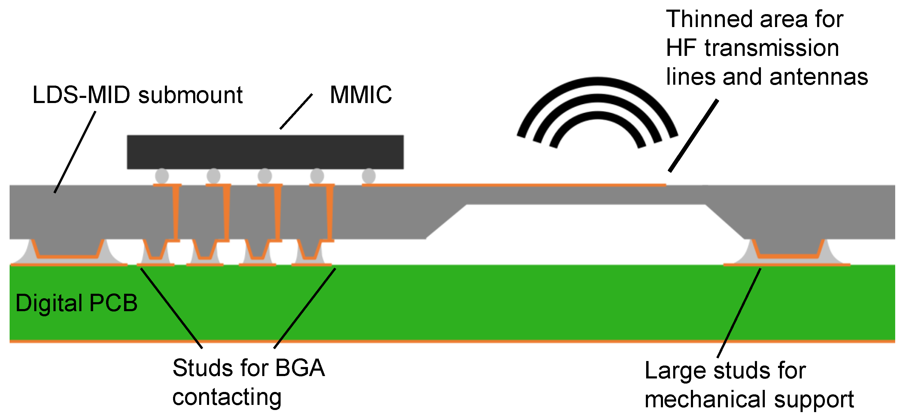
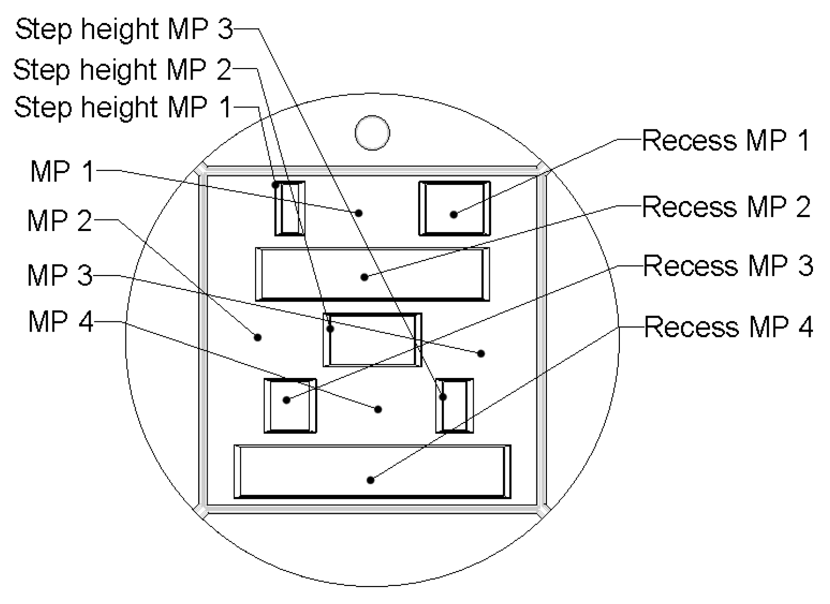
2.3. Component Design
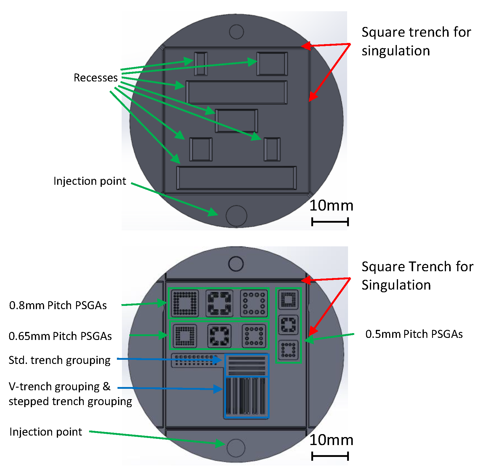
As shown in Figure 1, the basic design concept idea for future mmWave LDS-MIDs submounts combines a printed circuit board for digital signal processing and an LDS-MID for the analog RF circuitry. The signal-generating MMIC is soldered onto the LDS-MID. The majority of its contacts are connected to the PCB via an array of metalized polymer studs, which is called a polymer stud grid array (PSGA). Outside this PSGA, the LDS-MID is electrically contacted and mechanically fixed to the PCB via additional larger polymer studs. To transport the high-frequency signals ideally on the LDS-MID, wall thicknesses are reduced locally. These thinned areas can also provide optimization possibilities for microstrip patch antennas.
To analyze the ICM manufacturing process regarding the necessary geometry, two parts were designed. As the main focus of this paper is to limit the cost of the used manufacturing processes, a circular outline for the parts is used. The reasoning behind this choice is an easier implementation of the plunging edge in a circular part as in an arbitrary form, as standard lathing methods can be used instead of electrical discharge machining. Furthermore, geometries were milled in hardened steel only and not into a nickel stamper, and no anti-stick coating was applied to shorten the manufacturing cycle of the mold.

Disc 1

The design for disc 1 consists of a flat plate with large recesses; see Figure 2 on the left side. These are intended to reduce the wall thickness locally for high-frequency transmission lines. The different lengths of the recesses correspond to the individual components of a calibration layout for such high-frequency transmission lines. This should be used to examine the HF performance of the injection–compression-molded LDS-MID. It follows the TRL (through, reflect, line) standard. This calibration is used to extract the measurement influences of the network analyzer, the feed lines, and measuring tips from the measurement response. A so-called CPW (coplanar waveguide) transmission line is selected as the line type for the TRL kit. The designed layout can be seen in Figure 3. The overall target for the wall thickness of the part is 700 µm with a targeted wall thickness in the recesses of about 200 µm.
Disc 2, as seen in Figure 2 on the right side, includes an area with various high aspect ratio tapered trenches. The intended purpose of those trenches is on the one hand to pre-form VIAs to significantly reduce the laser structuring time during LDS processing. The laser processing time is one of the limiting factors in LDS-MID technology, and a large number of VIAs is often necessary in HF applications. They are used, for example, to separate transmission lines from each other by VIA fences. In addition, trenches can also be used to optimize HF transmission lines. For example, there are concepts for CPW lines to reduce the relative permittivity Dk by implementing such trenches between ground planes and the transmission line [6]. In addition, the capacitance of CPW lines on MID could be improved by metalizing the flanks of such trenches, thus miniaturizing them [26].
PSGAs were first introduced by [27,28,29,30,31] and could be used to contact LDS-MIDs on printed circuit boards. This concept has already been investigated in [32] but with larger pitches. The PSGAs in this work are adapted to typical BGA (ball grid array) pitches. Pitches of 0.8 mm, 0.65 mm, and 0.5 mm were used. In addition, arrays with double pitches (1.6 mm, 1.3 mm, and 1.0 mm) and arrays with elongated studs were included. The arrays with BGA pitches could be used to rewire an MMIC with BGA to a PCB without changing the BGA pitch. The larger arrays, on the other hand, could support and contact the LDS-MID submount outside the PSGA area. The dimensions of all PSGA arrays are shown in Table 1. Both disc designs contain a molded square trench of 40 mm 2 for singulation.

2.4. ICM

The ICM of the substrates was carried out on an ALLROUNDER 270A injection molding machine (ARBURG GmbH & Co. KG, Lossburg, Germany) with a micro-injection module. The injection–compression mold used allows quick switching of the cavity halves. To ensure processing of the PEEK material, the temperature control was also adapted, and a hot runner nozzle was installed.
The ICM process differs from the IM process, whereas an embossing step takes place after or during the melt injection. For this purpose, a frame plate with a plunge edge seals the mold while a movable stamper is in a retracted position. At a certain point during the injection process, this plunger is then moved forward, and the melt is stamped. Among other things, this significantly extends the possible flow path length, creates a homogeneous compression pressure distribution over the entire projected component surface, and compensates for inhomogeneous shrinkage [33]. The main ICM parameters are depicted in Table 2.

2.5. LDS Process

The LDS process is one of the most commonly used processes to produce three-dimensional circuit carriers. During compounding, small quantities of an LDS additive (e.g., a copper–chromium spinel) is mixed into a thermoplastic matrix material along with other fillers for mechanical and thermal property optimization.
After the 3D substrate is manufactured, mostly using injection molding, the circuit patterns are then transferred to the surface of the LDS-MID by an infrared laser. The laser roughens the surface of the plastic part, exposing and activating the LDS additive. After the LDS process, a cleaning process is needed to remove the laser debris. This is usually a wet chemical process. However, this can be supplemented, for example, by CO2 snow jet cleaning, which additionally planarizes the surface of the structured area of some LDS materials. The LDS-MIDs are then metalized in an electroless copper bath with about 10 µm copper. Subsequently, a surface finish—typically Ni/Au—is applied, but also other finishes like Pd/Au and Ag can be chosen.

3. Results

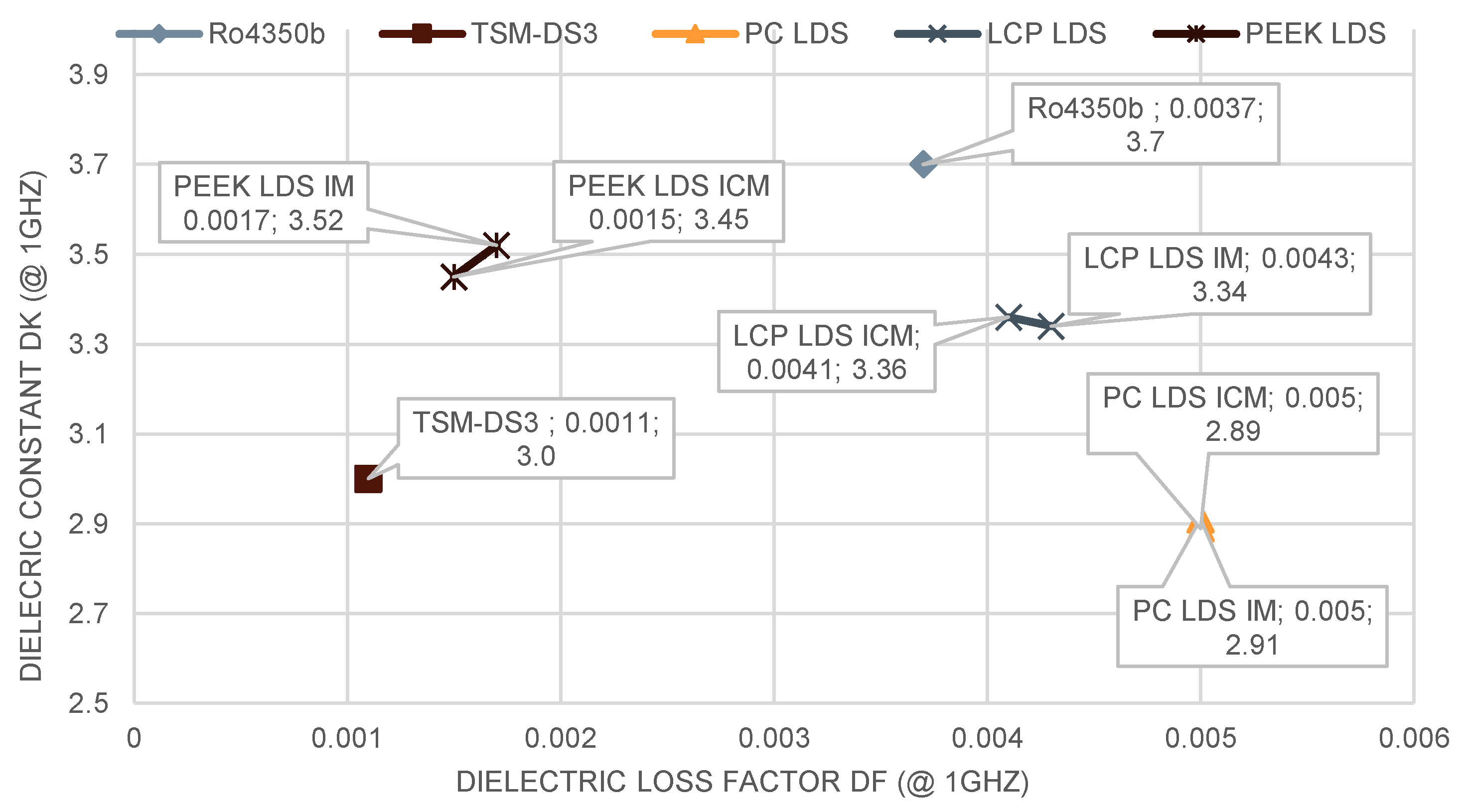
3.1. Dielectric Characterization

The results of dielectric measurements performed on IM and ICM substrates of PC LDS, LCP LDS, and PEEK LDS using the 16453A Test Fixture and Keysight E4991A Impedance/Materials Analyzer are depicted in Figure 4. It shows the dielectric properties for the 1 GHz frequency point. In addition, datasheet values of the two RF PCB materials Ro4350b and TSM-DS3 are also plotted for reference. The amorphous PC LDS shows little change in dielectric constant (DK) or dissipation factor (Df). PEEK LDS and LCP LDS show a slightly larger variation. However, these variations are still within the range of the measurement inaccuracies of the measurement system [34].

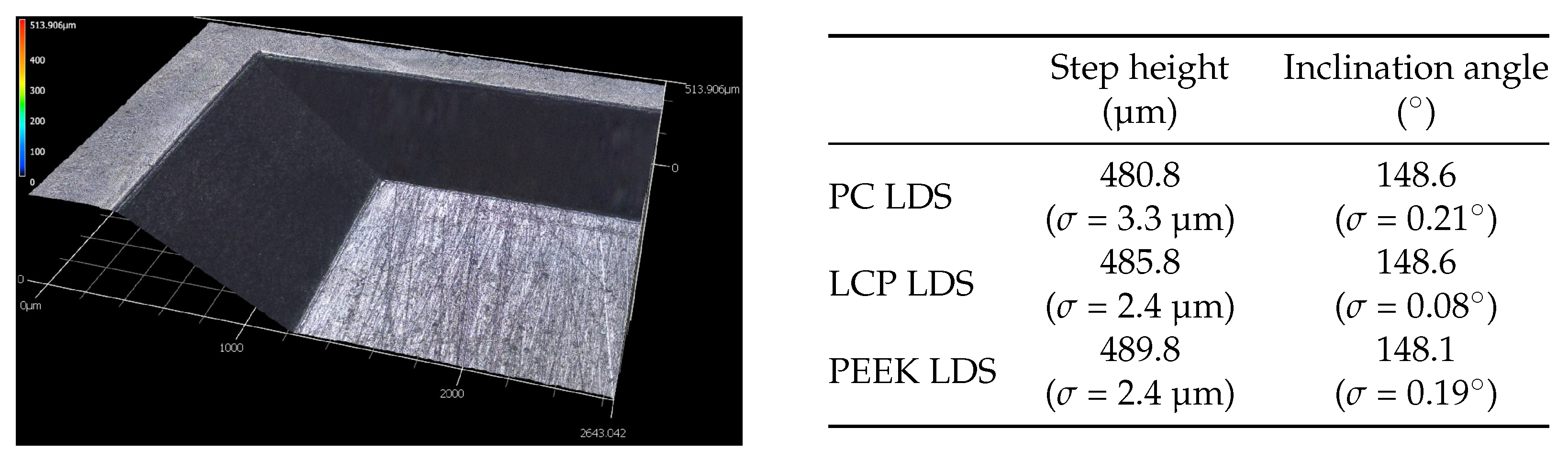
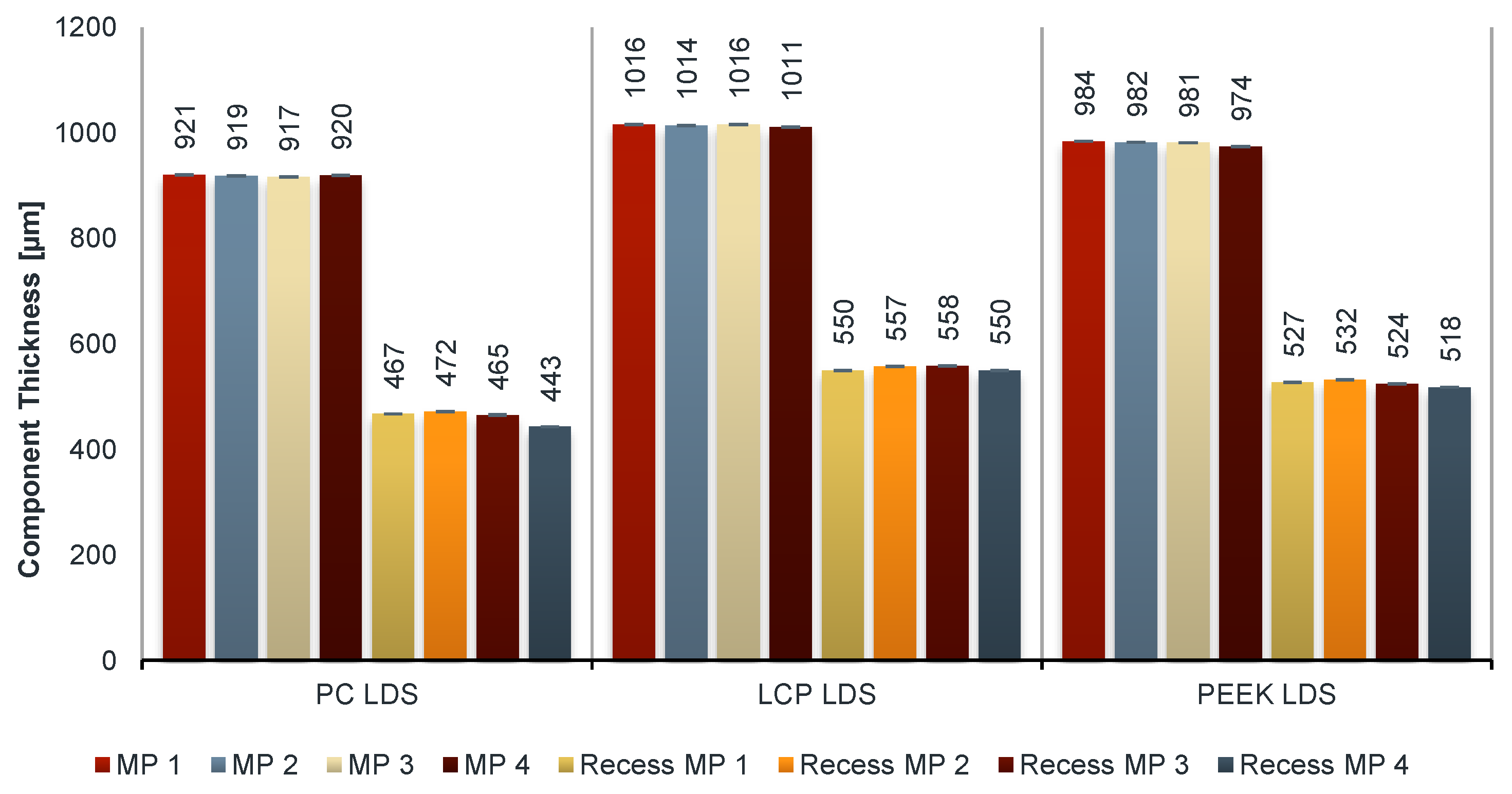
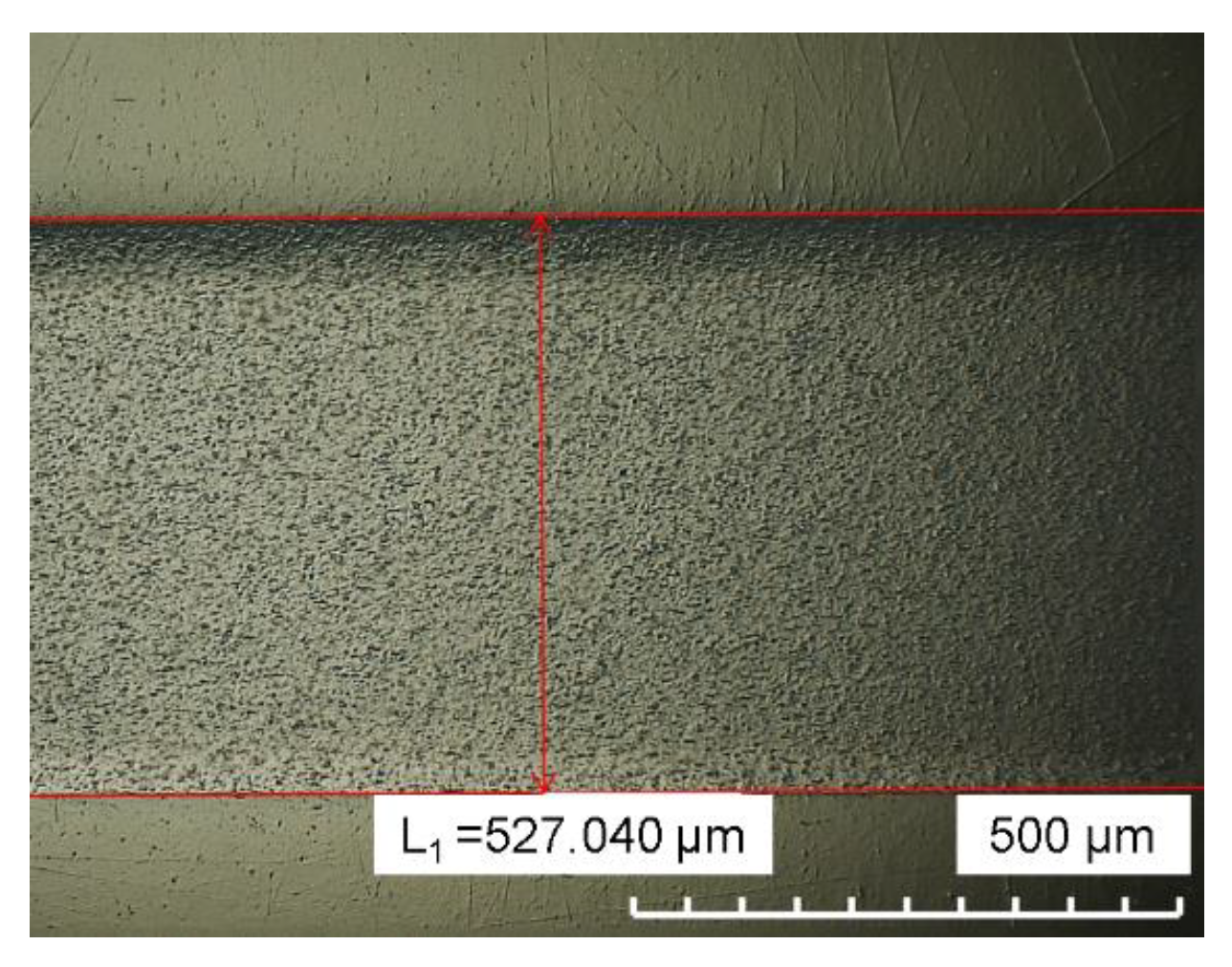
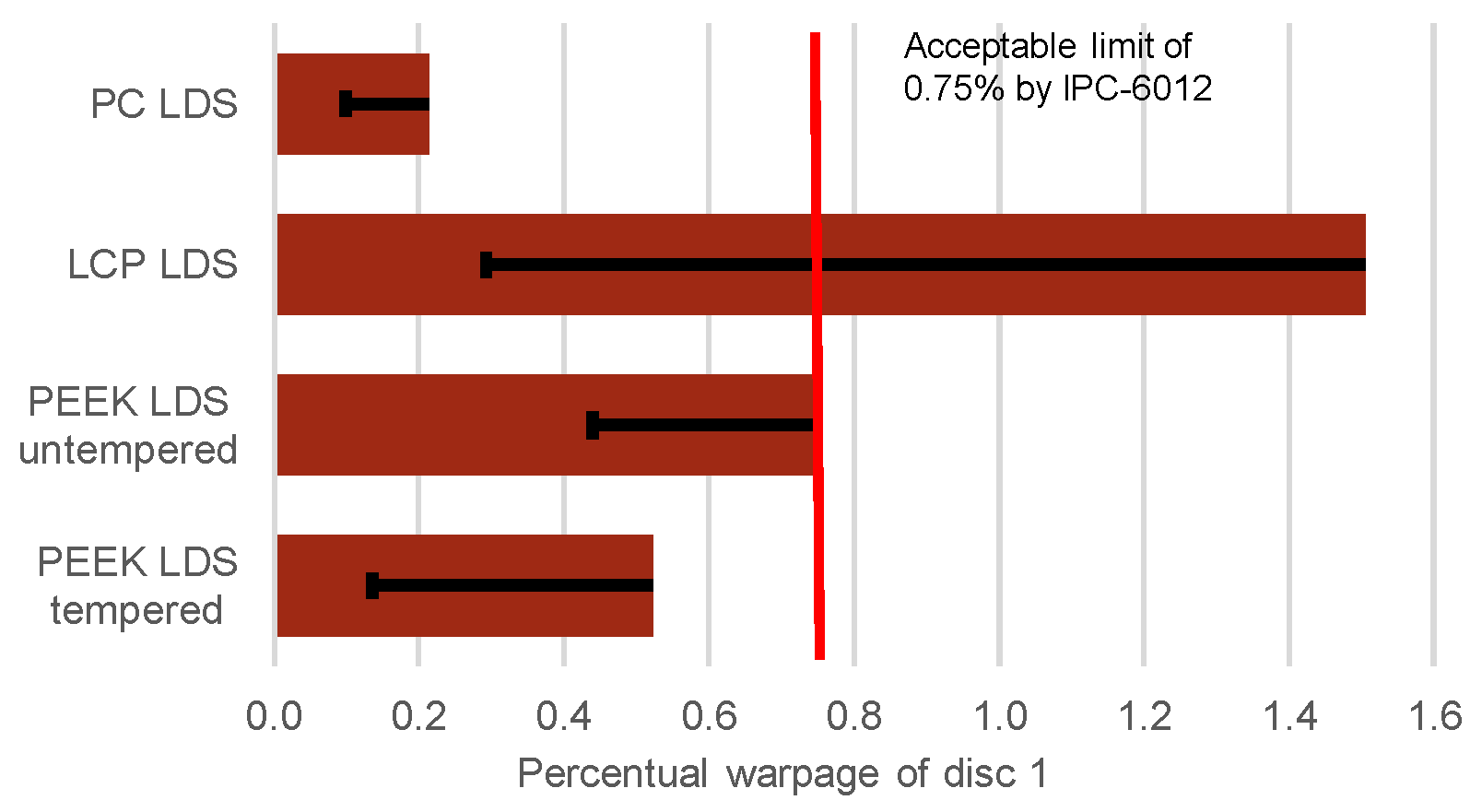
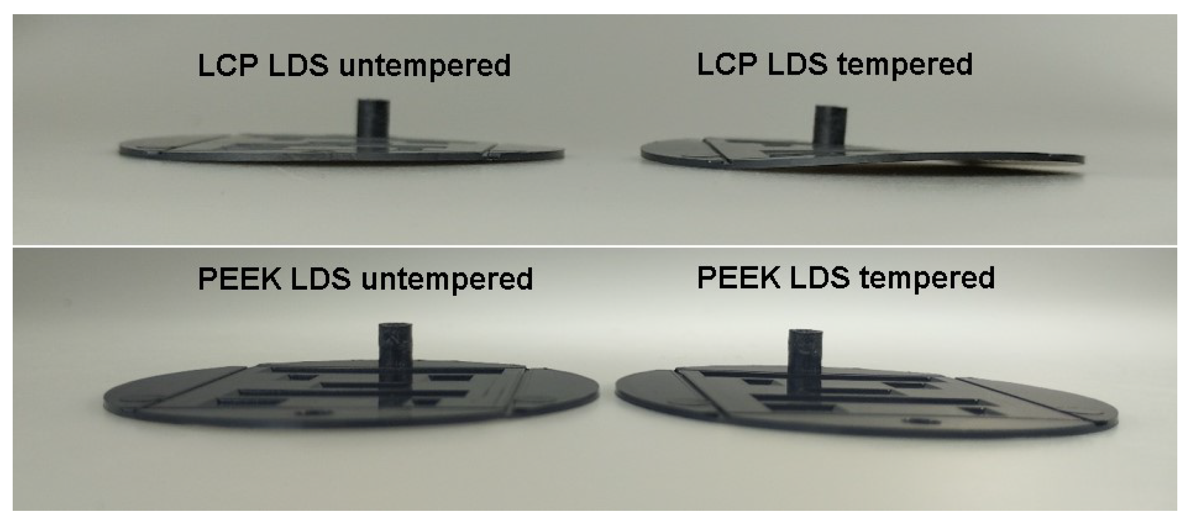
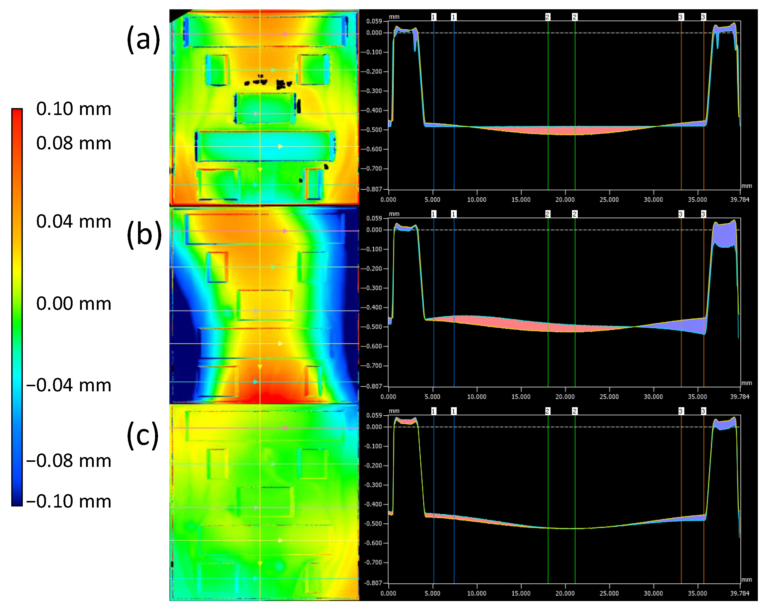
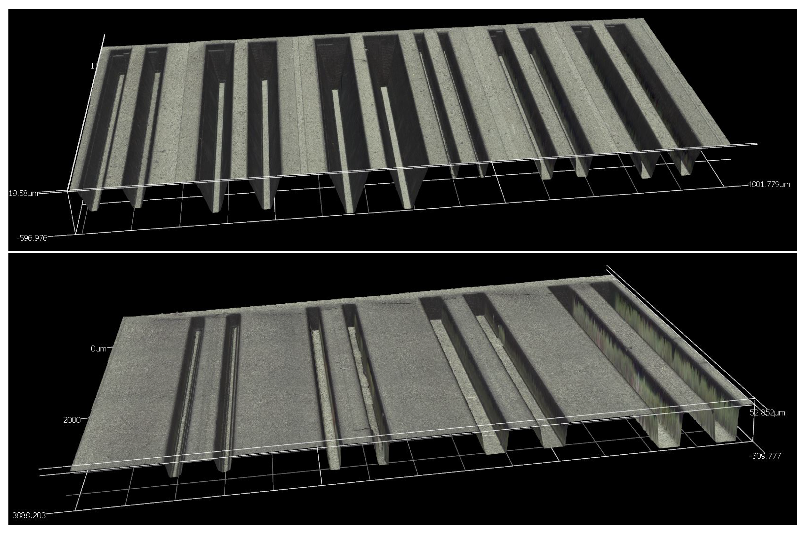
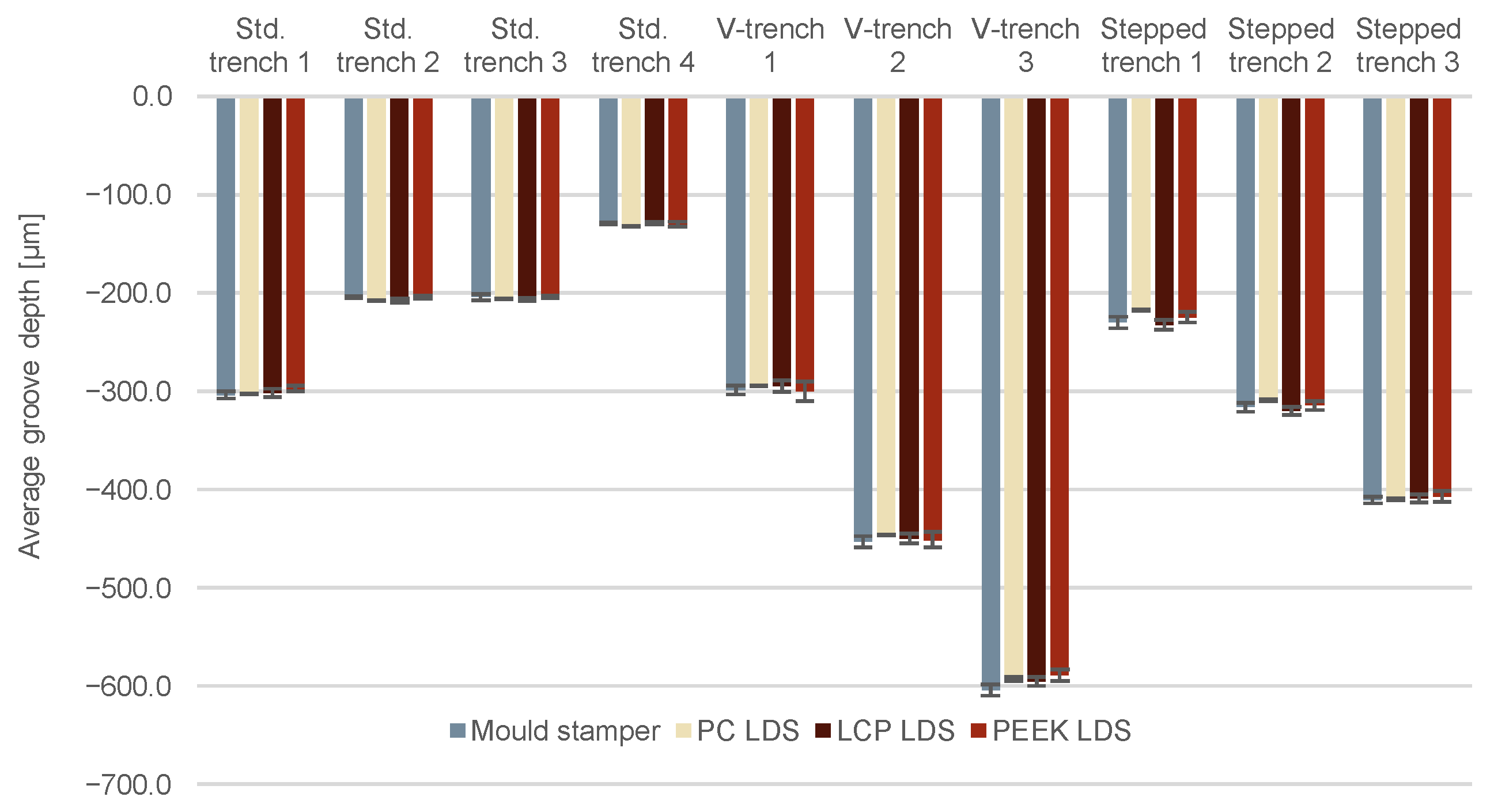
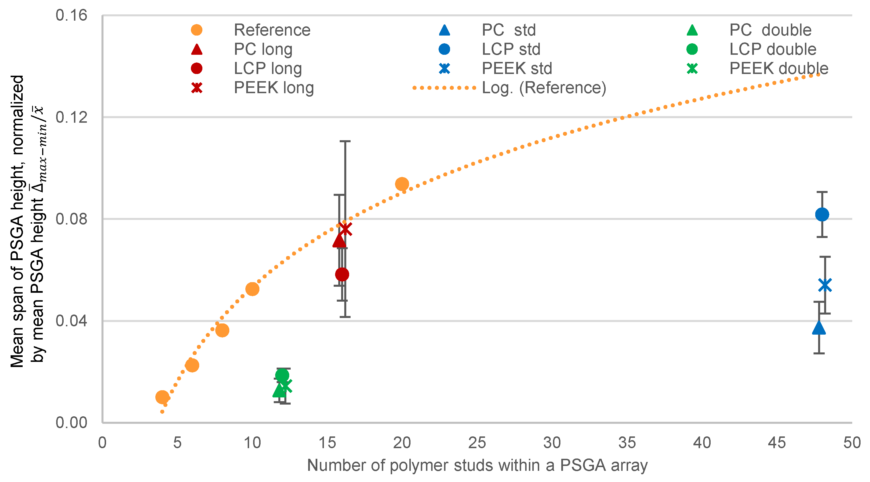
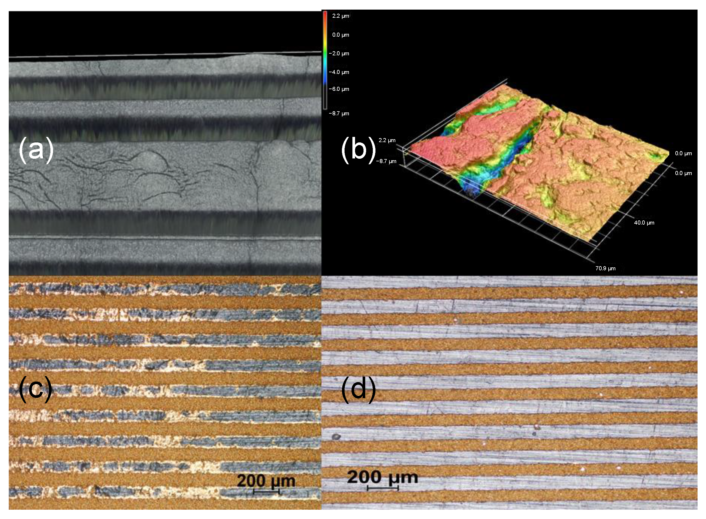
3.2. Geometrical Analysis Disc 1

The local replication accuracy of the ICM substrates was measured by means of CLSM at three positions on two parts of each type of LDS-MID substrate material. The step height of the recesses and the angle of the bevels in relation to the surface of the parts were measured.
The replication accuracy for all three LDS-MID materials investigated is shown in Figure 5. The mean values are 480.8 µm ( σ = 3.3 µm) for PC LDS substrates and 485.8 µm ( σ = 2.4 µm) and 489.8 µm ( σ = 2.4 µm) for LCP LDS substrates and PEEK LDS substrates, respectively. The differences in the mean values are presumably caused by the different melt and mold temperatures and the different coefficients of thermal expansion of the LDS-MID substrates. The angles of the ramps agree with each other with deviations of less than 1 . These results prove high replication accuracy (Figure 5).
The wall thickness was measured at four measuring points (MP) in the thick part of the plate and at four measuring points in the recesses (recess MP 1) on a total of five substrates per LDS-MID material. The measurement positions and the results are shown in Figure 6 and Figure 7. PC LDS shows the smallest wall thickness of about 915 µm, which is followed by PEEK LDS and LCP LDS with 980 µm and 1015 µm, respectively. The wall thickness in one of the larger cavities was checked on PEEK LDS by microscopic measurement of a cross-section (Figure 8). The value of approx. 527 µm measured with an optical microscope agrees with the values measured mechanically of approx. 520–530 µm in the recesses.
While the local replication accuracy of the recess and the homogeneity of the wall thicknesses of the substrates have only low single-digit tolerances, difficulties in ejecting the substrates from the injection mold were apparent during molding of the substrates. Since the mold inserts were not equipped with an anti-stick coating and only included three ejector pins, the parts jammed in the mold and were deformed during ejection, which caused warpage of the parts. This warpage was lowest for PC LDS, which was followed by PEEK LDS. Both materials met the IPC-61012 standard maximum warpage of 0.75% with respect to their edge length of 40 mm after singulation. However, LCP LDS showed a significantly larger warpage of up to 1.5% (Figure 9). To improve the planarity of the substrates, five LCP LDS and PEEK LDS substrates each were subjected to a tempering process in a box oven (2 h at 200 C). While the warpage for PEEK LDS improved significantly (Figure 9), the tempering process for LCP LDS led to an increase in warpage, see Figure 10, and was therefore discarded. Figure 11 shows the effects of the tempering step on PEEK LDS with regard to warpage. Figure 11a shows the deviation of a tempered PEEK LDS substrate from the mold insert. The more prominent sag of the recess in the upper region, near the injection point of disc 1, can be seen. In Figure 11b, the typical deviation from a tempered PEEK LDS substrate to an untempered substrate is illustrated, while Figure 11c shows the deviation between two tempered PEEK LDS substrates, which is significantly lower.
Since the recesses are of particular interest for HF signal routing, the deviations from the ideal form were also measured by means of strip light projection. As shown in Figure 12, the deviations are related to the warpage of the substrate and to the surface to wall thickness ratio of the recesses. Again, PC LDS shows the lowest warpage, which is followed by PEEK LDS tempered and untempered. LCP LDS shows the highest warpage especially in area 1. This is caused by the combination of the strain during the ejection of the disc and the special morphology of the liquid crystal polymer, which resulted in a bending of the disc.

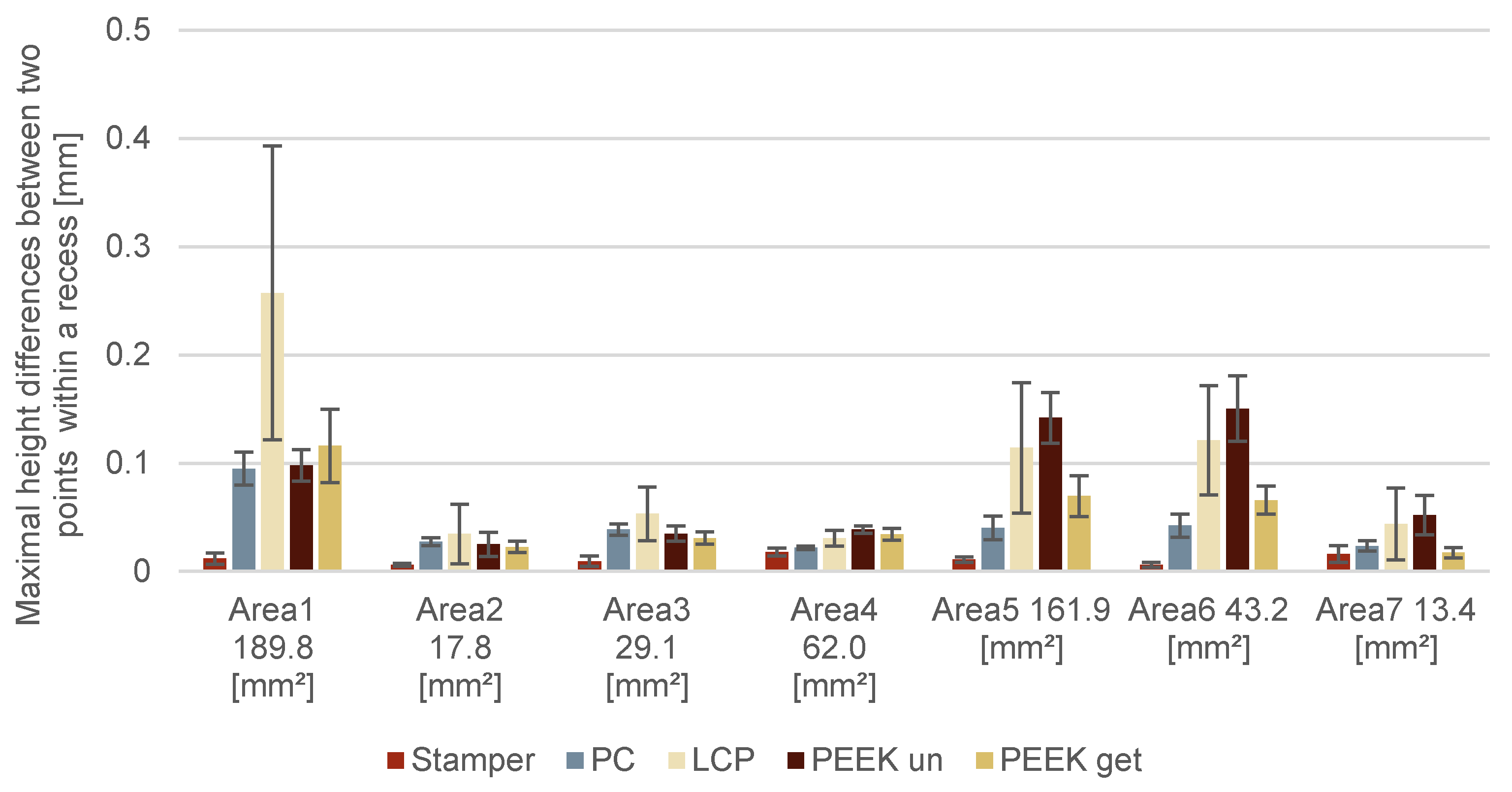
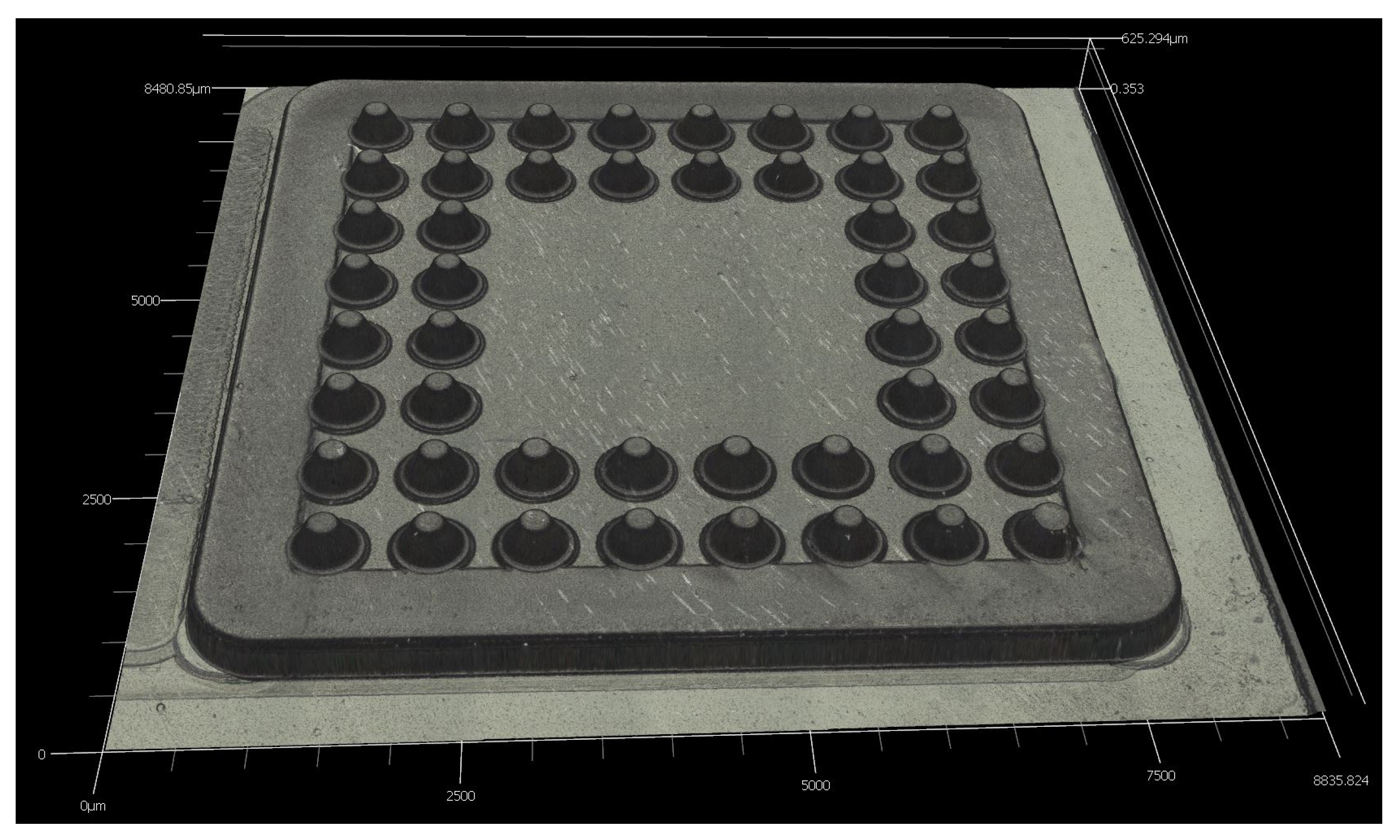
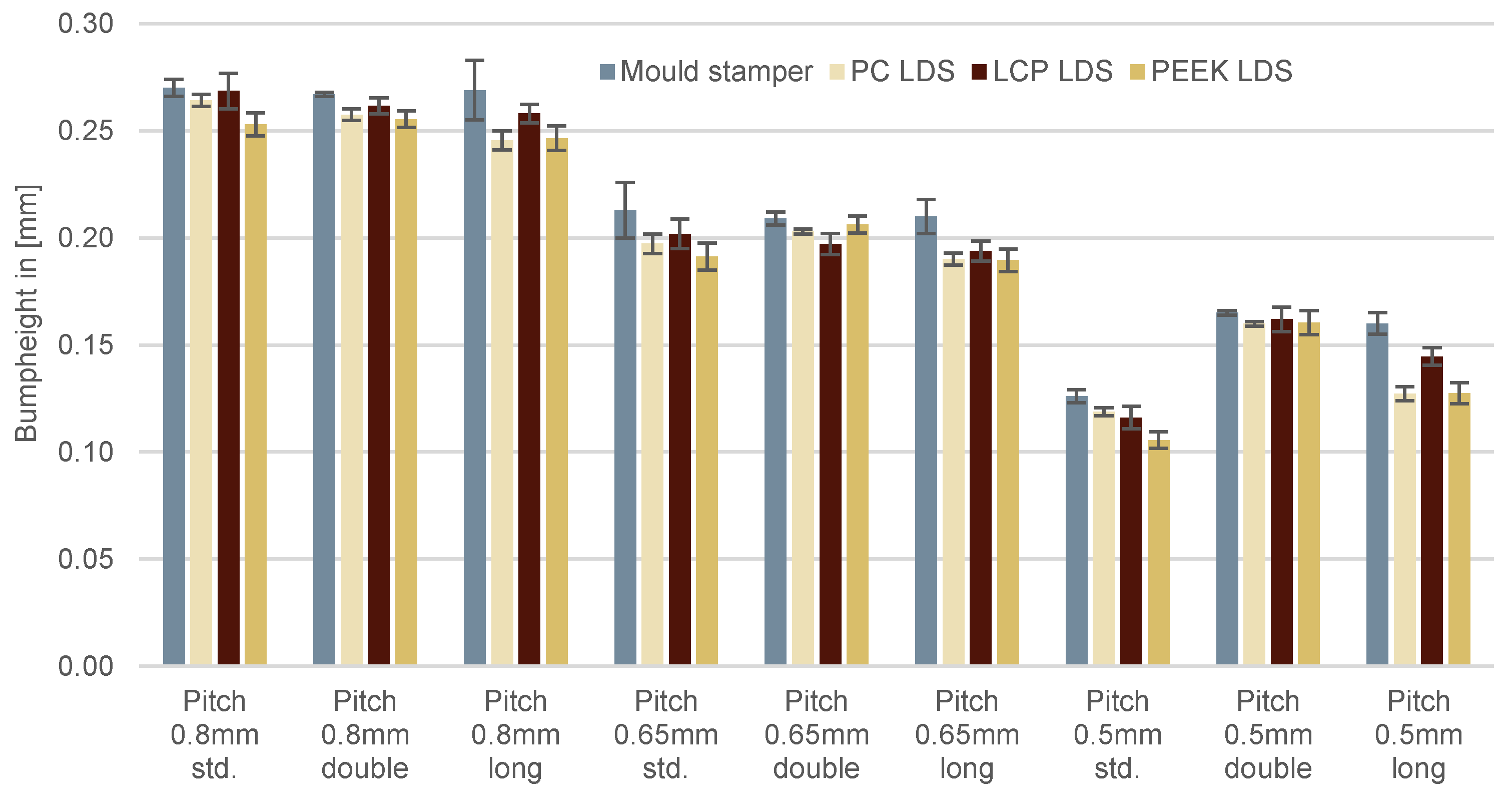
3.3. Geometrical Analysis of Disc 2

The depths of the molded trenches were measured on 10 substrates per LDS-MID material. A 3D profilometer was used. The trenches are divided into three groups. The first is a group of four by two trenches with almost perpendicular sides. They are only tapered by an angle of about five degrees to improve demolding. The second group consists of three by two V-shaped trenches with an angle of about 65 for the inclinations. The third group consists of a combination of the shapes from groups one and two. In the upper part, these trenches have a slope of 65 , while the lower halves of the trenches have an angle of 5 , as do the trenches from group one (Figure 13).
The measured trench depths showed replication rates of the trench structures are mostly between 98% and 101%. Only the replication rate for the stepped trench 1 group was at a value of only 95%. The replication rates above 100% occur not due to physical reasons but for the measurement inaccuracies of the used VR6000 strip light microscope of about ±2.5 µm (Figure 14).
Figure 15 shows a representative picture of the replicated PSGA arrays, while Figure 16 depicts the results on the overall mean stud height of all measured PSGA arrays and the overall standard deviations. Measurements were taken with the strip light method. For each material, eight stud arrays of every type were measured. In addition to the measured stud heights, the corresponding depths of the injection mold stamper are depicted. The replication rate of the standard PSGAs in the 0.8 mm pitch grouping and the 0.65 µm pitch grouping are between 90% and 99% with a mean replication rate of 94%. The 0.5 mm pitch grouping offered the lowest replication accuracy with values between 79% and 98% with a mean replication of 90%.
To determine the overall uniformity of a PSGA, the distribution of the stud heights has to be analyzed in reference to their base plane and to the leveling plane, which coincide with their settling plane. For this purpose, the mean stud height within a given array, the standard deviation, and the range of the given array were analyzed. The overall mean standard deviation within each array was 4 µm with the highest standard deviation of 8 µm, which is a mean of 2% and at the maximum only 3% of the mean height. However, when the mean spans Δ ¯ m a x m i n within the arrays are analyzed, the overall deviation is higher. Table 3 shows the mean height span within an array with the standard deviation σ Δ ¯ m a x m i n for the analyzed PSGA. To better analyze those values, in Figure 17, the mean span of the PSGA height, normalized with the mean PSGA height, is depicted alongside data from [32] which utilized IM molding of 80 µm high bumps for flip chip applications. In Figure 17, normalized by their height, all measured mean spans are below the data Kessler et al. reported. It is significant to mention that the difference in standard deviations for all arrays with elongated studs was greater in comparison to the standard deviation for all PSGAs with circular stud geometries.

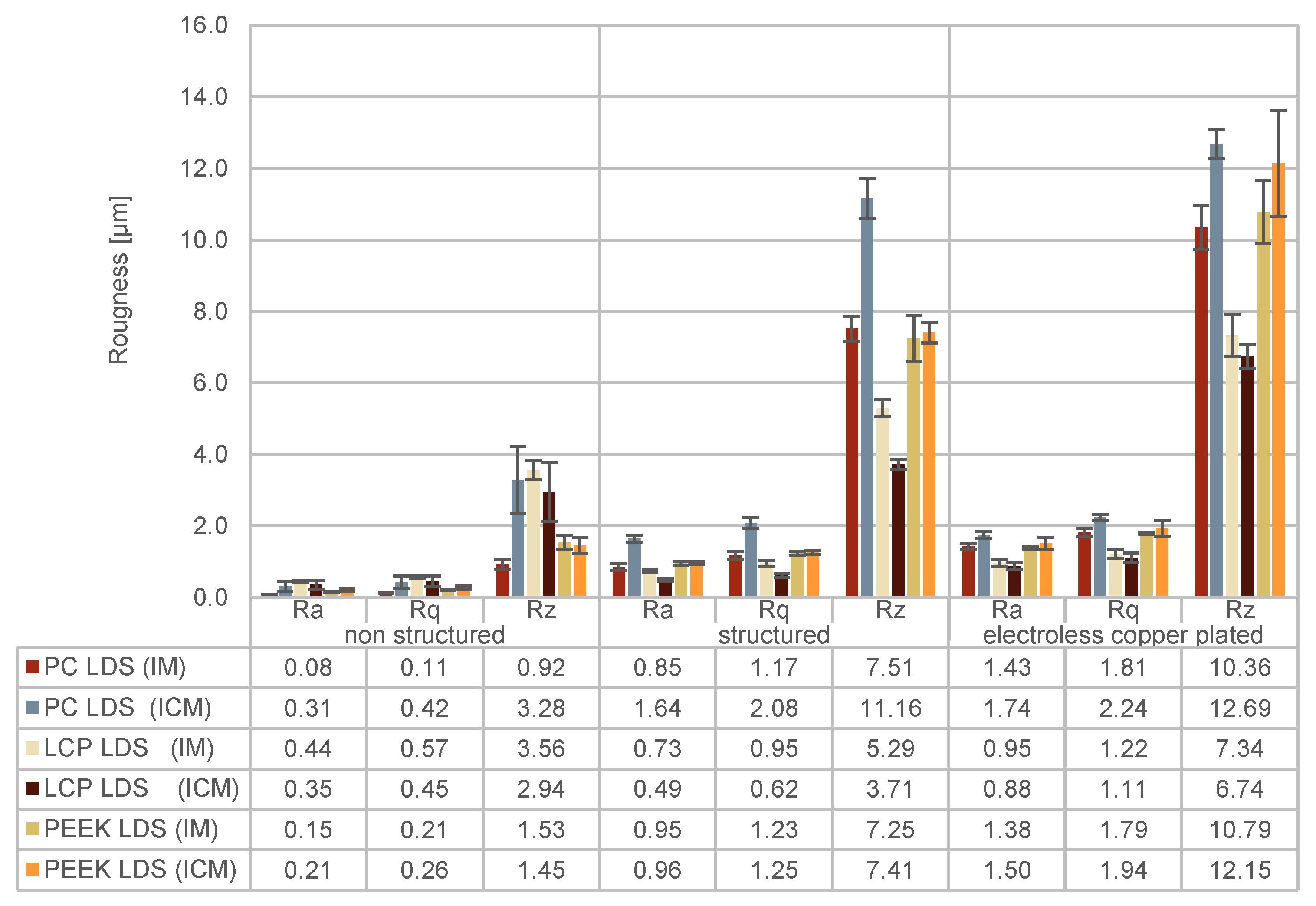
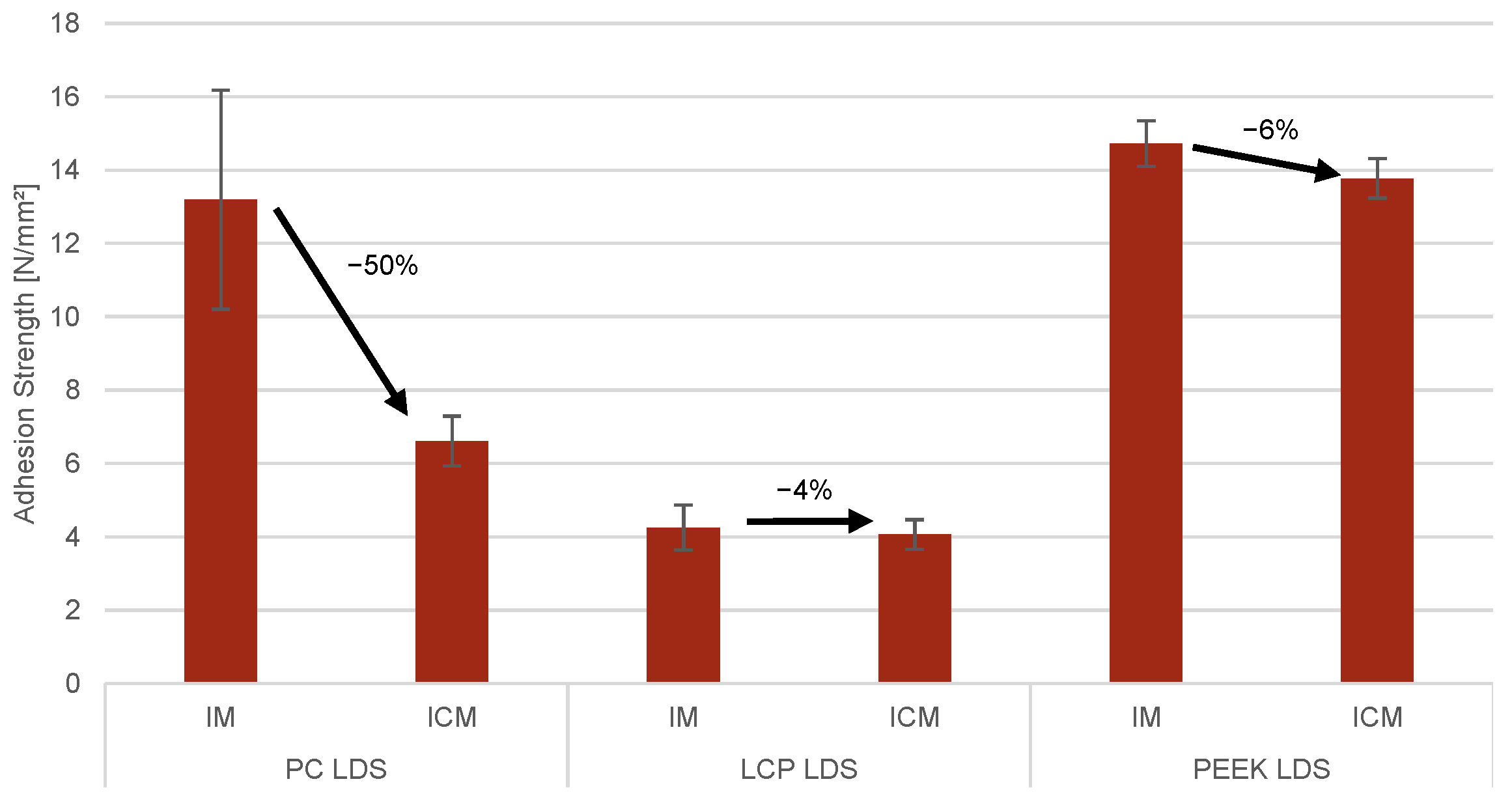
3.4. Effects of ICM on the Metallization of LDS-MIDs

To determine the effect of changing the molding process from IM to ICM on the LDS-MIDs metallization, different substrates were processed and analyzed.
While all ICM LDS-MIDs behaved similar to their IM LDS-MID counterparts regarding the initiation of metal deposition and resulting roughness, on LCP LDS, overplating can be observed, which is probably due to localized damages in its surface caused by the compression step (Figure 18).
Optical roughness measurements as well as adhesion measurements using the HBP test were carried out. The roughness on the substrates was measured on unstructured areas, laser structured and CO2 snow jet cleaned areas, and copper metallized areas. Figure 19 illustrates the results of the measurements.
To discuss the roughness, the unstructured ares have to be considered first. The roughness of an injection-molded or injection–compression-molded part is not only dependent on the mold geometry and roughness but also on the material, the design of the runner system, the mold temperatures, and the injection molding parameters. Therefore, it is reasonable that a massive change from one molding tool to another and a significant change in the injection molding process can influence the overall structure and morphology of a molded plastic part. For PC LDS, the roughness changes from Rq = 0.11 µm to Rq = 0.42 µm, and for PEEK LDS, it changes from Rq = 0.21 µm to Rq = 0.26 µm. For LCP, on the other hand, the roughness decreases from Rq = 0.57 µm to Rq = 0.45 µm. The roughness of the structured areas is not only dependent on the laser and the material. Additionally, it depends on the roughness of the molded plastic part itself, as the laser-induced roughness is only added to the existing roughness. However, this relation is not exactly linear and depends on the material properties of the plastic in interaction with the laser parameters. As each material has its own laser parameters, the comparability between materials is limited. Corresponding with the changes of the unstructured areas, the roughness of PC LDS changes from Rq = 1.17 µm to Rq = 2.08 µm, and for PEEK LDS, it changes from Rq = 1.23 µm to Rq = 1.25 µm. The roughness of structured areas on LCP LDS decreases from Rq = 0.95 µm to Rq = 0.62 µm. For the electroless copper plated areas, the roughness changed similarly from Rq = 1.81 µm to Rq = 1.24 µm for PC LDS, and for PEEK LDS, it changed from Rq = 1.79 µm to Rq = 1.94 µm. For LCP, the roughness changed the least from Rq = 1.22 µm to Rq = 1.11 µm.
The results for the adhesion measurements are shown in Figure 20. LCP LDS showed the lowest adhesion within the measurements with 4.3 N/mm 2 and 4.1 N/mm 2 for the process variations, respectively. PEEK LDS exhibited the highest adhesion strengths of 14.7 and 13.8 N/mm 2 , respectively. The variations between the adhesion measurements are only 4% and 6%. Such deviations are not uncommon due to the multitude of different influencing parameters.
PC LDS showed adhesion strengths in the range of those of PEEK LDS for substrates from the IM process. However, the adhesion strength drops when changing from IM to ICM. This may be explained by different substrate thicknesses. While the IM substrates have a thickness of about 1.5 mm, the ICM substrates used have a thickness of only 800 µm. During the pull-off of the soldered pin, the thinner substrate bends under the tensile load until the pin breaks off. This may have distorted the adhesion measurements.

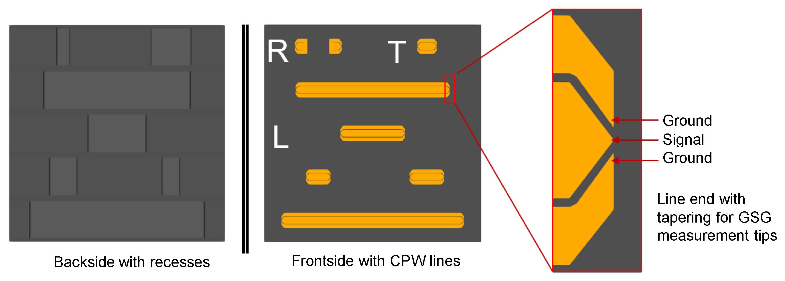
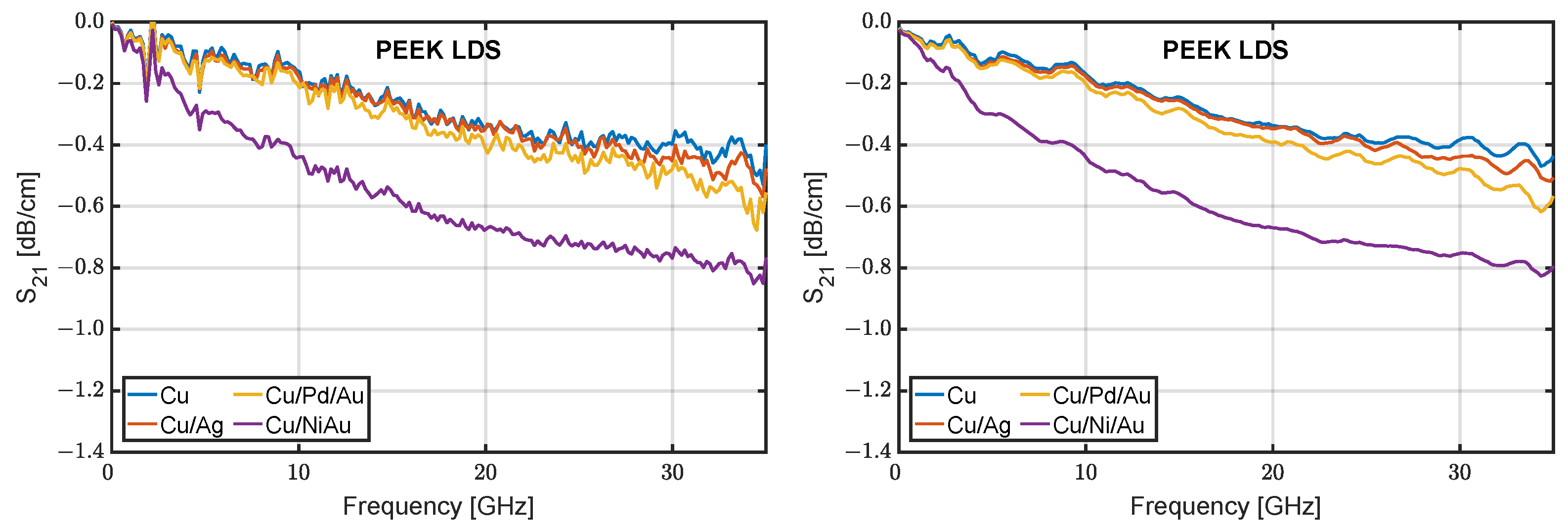
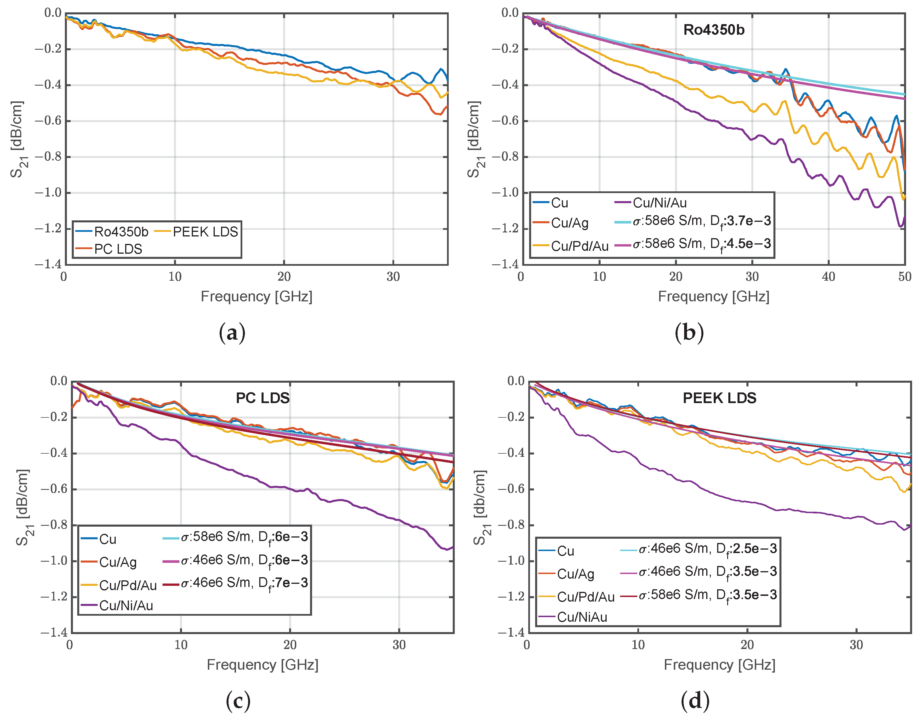
3.5. HF Charactrization of TRL-Kits

As presented, a TRL kit with a CPW transmission line was designed and fabricated on substrates of PC LDS and PEEK LDS for HF characterization. In the studies for this paper, a layout was patterned with laser parameters that minimize surface roughness. Furthermore, for the studies, different surface finishes on the copper tracks were investigated, i.e., Ni/Au, Pd/Au and Ag. For reference, a TRL kit was fabricated on a substrate made of the HF-PCB material RO4350b with the same finishes. For better visibility, the data were smoothened with a gliding mean filter to extract noise from the data. The result of the smoothening can be seen in Figure 21. Figure 22 shows the S21 measurements of the transmission lines with different surface finishes. The S21 parameter describes the insertion losses for a line normalized to a length of 1 cm. The corresponding loss values of the individual transmission lines for the 10 and 30 GHz frequency points are shown in Table 4.
In Figure 22a, the overlay of measurement curves of pure copper metallization on each of the materials is depicted. The similar trajectories of the lines show that despite their differences, the transmission lines on LDS material have similar performance to the lines on the reference material RO4350b. All measured S21 parameters are showing small ripples up to a frequency of around 30 GHz. Above this frequency, the ripples exacerbate to an ever-increasing amplitude. Those can be caused by general errors in the measurement setup. The ripples at lower frequencies are smaller for Ro4350b than for the LDS materials. One possibility for this could be the increased surface roughness of the LDS materials compared to the Ro4350b. The stronger ripples above 30 GHz are probably caused by the tapering structure at the beginning and end of the transmission line, as their length approaches 1/4 of the wavelength within the dielectric [35,36]. This is also supported by the fact that those ripples occur independent of substrate material or type of metallization. Figure 22b–d show the results for different surface finishes on Ro4350b, PC LDS and PEEK LDS as well as simulation data for different sets of bulk conductivity, dielectric loss, and metallization roughness.
Furthermore, the influence of the surface finish on the insertion loss can be seen. As expected, pure copper and Cu/Ag offer the best performance. Cu/Pd/Au leads to only minor additional losses. Only RO4350b shows slightly higher losses for the Pd/Au surface finish compared to the other materials. This can be explained by a slight overplating tendency of the Pd/Au metallization caused by slightly higher roughness in the non-metallized areas of Ro4350b compared to non-metallized LDS substrates, which disturbs the CPW line in the area of the gap between the line and the ground plane. Finally, the Ni/Au surface finish shows the highest transmission losses, which can be attributed to the electrical resistance of the nickel. As electroless plated nickel contains between 7 and 9% phosphorus, its conductivity is only about one-tenth of the bulk conductivity of pure nickel [37]. The difference between the relatively linear measurements for RO4350b and PC LDS compared to PEEK LDS is also visible, which shows a rather curved course of the S21 measurements. As the simulations provide similar trajectories, it can be deduced that this difference is caused by the specific geometric differences between the CPW lines. The simulation data additionally support the correlation between measured dielectric losses, roughness, and the assumed electrical conductivity of the deposited electroless copper, which is lower than pure copper and seems to be in the range of the electrical conductivity of gold with 4.1 10 7 S/m.

4. Discussion

While ICM is often implemented to replicate micro- and nanoscale geometries for microfluidic [38] and optical applications [39], this publication discusses the implementation of ICM for generating 3D structures in materials for electronic applications. In particular, the ICM of highly mineral-filled high-temperature thermoplastics like LCP and PEEK is not reported in the literature to the authors’ knowledge.
The replication of large recesses as analyzed in Section 3.2 shows that recesses with high wall thickness variations can be manufactured by injection–compression molding even with high-temperature thermoplastics. Large recesses in 2.5D substrates could be used to form SMD-mountable air-filled waveguide devices on PCBs, as described in [10,40]. The manufactured recesses with a depth of about 500 µm could be used to form air-filled waveguides up to a size of WR-4 (height = 0.5461 mm) [41]. Furthermore, the geometry, in combination with selective metallization, could be used to form inverted or suspended microstrip transmission lines [42]. The sack of the recesses, especially the long recesses, could be improved by further optimization of the demolding process by implementing a non-stick surface finish on the tool. An even further optimization and wall thickness decrease could be obtained by changing the process chain to overmolding of a foil.
Concepts for micromachined transmission line structures were, as mentioned above, reported by several publications [4,5,6,7,8,9,10,11,12,13]. The main benefit of trenches in the isolation gaps between signal and ground traces in CPW transmission lines is the reduction of the effective permittivity D K e f f that is experienced by transmission lines, as only a part of their electromagnetic field is concentrated in the dielectric. The authors of [6] reported a reduction of D K e f f for the even-mode and odd-mode of coupled microstrip traces. D K r e , e f f was reported to decrease from 3.081 to 2.818 and D K r o , e f f was reported to decrease from 2.463 to 2.080 for a cylindrical trench of 200 µm depth. For a conical trench, D K r e , e f f was reported to decrease from 3.094 to 3.011 and D K r o , e f f was reported to decrease from 2.510 to 2.353. This shows the decreasing E-field component in the dielectric.
LDS-MIDs offer an additional benefit to the mentioned structures. As mentioned by Lin et al. for CMOS processes, the partial metallization of trench side walls could even further improve trenched CPW lines [6]. Seewald et al. reported in [26] that the partial metallization of trench sidewalls could increase the capacitive coupling and concentrate even more field lines in the air gap, thus minimizing the losses and reducing the width of the transmission line for an LDS-MID structure. Gliese et al. reported in [43] an SMD mountable high-Q SIW mmWave filter in LDS-MID technology. Additionally, by replicating the structures from a mold, sequential milling or laser milling processes are no longer required.
In the experiments performed for this paper, the successful replication of trench geometries with a replication accuracy close to 100% over a variety of thermoplastic substrate materials on the same ICM tool was demonstrated. For PC LDS, the replication accuracies are between 95% and 103%. For LCP LDS, the range is from 99% to 101%, and for PEEK LDS, it was found to be between 98% and 101%.
PSGAs were first developed between 1996 and 2001 [27,28,29,30,31]. The publications regarding this concept mainly concentrated on the mechanical and thermal properties as well as the reliability of the interconnections rather than on the 3D geometrical aspect of the stud array.
While PSGAs were less successful for packaging ICs and were overtaken by BGA, this concept was analyzed later for usage in MIDs for mounting bare dies on MIDs [32,44,45,46] and MIDs on PCB substrates [47,48].
Kessler et al. reported in [45] on a “medial maximum height difference for an array of 20 non-metallized polymer” studs of 4.1 ± 0.3 μ m and for an array of 10 studs of 3.2 ± 0.4 μ m for a mean stud height of about 80 µm. As stated in Section 3.3, normalized to the mean stud height, the PSGA height distribution in this publication lies below these values. However, the uniformity of a stud array height distribution is mainly critical for the non-conducting adhesive (NCA) mounting processes of flip chips [32].
For other mounting processes like gluing with isotropic conductive adhesive (ICA) and soldering, this value is less important, as there is no need for full physical contact between the studs and the pads. The solder, or ICA, acts as an intermediary material and fills the gap. As the PSGAs on MIDs are mainly intended as soldering submounts on PCBs, their height distribution can be compared to solder balls as used in BGA packages. Solder ball diameter tolerances vary between ±5 µm for small diameters up to 0.15 mm and ±15 µm for balls with diameters of 0.65 and 0.76 mm.
The dielectric measurements performed show that the process changing from injection molding to injection–compression molding changes the dielectric properties of the materials only imperceptibly. Geometric analysis of the TRL-Kit and 3D structure substrates shows that the large-area wall thickness recesses to reduce RF losses in transmission lines as well as narrow trenches to reduce VIA drilling costs, and PSGAs for contacting MMICs to digital PCBs can be manufactured with low tolerances in the single-digit to low double-digit µm range. In addition, warpage measurements of the TRL kit-type parts show that the PC LDS and PEEK LDS substrates meet the maximum distortion of 0.75% required by the IPC-6012 standard, but the LCP LDS substrates exceed it. The tempering of PEEK LDS reduced the warpage, while for LCP LDS, it increased it.
The characterization of the LDS substrates proved that the roughness of the laser patterned IM and ICM substrates differed only slightly. The reason for these slight differences may be the fundamental roughness of the unstructured polymer surface. The adhesion strength of the metal layers for LCP LDS and PEEK LDS hardly changes between both manufacturing processes. Only for PC LDS were the measured adhesion strength differences significant. A possible reason for this could be an observed bending of the substrate during the hot bump pull test caused by the lower mechanical strength of the PC LDS. By placing a downholder right next to the test area, we attempted to negate this effect. While the measured adhesion strength increased from 5.7 to 6.6 N/mm 2 , a bending of the substrate was still observed. The characterization of the TRL kits on PC LDS and PEEK LDS shows comparable performance to the HF PCB substrate material RO4350b. Similar insertion loss values were reported by Friedrich et al. in [49].

5. Conclusions

In this paper, the injection–compression molding of different geometries for the utilization of LDS-MID substrates in HF applications is described. The main focus was to analyze the molding accuracy and compatibility with the LDS process. The following points can be summarized and highlighted from this study:
  • The injection–compression molding of LDS-MID substrates did not change the measured dielectric properties of the materials.
  • Injection–compression molding of LDS-MID substrates enables the precise molding of large recesses with minimized wall thicknesses for use in transmission lines or, for example, suspended patch antennas.
  • Injection–compression molding of LDS-MID substrates allows the molding of narrow trench structures for VIA optimization and stud arrays for the rerouting of BGA pads from the LDS-MIDs to an underlying substrate down to pitches of about 0.5 mm.
  • The LDS capability of LDS-MID substrates is not negatively affected by injection–compression molding. Only the increased roughness of LCP LDS can lead to an increase in metallization defects.
  • HF transmission lines with a performance comparable to that of mid-range HF PCBs can be produced on injection-molded LDS-MID substrates.

Author Contributions

Conceptualization, M.W.; methodology, M.W. and K.W.; formal analysis, M.W.; investigation, M.W.; data curation, M.W.; writing—original draft preparation, M.W. and K.W.; writing—review and editing, T.G. and W.E.; visualization, M.W.; supervision, T.G. and W.E.; funding acquisition, T.G. and A.Z.; project administration, A.Z. All authors have read and agreed to the published version of the manuscript.

Funding

This publication was funded via AiF, grant number 20668 N, within the program for promoting the Industrial Collective Research (IGF) of the Federal Ministry of Economic Affairs and Climate Action (BMWK) based on a resolution of the German Parliament. This publication was funded by the German Research Foundation (DFG) grant “Open Access Publication Funding/2023-2024/University of Stuttgart” (512689491).

Institutional Review Board Statement

Not applicable.

Informed Consent Statement

Not applicable.

Data Availability Statement

All data used are shown in the text. Raw data are available on request.

Acknowledgments

The authors would like to acknowledge the support of the BMWK.

Conflicts of Interest

The authors declare no conflict of interest.

Abbreviations

The following abbreviations are used in this manuscript:
BGABall-grid-array
CLSMVonfocal laser-scanning microscope
CPWCoplanar waveguide
DkPermittivity
DfDielectric loss factor
EMElectromagnetic
HBPHot bump pull
HFHigh frequency
IMInjection molding
ICMInjection–compression molding
LCPLiquid crystal polymer
LDSLaser direct structuring
MIDMechatronic integrated devices
MMICMonolithic microwave integrated circuit
mmWaveMillimeter wave
MPMeasuring point
PCPolycarbonate
PCBPrinted circuit boards
PEEKPoly ether ether ketone
PSGA       Polymer stud grid array
PTFEPolytetrafluoroethylene
VIAVertical interonnect access
SMDSurface-mounted devices
3DThree dimensional
5GFifth-generation technology standard for broadband cellular networks

References

  1. Ramasubramanian, K.; Ramaiah, K. Moving from legacy 24 GHz to state-of-the-art 77-GHz radar. Atzelektronik Worldw. 2018, 13, 46–49. [Google Scholar] [CrossRef]
  2. Gu, X.; Liu, D.; Sadhu, B. Packaging and Antenna Integration for Silicon-Based Millimeter-Wave Phased Arrays: 5G and Beyond. IEEE J. Microw. 2021, 1, 123–134. [Google Scholar] [CrossRef]
  3. Kirkeby, N.; Chong, M.; Buck, T. PCB Design Considerations for mmWave. Microw. J. 2022, 65, 20–32. [Google Scholar]
  4. Biurrun-Quel, C.; Teniente, J.; Del-Río, C. Reduced Loss and Prevention of Substrate Modes with a Novel Coplanar Waveguide Based on Gap Waveguide Technology. Sensors 2023, 23, 2909. [Google Scholar] [CrossRef]
  5. Yang, S.; Hu, Z.; Buchanan, N.B.; Fusco, V.F.; Stewart, J.C.; Wu, Y.; Armstrong, B.M.; Armstrong, G.; Gamble, H.S. Characteristics of trenched coplanar waveguide for high-resistivity Si MMIC applications. IEEE Trans. Microw. Theory Tech. 1998, 46, 623–631. [Google Scholar] [CrossRef]
  6. Djordjević, A.R.; Olćan, D.I.; Zajić, A.G. Modeling and design of milled microwave printed circuit boards. Microw. Opt. Technol. Lett. 2011, 53, 264–270. [Google Scholar] [CrossRef]
  7. Lin, C.P.; Jou, C.F. New CMOS-compatible micromachined embedded coplanar waveguide. IEEE Trans. Microw. Theory Tech. 2010, 58, 2511–2516. [Google Scholar] [CrossRef]
  8. Sepaintner, F.; Scharl, A.; Röhrl, F.; Bogner, W.; Zorn, S. Characterization and production of PCB structures with increased ratio of electromagnetic field in air. IEEE Trans. Microw. Theory Tech. 2020, 68, 2134–2143. [Google Scholar] [CrossRef]
  9. Park, J.H.; Baek, C.W.; Jung, S.; Kim, H.T.; Kwon, Y.; Kim, Y.K. Novel micromachined coplanar waveguide transmission lines for application in millimeter-wave circuits. Jpn. J. Appl. Phys. 2000, 39, 7120. [Google Scholar] [CrossRef]
  10. Sepaintner, F.; Scharl, A.; Jakob, J.; Keck, F.; Kunze, K.; Röhrl, F.X.; Bogner, W.; Zorn, S. Cost-effective implementation of air-filled waveguides on printed circuit boards. In Proceedings of the 2020 IEEE 29th Conference on Electrical Performance of Electronic Packaging and Systems (EPEPS), San Jose, CA, USA, 4–7 October 2020; pp. 1–3. [Google Scholar]
  11. Jang, Y.; Chun, K. Modeling of Trenched Coplanar Waveguide for Redistribution Layer of RF MEMS Switch Applications. In Proceedings of the 2018 IEEE MTT-S International Conference on Numerical Electromagnetic and Multiphysics Modeling and Optimization (NEMO), Reykjavik, Iceland, 8–10 August 2018; pp. 1–4. [Google Scholar]
  12. Llamas-Garro, I.; Corona-Chavez, A. Micromachined transmission lines for millimeter-wave applications. In Proceedings of the 16th International Conference on Electronics, Communications and Computers (CONIELECOMP’06), Puebla, Mexico, 27 February–1 March 2006; p. 15. [Google Scholar]
  13. Herrick, K.J.; Schwarz, T.A.; Katehi, L.P. Si-micromachined coplanar waveguides for use in high-frequency circuits. IEEE Trans. Microw. Theory Tech. 1998, 46, 762–768. [Google Scholar] [CrossRef]
  14. Franke, J. Three-Dimensional Molded Interconnect Devices (3D-MID); Carl Hanser Verlag: Munich, Germany, 2014. [Google Scholar]
  15. Molex-LLC. RHCP LDS SMT GPS Antenna. Available online: https://www.molex.com/en-us/part-list/antennas?taxonomyPathValueLast=Antennas&general_type=Internal&general_protocol=GPS&materialMaster_promotable=true (accessed on 15 August 2023).
  16. Kildal, S.S.; Pfuhl, N.; Flamini, R.; Biscontini, B. Molded interconnect device (MID) design for base station antenna elements. In Proceedings of the 2016 IEEE International Symposium on Antennas and Propagation (APSURSI), Fajardo, Puerto Rico, 26 June–1 July 2016; pp. 1845–1846. [Google Scholar]
  17. Chen, Y.; Zhang, C.; Lu, Y.; Yang, W.W.; Huang, J. Compact dual-polarized base station antenna array using laser direct structuring technique. IEEE Antennas Wirel. Propag. Lett. 2020, 20, 78–82. [Google Scholar] [CrossRef]
  18. Orlob, C.; Kornek, D.; Preihs, S.; Rolfes, I. Comparison of methods for broadband electromagnetic characterization of Molded Interconnect Device materials. Adv. Radio Sci. 2009, 7, 11–15. [Google Scholar] [CrossRef]
  19. Bengsch, S. Entwicklung eines Lithographiefreien Fertigungsverfahrens für AMR-Magnetfeldsensoren Basierend auf Spritzgegossenen Kunststoffsubstraten: Development of a Lithography-Free Manufacturing Process for AMR Magnetic Field Sensors Based on Injection-Molded Plastic Substrates; TEWISS Verlag: Garbsen, Germany, 2022. [Google Scholar]
  20. Mitsubishi Engineering Plastics Corp. XANTAR LDS 3760® LDS 3760; Mitsubishi Engineering Plastics Corp.: Tokyo, Japan, 2017. [Google Scholar]
  21. Ensinger GmbH. TECACOMP® LCP LDS Black 4107; Ensinger GmbH: Nufringen, Germany, 2016. [Google Scholar]
  22. Ensinger GmbH. TECACOMP® PEEK LDS Black 1047045; Ensinger GmbH: Nufringen, Germany, 2019. [Google Scholar]
  23. Rogers Corp. RO4000 Series High Frequency Circuit Materials Data Sheet; Rogers Corp.: Chandler, AZ, USA, 2022. [Google Scholar]
  24. AGC Inc. TSM-DS3 Dimensionally Stable Low Loss Laminate; AGC Inc.: Amagasaki, Japan, 2022. [Google Scholar]
  25. Wolf, M.; Werum, K.; Guenther, T.; Schleeh, L.; Eberhardt, W.; Zimmermann, A. Analysis of Tempering Effects on LDS-MID and PCB Substrates for HF Applications. J. Manuf. Mater. Process. 2023, 7, 139. [Google Scholar] [CrossRef]
  26. Seewald, S.; Manteuffel, D.; Wolf, M.; Barth, M.; Eberhardt, W.; Zimmermann, A. Low-Loss 3D-Coplanar Line Structure for Millimeter Wave Applications Using Laser Direct Structuring Technology. In Proceedings of the 2021 International Conference on Electromagnetics in Advanced Applications (ICEAA), Honolulu, HI, USA, 9–13 August 2021; p. 85. [Google Scholar]
  27. Christiaens, F.; Beyne, E.; Vandevelde, B.; Roggen, J.; Mertens, R.P.; Berghmans, J. Thermal Modelling of the Polymer Stud Grid Array (PSGA) Packages. Int. J. Microcircuits Electron. Packag. 1997, 20, 521–531. [Google Scholar]
  28. Wojciechowski, D.; Chan, M.; Martone, F. Lead-free plastic area array BGAs and polymer stud grid arraysTM package reliability. Microelectron. Reliab. 2001, 41, 1829–1839. [Google Scholar] [CrossRef]
  29. Chandrasekhar, A.; Vandevelde, B.; Driessens, E.; Beyne, E.; De Raedt, W.; Pieters, P.; Nauwelaers, B.; Van Puymbroeck, J. Modeling and characterization of the polymer stud grid array (PSGA) package: Electrical, thermal and thermo-mechanical qualification. IEEE Trans. Electron. Packag. Manuf. 2003, 26, 54–67. [Google Scholar] [CrossRef]
  30. Driessens, E.; Van Dooren, S.; Vandevelde, B.; Degryse, D.; Beyne, E.; Heerman, M.; Van Puymbroeck, J. Parametric compact models for the 72-pins polymer stud grid array™. Microelectron. J. 2001, 32, 839–846. [Google Scholar] [CrossRef]
  31. Wegener, C. Polymer Stud Grid Array (PSGA) A new 3D-Package Technology for Ball-Grid Array and Chip Scale Packaging-Applications. In Proceedings of the 5th International Congress Molded Interconnect Devices, Erlangen, Germany, 27–28 September 2000. [Google Scholar]
  32. Kessler, U. Untersuchungen zur Flip Chip Montage auf Spritzgegossenen Schaltungsträgern; Ingenieurwissenschaften, Verl. Dr. Hut GmbH: München, Germany, 2012. [Google Scholar]
  33. Domininghaus, H.; Elsner, P.; Eyerer, P.; Hirth, T. (Eds.) Einführung in Polymer Engineering. In Kunststoffe: Eigenschaften und Anwendungen; Springer: Berlin/Heidelberg, Germany, 2008; pp. 1–161. [Google Scholar] [CrossRef]
  34. Keysight Technologies. Solutions for Measuring Permittivity and Permeability with LCR Meters and Impedance Analyzers; Keysight Technologies: Santa Rosa, CA, USA, 2014. [Google Scholar]
  35. Schmückle, F.; Doerner, R.; Phung, G.; Heinrich, W.; Williams, D.; Arz, U. Radiation, multimode propagation, and substrate modes in W-band CPW calibrations. In Proceedings of the 2011 41st European Microwave Conference, Manchester, UK, 10–13 October 2011; pp. 297–300. [Google Scholar]
  36. Spirito, M.; Gentile, G.; Akhnoukh, A. Multimode analysis of transmission lines and substrates for (sub)mm-wave calibration. In Proceedings of the 82nd ARFTG Microwave Measurement Conference, Columbus, OH, USA, 18–21 November 2013; pp. 1–6. [Google Scholar] [CrossRef]
  37. Parkinson, R. Properties and Applications of Electroless Nickel; Nickel Development Institute: Durham, NC, USA, 2001. [Google Scholar]
  38. Attia, U.; Marson, S.; Alcock, J. Micro-injection moulding of polymer microfluidic devices. Microfluid. Nanofluidics 2009, 7, 1–28. [Google Scholar] [CrossRef]
  39. Kang, S. Replication Technology for Micro/Nano Optical Components. Jpn. J. Appl. Phys. 2004, 43, 5706. [Google Scholar] [CrossRef]
  40. Huegel, U.; Garcia-Tejero, A.; Glogowski, R.; Willmann, E.; Pieper, M.; Merli, F. 3D Waveguide Metallized Plastic Antennas Aim to Revolutionize Automotive Radar. Microw. J. 2022, 65, 32–48. [Google Scholar]
  41. IEEE Standard for Rectangular Metallic Waveguides and Their Interface for Frequencies of 110 GHz and Above—Part 1: Frequency Bands and Waveguide Dimensions, Standard 1785.1-2012. pp. 1–20. Available online: https://ieeexplore.ieee.org/document/7564020 (accessed on 20 September 2023).
  42. Bahl, I.; Bozzi, M.; Garg, R. Microstrip Lines and Slotlines, 3rd ed.; Horizon House Publications: Norwood, MA, USA, 2013. [Google Scholar]
  43. Glise, A.; Quéré, Y.; Maalouf, A.; Rius, E.; Castel, V.; Laur, V.; Sauvage, R. LDS Realization of High-Q SIW Millimeter Wave Filters with Cyclo-Olefin Polymers. Appl. Sci. 2018, 8, 2230. [Google Scholar] [CrossRef]
  44. Hahn-Schickard-Gesellschaft für angewandte Forschung e.V. Untersuchungen zur Einsetzbarkeit der Flipchip-Technik für die Kontaktierung von Nacktchips in Niniaturisierten MID-Gehäusen in der Mikrosystemtechnik. 2004. Available online: https://www.aif.de/foerderangebote/igf-industrielle-gemeinschaftsforschung/igf-projektdatenbank.html?tx_igf_search%5Baction%5D=detail&tx_igf_search%5Bcontroller%5D=Search&tx_igf_search%5Bitem%5D=3282&tx_igf_search%5Bterm%5D=Untersuchungen%20zur%20Einsetzbarkeit%20der%20Flipchip-Technik&cHash=6afaa9cfb238a52f0dd02a7ccb4b250d (accessed on 4 October 2023).
  45. Kessler, U.; Eberhardt, W.; Schwenck, A.; Warkentin, D.; Kuck, H. Properties of Polymer Bumps for Flip Chip Mounting on Moulded Interconnect Devices(MID). In Proceedings of the 2006 1st Electronic Systemintegration Technology Conference, Dresden, Germany, 5–7 September 2006; Volume 1, pp. 287–290. [Google Scholar] [CrossRef]
  46. Kessler, U.; Kuck, H.; Eberhardt, W. Technology for flipchip assembly on moulded interconnect devices (MID). In Proceedings of the 6th IEEE CPMT Conference on High Density Microsystem Design and Packaging and Component Failure Analysis (HDP ’04), Shanghai, China, 30 June–3 July 2004; pp. 242–247. [Google Scholar] [CrossRef]
  47. Hahn-Schickard-Gesellschaft für angewandte Forschung e.V. Simulationsunterstützte Auslegung von Kontaktelementen zur SMT-Kompatiblen Montage von 3D-MID Packages auf Leiterplatten. 2011. Available online: https://www.aif.de/foerderangebote/igf-industrielle-gemeinschaftsforschung/igf-projektdatenbank.html?tx_igf_search%5Baction%5D=detail&tx_igf_search%5Bcontroller%5D=Search&tx_igf_search%5Bitem%5D=6259&tx_igf_search%5Bterm%5D=Simulationsunterst%C3%BCtzte%20Auslegung%20von%20Kontaktelementen%20zur&cHash=07a79ab114cc6667584cffedfac56f7a (accessed on 4 October 2023).
  48. Hahn-Schickard-Gesellschaft für Angewandte Forschung e.V.Untersuchungen zur Porenbildung in Bleifreien SAC-Lötverbindungen auf LDS-MID. 2014. Available online: https://www.aif.de/foerderangebote/igf-industrielle-gemeinschaftsforschung/igf-projektdatenbank.html?tx_igf_search%5Baction%5D=detail&tx_igf_search%5Bcontroller%5D=Search&tx_igf_search%5Bitem%5D=7910&tx_igf_search%5Bterm%5D=Untersuchungen%20zur%20Porenbildung%20in%20Bleifreien%20SAC-L%C3%B6tverbindungen&cHash=5d577529a8c7f15e504f013858cee28a (accessed on 4 October 2023).
  49. Friedrich, A.; Geck, B.; Fengler, M. LDS manufacturing technology for next generation radio frequency applications. In Proceedings of the 2016 12th International Congress Molded Interconnect Devices (MID), Wuerzburg, Germany, 28–29 September 2016; pp. 1–6. [Google Scholar] [CrossRef]
Figure 1. Concept of a LDS-MID submount for HF applications.
Jmmp 07 00184 g001
Figure 2. Part designs for injection–compression molding: disc 1—TRL kit (top), disc 2—trenches and studs (bottom).
Jmmp 07 00184 g002
Figure 3. TRL kit for CPW transmission line.
Jmmp 07 00184 g003
Figure 4. Results of dielectric characterization of PC LDS, LCP LDS and PEEK LDS substrates fabricated by IM and ICM processes measured by capacitance method at 1 GHz.
Jmmp 07 00184 g004
Figure 5. Left: Three-dimensional (3D) image of a measured cavity step of a disc 1 PEEK LDS substrate; Right: step height and inclination angle data from CLSM measurements.
Jmmp 07 00184 g005
Figure 6. Tactile thickness measurement data of disc 1.
Jmmp 07 00184 g006
Figure 7. Measurement positions of mechanical thickness measurements.
Jmmp 07 00184 g007
Figure 8. Cross-section of PEEK LDS ICM substrate within cavity.
Jmmp 07 00184 g008
Figure 9. Maximal warpage of TRL-type LDS-MID substrates from PC LDS, LCP LDS and PEEK LDS. The error bars indicate the minimal warpage of all measured LDS-MID substrates.
Jmmp 07 00184 g009
Figure 10. Sideview of untempered and tempered LCP LDS (top) and PEEK LDS (bottom) disc 1 substrates.
Jmmp 07 00184 g010
Figure 11. Comparison of differences between (a) ICM stamper and tempered disc 1 PEEK LDS substrate, (b) untempered and tempered disc 1 PEEK LDS substrates, and (c) two-tempered disc 1 PEEK LDS substates.
Jmmp 07 00184 g011
Figure 12. Measurement data of maximal height differences within recesses on disc 1 LDS substrates.
Jmmp 07 00184 g012
Figure 13. Three-dimensional (3D) view of trenches manufactured in PEEK LDS by ICM.
Jmmp 07 00184 g013
Figure 14. Trench depth of ICM specimen measured by structured light projection method. The error bars indicate the minimal height difference of all measured LDS-MID substrates of a given material.
Jmmp 07 00184 g014
Figure 15. Picture of a PSGA made by CLSM.
Jmmp 07 00184 g015
Figure 16. Mean PSGA array heights measured by the structured light projection method.
Jmmp 07 00184 g016
Figure 17. Mean span of measured PSGA height normalized by mean PSGA height σ Δ ¯ m a x m i n / x ¯ with additional data points as reference from [32].
Jmmp 07 00184 g017
Figure 18. Surface defects on LCP LDS, (a) 3D view of surface displacements, (b) 3D height representation of surface defects in LCP LDS, (c) metallization defects on LCP LDS, and (d) optimal metallization on PEEK LDS.
Jmmp 07 00184 g018
Figure 19. Roughness measurements of LDS-MIDs manufactured by IM and ICM on non-structured, structured and metallized areas.
Jmmp 07 00184 g019
Figure 20. Adhesion strength of LDS-MIDs manufactured by IM and ICM.
Jmmp 07 00184 g020
Figure 21. Smoothening of raw measurement data by the moving average method. Left: raw data of a measurement of a CPW line with different surface finish on PEEK LDS, right: smoothened measurement curve.
Jmmp 07 00184 g021
Figure 22. S-parameter measurements and simulation data of CPW transmission lines on Ro4350b, PC LDS and PEEK LDS for different metallizations; (a) CPW transmission lines with copper metallization on all materials used; (b) CPW transmission lines on RO4350b; (c) CPW transmission lines on PC LDS; (d) CPW transmission lines on PEEK LDS.
Jmmp 07 00184 g022
Table 1. Nominal dimensions of stud arrays on disc 2.
BGA PitchBump Array TypePSGA Bottom Diameter (mm)PSGA Top Diameter (mm)PSGA Height (mm)
0.8 mmStandard0.500.25268
Double Pitch10.75
Elongated dim 12.0/0.51.75/0.25
Elongated dim 21.2/0.50.95/0.25
0.65 mmStandard0.40.2214
Double Pitch0.80.6
Elongated dim 11.625/0.41.425/0.2
Elongated dim 20.975/0.40.775/0.2
0.5 mmStandard0.30.15125
Double Pitch0.60.45160
Elongated dim 11.25/0.31.1/0.15
Elongated dim 20.75/0.30.6/0.15
Table 2. ICM parameter set used.
ParameterPC LDSLCP LDSPEEK LDS
Disc 1 Disc 2 Disc 1 Disc 2 Disc 1 Disc 2
Injection temperature ( C)290290350340420420
Mold temperature ( C)100100100140180180
Injection pressure (MPa)250250250250250250
Holding pressure (MPa)7.51252,58015,5225
Injection time (s)0.180.160.150.160.150.16
closing delay (s)0.180.160.150.160.150.16
Compression force (kN)200200200200200200
Compression time (s)333333
Compression path (mm)0.060.060.060.060.100.06
Table 3. Mean maximum spanns for PSGAs in micrometer.
PitchArray TypeNumber of StudsPC LDSLCP LDSPEEK LDS
Δ ¯ max min σ Δ ¯ max min Δ ¯ max min σ Δ ¯ max min Δ ¯ max min σ Δ ¯ max min
0.8 mmstd486.92.418.73.511.43.4
long1616.61.911.31.98.40.8
double124.80.54.91.45.41
0.65 mmstd4810.03.017.26.813.31.4
long169.92.012.43.014.30.9
double121.50.24.31.33.50.8
0.5 mmstd484.21.810.52.85.21.4
long1612.11.09.71.115.11.4
double121.90.36.01.43.81.4
Table 4. S21 values at 15 and 30 GHz of characterized TRL kits on Ro4350b, PC LDS and PEEK LDS.
S 21 in [dB/cm]
Ro4350b PC LDS PEEK LDS
@ 15 GHz @ 30 GHz @ 15 GHz @ 30 GHz @ 15 GHz @ 30 GHz
Cu−0.13−0.35−0.16−0.42−0.16−0.40
Cu/Ag−0.14−0.35−0.16−0.38−0.18−0.45
Cu/Pd/Au−0.22−0.55−0.20−0.35−0.21−0.48
Cu/Ni/Au−0.28−0.71−0.34−0.77−0.44−0.77
Disclaimer/Publisher’s Note: The statements, opinions and data contained in all publications are solely those of the individual author(s) and contributor(s) and not of MDPI and/or the editor(s). MDPI and/or the editor(s) disclaim responsibility for any injury to people or property resulting from any ideas, methods, instructions or products referred to in the content.

