Article

Fabrication of Punch and Die Using Plasma-Assisted 3D Printing Technology for Piercing Sheet Metals

1
Surface Engineering Design Laboratory, Shibaura Institute of Technology, Tokyo 144-0045, Japan
2
Komatsu-Seiki Kosakusho, Co., Ltd., Suwa 392-0012, Japan
3
Faculty of Engineering, University of Toyama, Toyama 930-8555, Japan
*
Author to whom correspondence should be addressed.
J. Manuf. Mater. Process. 2022, 6(3), 49; https://doi.org/10.3390/jmmp6030049
Submission received: 27 February 2022 / Revised: 8 April 2022 / Accepted: 9 April 2022 / Published: 20 April 2022

Abstract

:
A pair of punch and die was often fabricated using subtractive manufacturing processes such as milling and other machining processes. However, additive manufacturing could be used to perform the same processes. This study explored this possibility. In particular, this study fabricated a pair of T-shaped punch and die made of AISI316L austenitic stainless steel using an additive manufacturing process called plasma-assisted 3D printing. Accordingly, T-shaped negative and positive 2D patterns were screen-printed onto the mirror-polished surfaces of the substrates made of AISI316L austenitic stainless steel. The printed film worked like a mask to prevent the printed substrate surfaces from nitriding. In order to form a thick nitrided layer, the unprinted substrate surfaces were selectively nitrided at 673 K for 14.4 ks. The un-nitrided segments of the substrates were uniformly removed by sand-blasting that involved shooting silica particles on the substrate’s surfaces. As a result, the substrates printed with negative and positive T-shaped patterns were transformed into the punch head and die cavity. In order to see the efficacy of the fabricated punch and die pair, this pair was used for piercing the electrical steel sheets under a controlled clearance. Scanning Electron Microscopy with Energy Dispersive X-ray (SEM-EDX) was used to measure surface topography after piercing. In addition, SEM and a 3D profilometer were used to measure the punch and die profiles after piercing. The abovementioned measurement results showed that the fabricated punch and die exhibited highly accurate piercing behavior. Thus, the plasma-assisted 3D printing was useful for punch and die fabrication.

1. Introduction

Mold and die technologies have paralleled advancements in subtractive manufacturing processes (mechanical machining and milling). Precise tooling provided a solution to fabricate complex-shaped punches and dies for stamping and forging [1]. With the down-sizing of products, however, this solution only stands for long tact-time productions to build up CAM (Computer Aided Machining) data for a large amount of tooling paths for cutting, for the positioning control of cutting tools, and for preserving tool life by heat treatment and surface modification [2]. Hence, alternative methods are necessary to significantly shorten this tact time with the lessened use of mechanical machining and milling as well as additional treatments. The first candidate method is short-pulse laser machining without the use of cutting tools. This solution provided a method for micro-/nano-texturing processes to be free from shortened tool life [3,4]. A significant amounts of CAM data are still necessary to determine the laser machining paths on well-defined cutting planes. Additive manufacturing or 3D-printing [5,6] is the second approach to prepare the necessary CAM data for manufacturing by algorithmic deductions from the product model. Although the tact time is much reduced without preparations for CAM data, mechanical milling is needed for shaping and finishing the additively constructed surfaces of products [6]. In particular, punch/die edges and their side surfaces must be precisely formed by mechanical milling [7]. In addition, the rough surfaces of additively shaped dies must be polished and adjusted within the engineering tolerances of roughness [8]. Furthermore, heat and surface treatments are indispensable to increase the hardness of reshaped stainless steel dies from the sintered die substrate in additive manufacturing [9].
The third approach was plasma printing without the use of mechanical machining as well as CAM data for cutting [10]. In plasma printing, the punch head geometry was printed as a two-dimensional pattern onto the die substrate surface by using ink-jet printing [11], screen printing [12], and maskless lithography [13], respectively. This substrate with the printed pattern was nitrided at low temperature with the assistance of plasmas; e.g., AISI316 and AISI420 stainless steels were plasma nitrided at 673 K for 14.4 ks to possess higher nitrogen solute content than 4 mass% on average within the nitrided layer [14]. Afterward [14,15,16], this low temperature plasma nitriding process was characterized by nitrogen supersaturation with high nitrogen solute concentrations into the depth of the matrix without the precipitation of nitrides. During this process plasma nitriding, the printed micropattern on the die surface worked as a mask to prevent the printed substrate surface from nitriding. This selective nitriding through the unprinted surface resulted in the selective hardening of die materials. Afterward [11,12,13], the unprinted die had a hardness higher than 1000 HV, while the printed surface hardness remained the same as the substrate matrix’s hardness. Hence, the hardened and chemically stabilized punch was automatically fabricated by the mechanical removal of the printed part from the nitrided substrate or by chemically etching it [17,18]. This selective nitrogen supersaturation and hardening plays a key role in plasma printing. Plasma printing was effective to fabricate embossing or micro-embossing punches with a tailored punch head array by CAD (Computer Aided Design) and yielded embossed and micro-embossed products by imprinting [11,12]. Otherwise, plasma printing failed by itself even by using metallic masks; no punch heads and die cavities were fabricated in [19].
In die technologies for fine piercing of electrical steel sheets or micro-piercing of copper alloy connectors [20], several issues remained unsolved in plasma printing. A pair of punch and die must be plasma-printed with the same accuracy in dimension as each other. The punch’s height and the die’s cavity depth must be more than the work sheet’s thickness; these are necessary conditions to punch out the T-shaped motor core sheet unit. The clearance between the punch and die profiles must be homogeneously fixed within engineering tolerances. The punch and die edges have to be sharpened to shear out electrical steel sheets.
In the present paper, original plasma printing processes are advanced to fabricate punches and dies simultaneously for finely piercing electrical steel sheets without the use of mechanical machining and milling, as well as heat treatment. The present plasma-assisted 3D-printing procedure consists of three steps: (1) screen printing of masking patterns onto the die substrates, (2) selectively plasma nitriding them, and (3) mechanically removing screen-printed surface areas by sandblasting. By using this three-step procedure, the original CAD data for punch head and die cavity transform is used for the actual T-shaped piercing punch and die, respectively, in terms of geometry without the use of mechanical machining and milling. The punch’s height and die’s cavity depth are precisely measured by a three-dimensional profilometer to prove that sufficient height and depth for piercing is attained by plasma printing. SEM (Scanning Electron Microscopy)–EDX (Electron Dispersive X-ray spectroscopy) is utilized to describe the selective nitriding behavior exhibited through the unmasked surface area. The nitrided layer in the punch and die has sufficient hardness and strength by nitrogen supersaturation, which is sufficient to function as piercing die units without the additional use of heat treatment. This pair is fixed into a cassette die set for finely piercing electrical steel sheets by using the CNC (Computer Numerical Control) stamping system. The T-shaped motor-core sheet unit is punched out from the electrical steel sheet with less burrs and slight shear droops. The burnished surface area reaches 70% of sheet thickness. This piercing behavior demonstrates that the actual clearance between the punch and die profiles is properly fixed in the piercing process.

2. Experimental Procedure

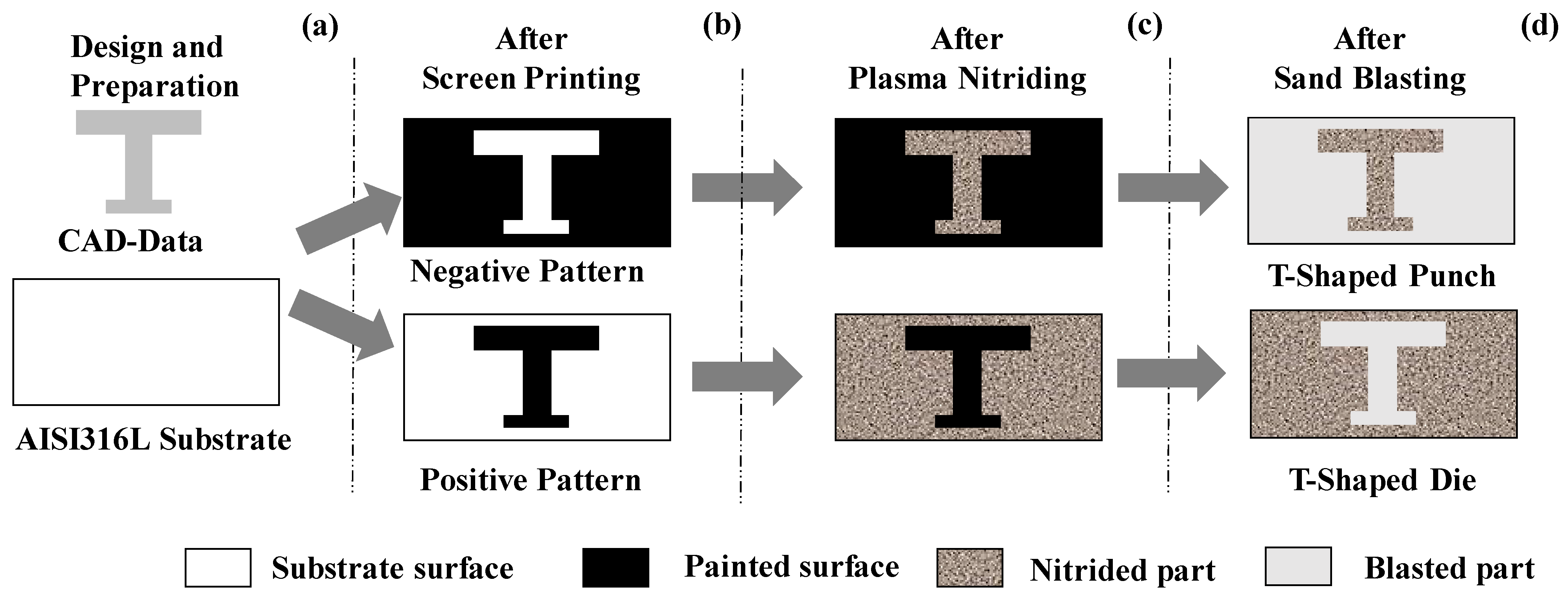
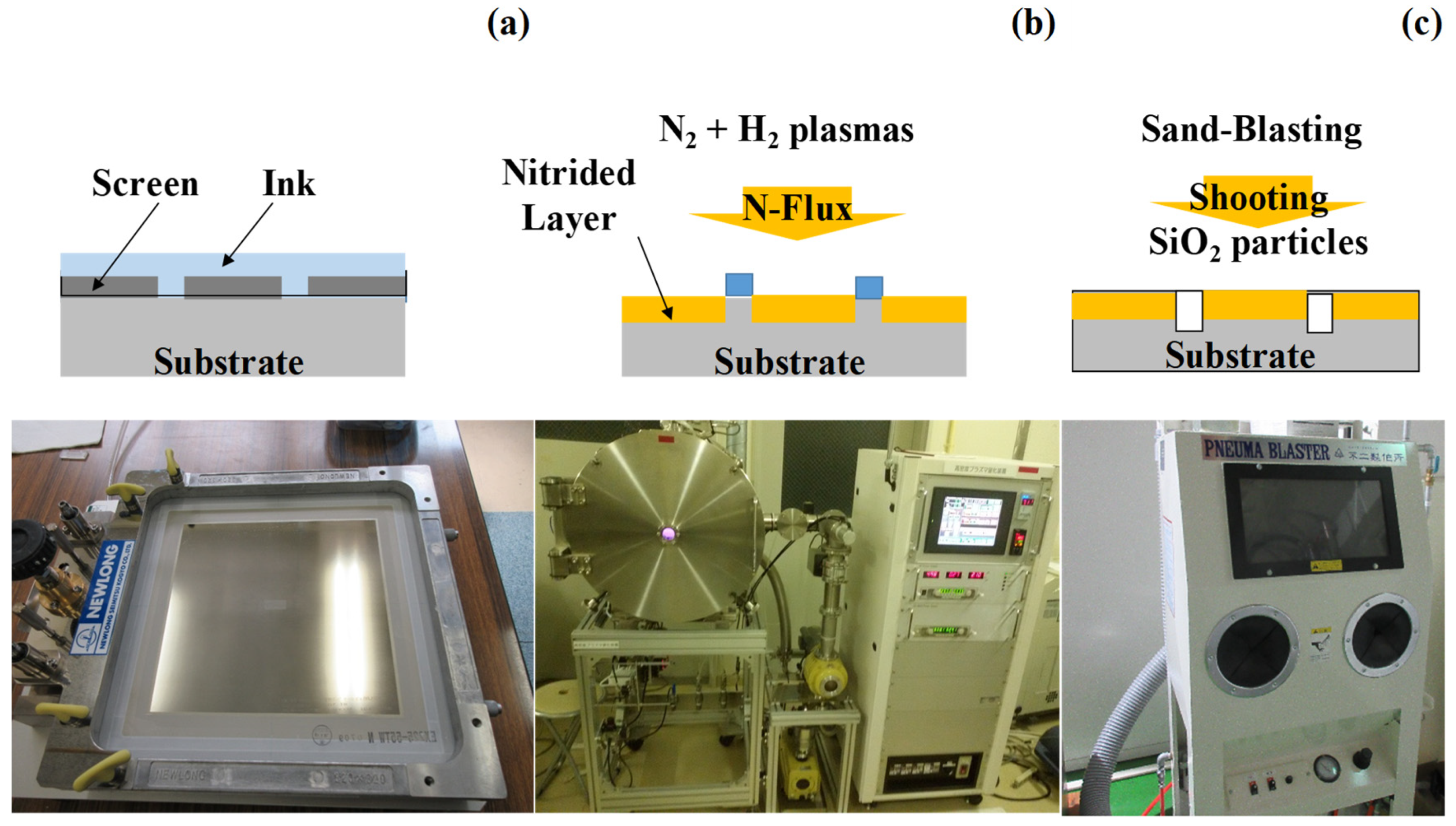
2.1. Plasma-Assisted 3D-Printing Procedure

The plasma-assisted 3D-printing procedure is used to fabricate the T-shaped punch and die for piercing a T-shaped motor-core electrical steel sheet unit. Figure 1 schematically depicts the three step procedure.
Both printing processes to build up the T-shaped punch and die start from the preparation of AISI316L substrate with a mirror-polished surface, as illustrated in Figure 1a. In the first step, a screen film is made from CAD data of the T-shaped motor-core unit to print the micropattern onto each substrate surface. A T-shaped micropattern is printed in the negative form to fabricate a T-shaped piercing punch head and in the positive form to fabricate the T-shaped cavity of the die, as shown in Figure 1b, respectively. These two screen-printed substrates are plasma nitrided to induce selective nitrogen supersaturation to the unprinted substrate surfaces. As shown in Figure 1c, the unprinted surface of substrate is selectively nitrided; the printed one is masked by the printed ink to be free from nitriding. By plasma nitriding, the unprinted part of AISI316L substrate is nitrogen supersaturated with much higher nitrogen solute contents than the maximum nitrogen solubility of 0.1 mass% for austenitic stainless steels [11,12,13]. On the other hand, its printed substrate remains as an austenitic stainless-steel matrix without nitrogen solutes. The nitrided AISI316L substrate with a negatively printed micropattern has much higher hardness only in the T-shaped region than matrix hardness. On the other hand, the substrate with the positively printed micropattern is selectively nitrided to have higher hardness in other parts than the T-shaped region. In the third step, sand-blasting with the use of silica particles as a shooting medium is used to mechanically remove the lower hardness parts of dies than the silica hardness of 700 HV. The un-nitrided parts with the matrix hardness of AISI316L in these two substrates are automatically removed by this mechanical blasting. As a result, the nitrided and hardened punch with the T-shaped head is formed from the negatively patterned substrate and the nitrided and hardened die with a T-shaped cavity is also fabricated from the positively patterned substrate, as illustrated in Figure 1d. Selective nitriding is reflected on the hardness profile, which is discussed later. The border between screen-printed and unprinted areas determines the punch and die edge configurations.
The plasma-assisted 3D-printing method used three facilities, as depicted in Figure 2. In screen-printing, two screens were prepared and set alternatively to the printer (NEWLONG, Co., Ltd., Shinagawa, Tokyo, Japan) in Figure 2a to print negative and positive micropatterns onto AISI316L substrate surfaces with the size of 10 mm × 20 mm, respectively. In the plasma nitriding step, two printed substrates were placed in the hollow cathode setup to attain the high nitrogen ion density in the order of 3 × 10¹⁷ ions/m3 at 70 Pa after presputtering [14,21]. The plasma nitriding system (YS-Electric Industry, Co., Ltd., Yamanashi, Japan) was depicted in Figure 2b. The screen-printed die substrates were nitrided at 673 K for 14. 4 ks at 70 Pa using a nitrogen–hydrogen mixture gas with a flow rate ratio of 160 mL/min for nitrogen and 30 mL/min for hydrogen. Input–output power balancing was automatically matched by the adjustment of frequency in RF (Radio Frequency) around 2 MHz. RF and DC (Direct Current) voltages were constant by 250 V and −500 V, respectively. After cooling down in the chamber and after performing evacuation, two substrates were polished for 600 s by ultrasonic cleansing. Figure 2c depicts the blasting apparatus used for manual operation. Two nitrided substrates were sandblasted manually by the blasting system (Fuji Manufacturing Co., Ltd., Edogawa, Tokyo, Japan) to selectively remove un-nitrided parts with printed ink masks from the substrates. Due to the significant difference in hardness between the printed and unprinted surface areas, the un-nitrided areas were completely removed by during this process. The blasting rate was controlled by the shooting speed of the blasting media. The punch’s height and die-cavity depths were varied by blasting duration. In the following blasting process, fine silica particles with an average diameter of 5 μm were utilized as a blasting medium. The shooting rate was constant by 2 m/s; the shooting angle was 60°. The specimen was fixed into a jig on the stage for continuous shooting operations. The duration was selected to be 600 s for deep blasting into the un-nitrided part of the substrates.

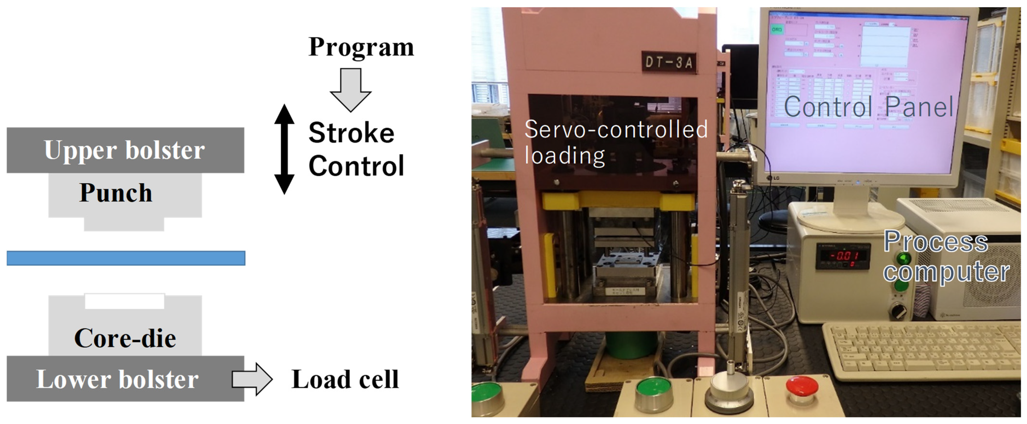
2.2. Piercing Experimental Procedure

The as-blasted punch and die were adjusted in terms of dimensions by polishing. Then, they were fixed into the upper and lower cassette die-sets, respectively. Figure 3 depicts the CNC stamping system (Fine Metal Forming Laboratory, LLC.; Tokyo, Japan) for piercing experiments. Those cassette die-sets were, respectively, cemented at the upper and lower bolsters in this system. The loading schedule was controlled by the stroke sequence. The maximum load was 50 kN. The load cell was embedded into the lower cassette die-set to in situ monitor the load–stroke relationship.

3. Experimental Results

The AISI316L punch and die with a T-shaped head and cavity were fabricated by the plasma-assisted 3D-printing procedure. SEM, EDX, and a three-dimensional profilometer were utilized to describe the selective nitrogen supersaturation process and to evaluate the dimensional accuracy of the punch’s head and core-die cavity. An unoriented Fe-6Si electrical steel sheet with a thickness of 200 μm was used for the piercing experiment.

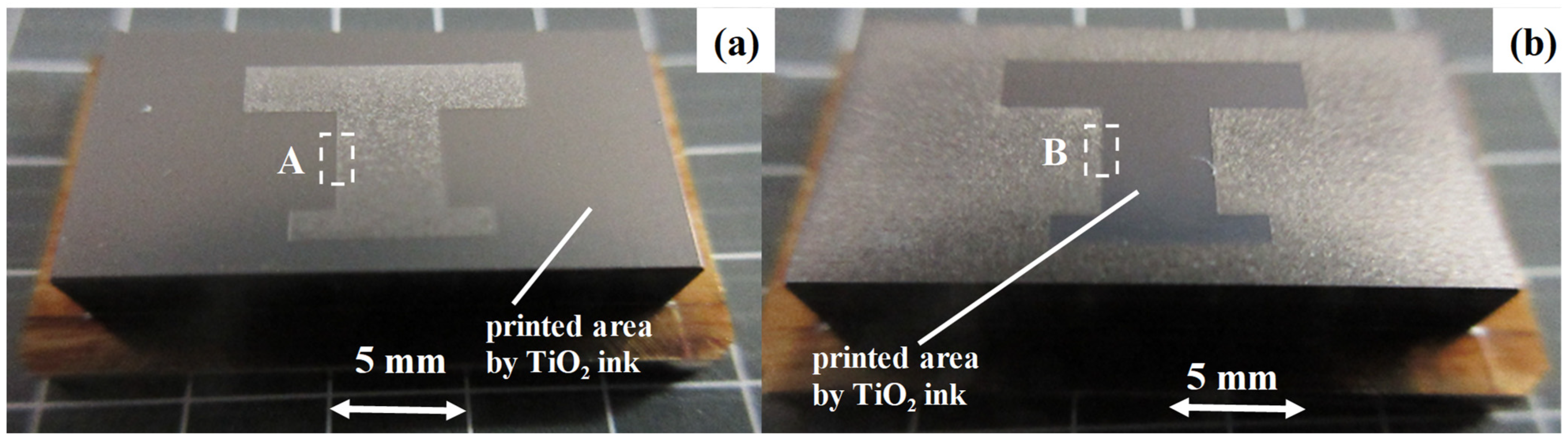
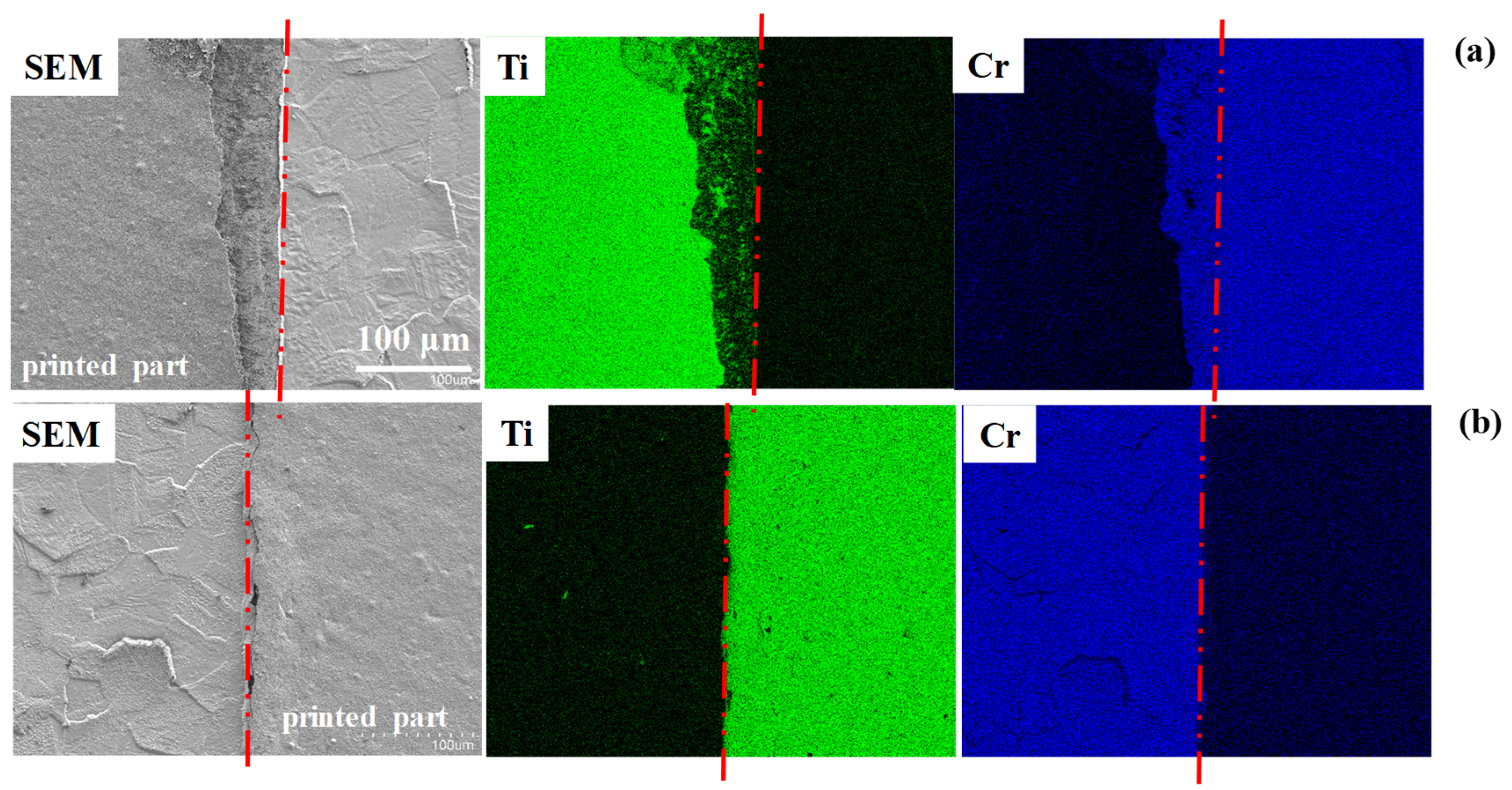
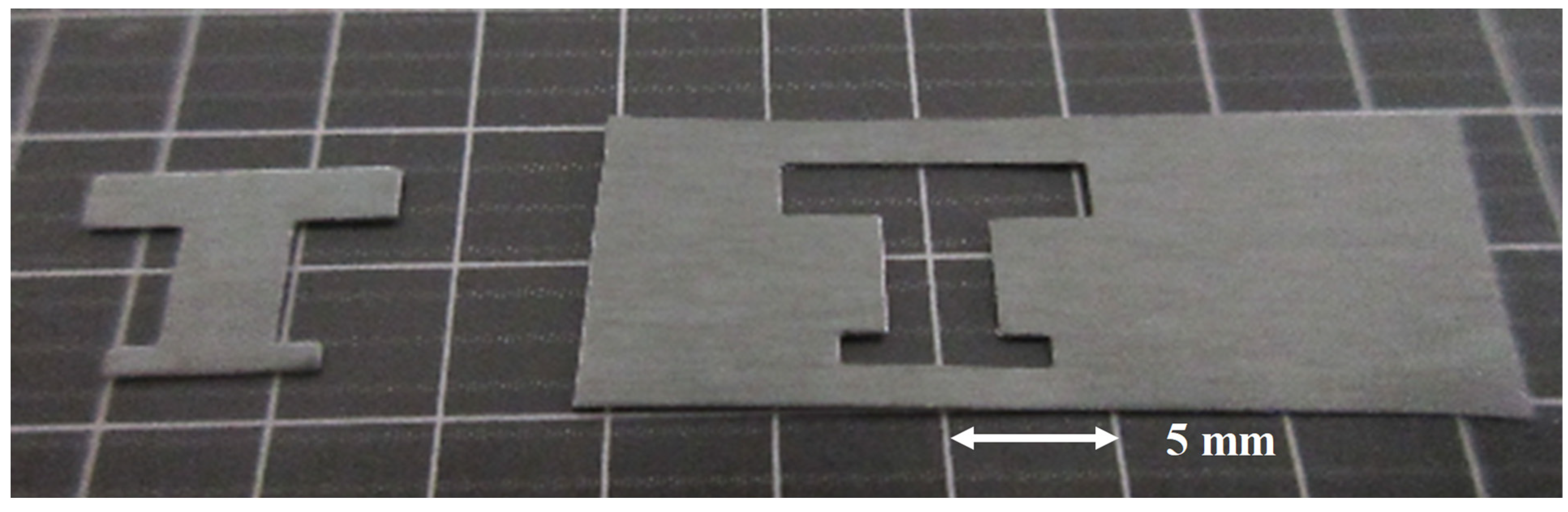
3.1. Screen Printing of Positive and Negative Micropatterns onto the Die Substrate Surfaces

Two screen films were prepared to print negative and positive patterns onto the T-shaped motor-core sheet unit onto the AISI316L substrates. In this screen-printing process, every pattern on the film is directly printed onto any flat or curved surface of plates and solids by using TiO2 ink with a polymer solvent. When using the negative-patterned film relative to the T-shaped sheet unit, the entire substrate surface other than this T-shaped geometry is masked by ink, as depicted in Figure 4a. On the other hand, when using the positive-patterned film, the T-shaped pattern is directly printed onto the AISI316L substrate surface, as shown in Figure 4b. After printing, these substrates were dried and treated at 473 K to solidify the printed mask. No significant shrinkages and expansion of inks were detected after this hot-drying process. These hot-dried patterns had sufficient heat resistance at the holding temperature in the following plasma nitriding process [11,12,13].

3.2. Selective Nitrogen Supersaturation to Unprinted Surfaces

These micropatterned die substrates were plasma nitrided at 673 K for 14.4 ks to conduct the selective nitriding of unprinted surfaces. Figure 5 depicts the optical microscopy images on the nitrided die substrates with the screen-printed micropatterns relative to T-shaped geometry. As shown in Figure 5a, the T-shaped region has a dull, rough surface, while the other parts are still covered by the printed mask. As depicted in Figure 5b, when exchanging the negative micropattern with the positive one in screen-printing, the T-shaped region is only covered by a dark-colored mask, and the others have a dull surface similarly to the T-shaped region in Figure 5a. In correspondence to the negative or positive micropatterns in Figure 4, the T-shaped region is selectively nitride, and the others are exclusively never nitrided in Figure 5a. The T-shaped region is selectively never nitrided, and the others are exclusively nitrided in Figure 5b. This exclusive nitriding behavior is described by SEM–EDX analysis.
Figure 6 compares the element mapping and microstructure between the A-region in Figure 5a and the B-region in Figure 5b. SEM image at A-region in Figure 6a shows that microstructure changes drastically at the border between unprinted and printed zones or between nitrided and un-nitrided zones. The titanium-only sample is distributed on the printed zones, which are fully covered by TiO2 ink to prevent nitrogen diffusion. On the other hand, chromium is detected only in the unprinted zones. At the B-region in Figure 6b, the element mapping of titanium and chromium becomes inverse relative to each mapping in the A-region in Figure 6a. The nitrided AISI316L substrate in Figure 5b was cut in half to investigate the microstructure and element mapping in the depth across the border between the unprinted and printed zones or between the nitrided and un-nitrided regions, as shown in Figure 7a,b, respectively. Figure 7c depicts the element mapping of N, Cr, Ti, and Si. Both Ti and Si were present on the surface of the printed region; these elements only came from TiO2 ink. On the other hand, Cr was homogeneously distributed on the cross-section, except for the surface of the printed region. No fluctuations in detected chromium contents revealed that no chromium nitrides were synthesized by selective nitriding. Nitrogen was only detected in the unprinted region; this proves that the printed ink functions to mask the substrate from nitriding. EDX reveals that the nitrogen solute is distributed from the surface to a depth of 70 μm. EDX analysis on the cross-section proves that nitrogen solute diffuses from the unprinted surface into its depth and supersaturates into the matrix of AISI316L without the synthesis of chromium nitrides [22,23]. These selective nitrogen supersaturations and diffusions only from the unprinted surface are responsible for avoiding failure in plasma printing, which was reported in [19].

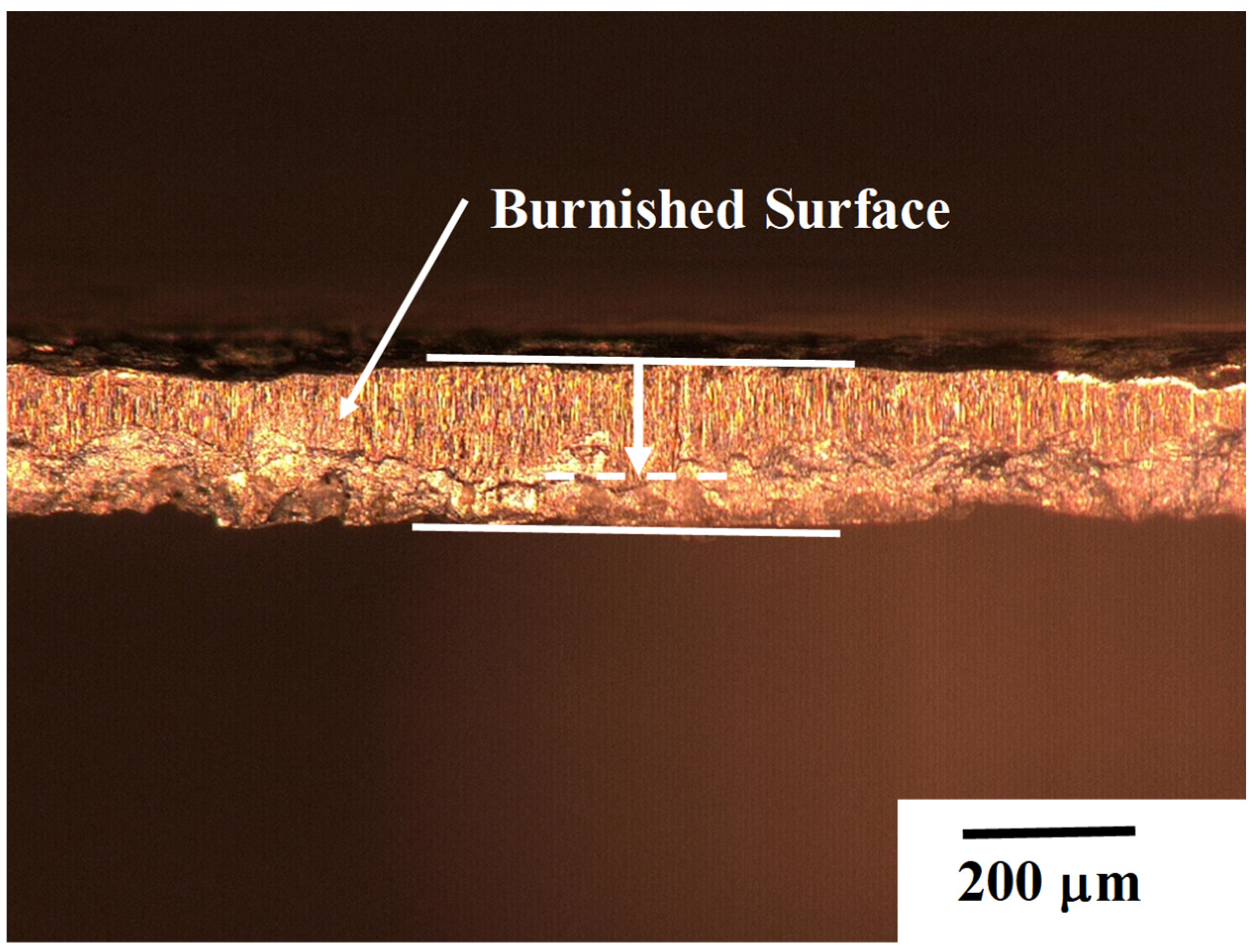
3.3. Selective Removal of Un-Nitrided Parts by Mechanical Blasting

Two nitrided AISI316L substrates were sandblasted for 600 s to remove the un-nitrided parts of substrates. Figure 8 depicts optical microscopy images for the blasted AISI316L substrates. The substrate with a negative micropattern on the T-shaped unit transforms into a punch with its T-shaped head, as shown in Figure 8a. On the other hand, the substrate with a positive micropattern on the T-shaped unit changes to a die with its T-shaped cavity, as depicted in Figure 8b. The as-blasted punch has sharp edges and corners on every X-Z and Y-Z plane in Figure 8a, while the as-blasted die also has steep edges and corners on each x-z and y-z plane in Figure 8b.
This mechanical blasting behavior proves that the nitrided parts have higher hardnesses than the silica particles’ hardness of 700 HV and that the borders of selectively nitrided regions in Figure 5a,b as well as Figure 6a,b change to be the edges of the punch head and die cavity in Figure 8a,b, respectively. The sharpness and steepness at the edges and corners of the punch and die can be much improved by slightly polishing the punch’s head and core-die surfaces, which will be discussed later.
A three-dimensional profilometer was utilized to precisely measure the punch head and die cavity widths and depths and to investigate the dimensional coordination between the piercing punch and die. Figure 9 depicts the punch head profile on the blasted substrate in Figure 8a. This punch head height is uniform and constant by H = 250 μm. The cross-sectional profile of the punch is measured along the line F–F’. The as-blasted punch head has a smooth surface with a maximum height variation of 5 μm and dull edge curvature of 15 μm. If it is slightly polished down to the line J–J’ by 15 μm, the head surface deviation is minimized down to 0.2 to 0.3 μm, and the punch edge’s width is sharpened down to 1 μm, which is sufficient to be used as a fine-piercing punch in practical applications.
Figure 10 shows the die profile together with the cross-sectional view along the line f–f’. The sharp and steep edges are also attained in this as-blasted die cavity. The maximum die cavity depth reaches 500 μm. Some deviations from average depth are observed from left to right on the cross-sectional profile due to manual operations in mechanical blasting. A homogeneous depth profile was attained as a die cavity. When slightly buffing the die top surface down to the line j–j’ by 10 to 15 μm, its surface roughness and the die edge’s curvature were improved to be less than 0.5 μm and 1 μm, respectively.
In Figure 9 and Figure 10, the side surfaces of T-shaped punch head and the wall surfaces of the T-shaped die cavity formed to be steep and straight enough in order to be used as a piercing punch and die without further mechanical polishing. By conducting measurements along the selected sections in Figure 9 and Figure 10, the dimensional clearance between the as-blasted punch and die is evaluated with reference to the electrical steel sheet’s thickness.
Table 1 summarizes the measured widths of the as-blasted punch head along the lines from A–A’ to H–H’ in Figure 9 as well as the as-blasted die cavity along the lines from a–a’ to h–h’ in Figure 10. Almost all widths of the T-shaped punch head are within the tolerance from +0.3% to −2% of the reference widths of the micropatterns on the screen. In particular, the thinner regions of T-shaped geometry have a shortage in width after mechanical blasting; e.g., the measured width along the E–E’ line is thinner by 2% from the original width in the tailored T-shaped geometry on the screen. All the measured widths of T-shaped cavity positively deviated from the reference data on the screen; e.g., the width along the e–e’ line is 1.039, which is 4% broader than the reference width of 1.0 mm on the screen. This positive deviation suggests that more a accurate dimension can be attained by redesigning the original micropattern for the T-shaped die by considering mechanical blasting allowances. Even in the present setup of the punch and core-die, the clearance between the two is automatically fixed in a positive form from +0.3% to +20% of the electrical steel sheet’s thickness.

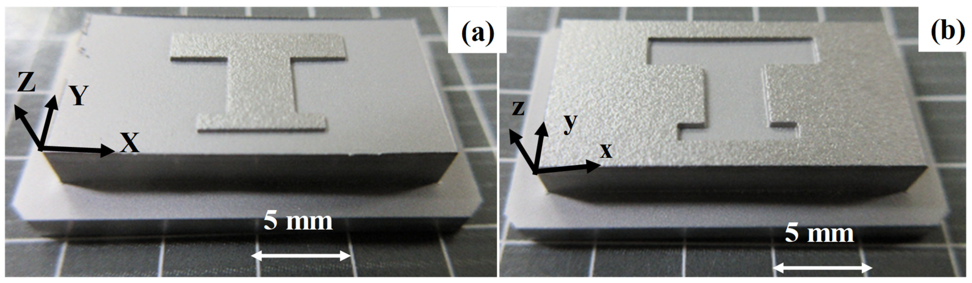
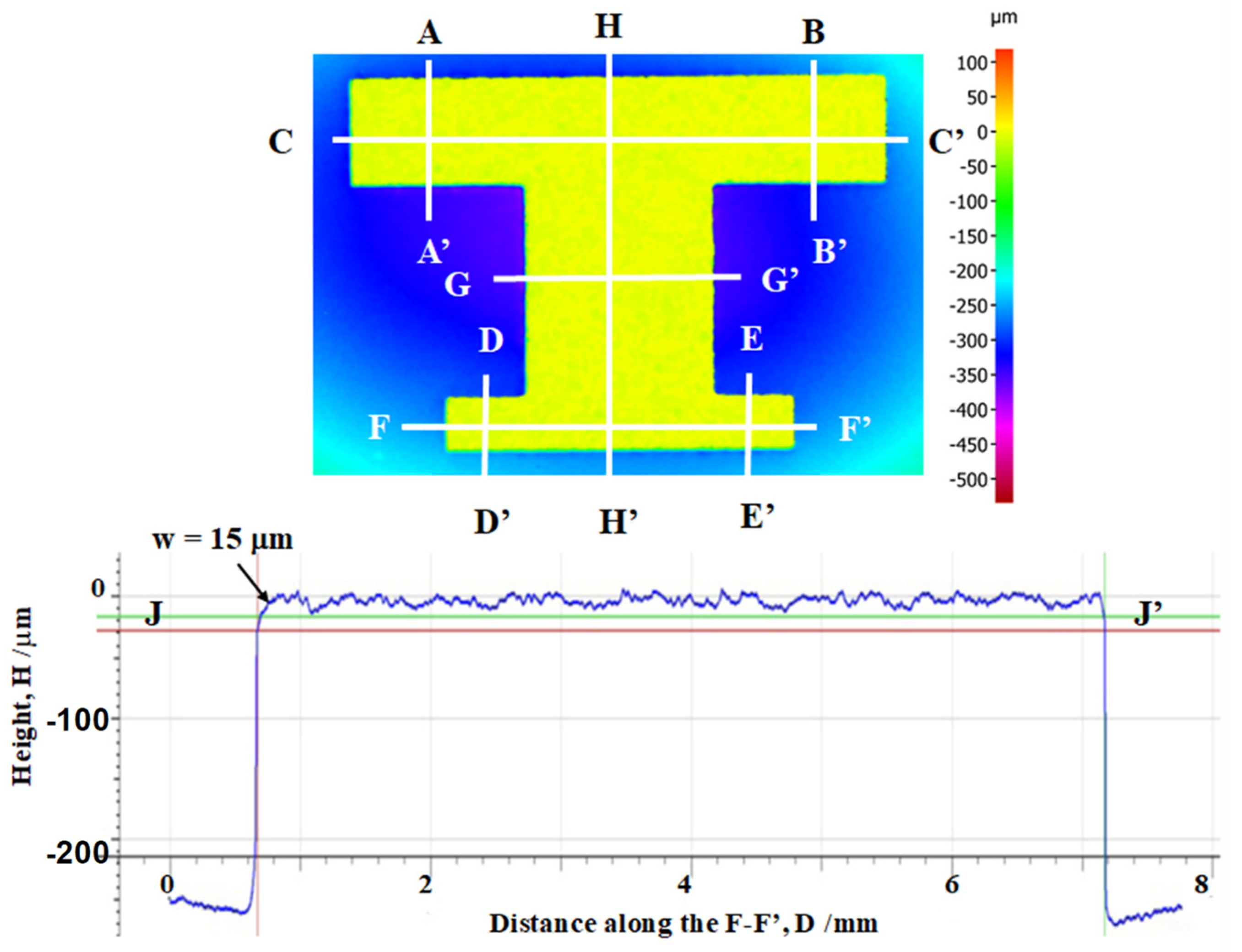
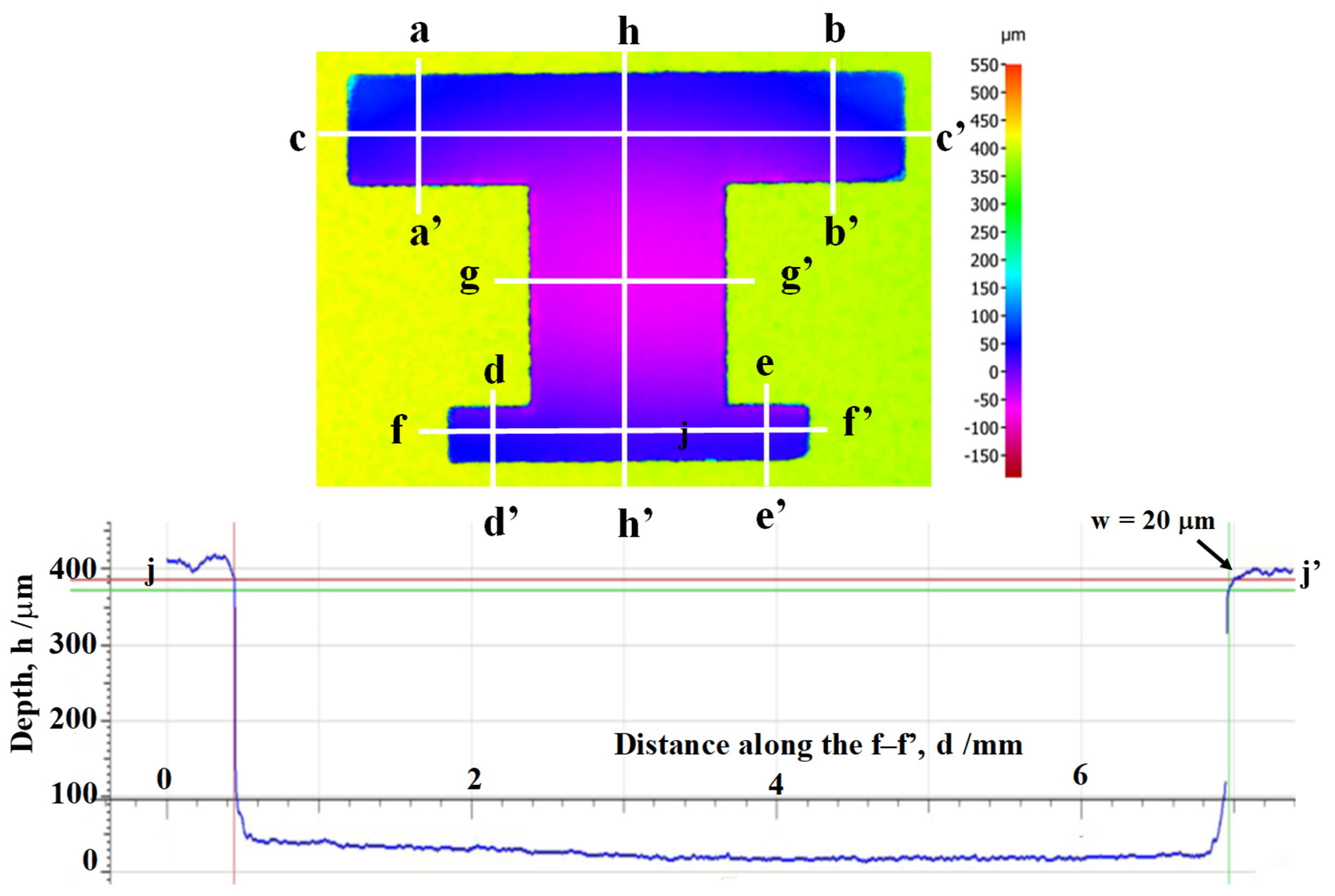
3.4. Fine Piercing of Electrical Steel Sheets

Electrical steel sheets with a thickness of 200 μm were used as a work material for the piercing experiment. After the adjustment of upper and lower die sets, a CNC stamping system was utilized under the loading schedule. Figure 11 shows the optical microscopy image on the pierced electrical steel part and the T-shaped skeleton of the work sheet, respectively. The T-shaped electrical steel core-unit is successfully punched out without significant distortions in dimension. Optical microscopy was utilized to describe the sheared hole surface in the skeleton. As shown in Figure 12, the burnished surface area ratio is 70% of the entire sheared surface without a significant deviation in fractured surface. As reported in [24], the plasma nitrided punch with the diameter of 2.00 mm was utilized in continuous piercing experiments; the average burnished surface area ratio reached 80% during piercing under nearly zero clearances. This suggests that a higher burnished surface area ratio can be obtained by implementing dimensional adjustments in the micropattern for the die at the initial CAD of the plasma-assisted 3D-printing procedure.

4. Discussion

In the standard manufacture of punches and dies for metal forming, they are shaped and finished by mechanical machining and milling. The finished punches and dies are case hardened and adjusted in geometry. In these methods, the number of cutting paths as well as the amount of CAM data exponentially increased with complexity and dimensional accuracy with respect to the geometry of the punch head and die cavity. Total tact time in those steps consisted of the preparation of CAM data for machining and milling; the actual cutting and finishing with positioning controls of tools; and heat treatment. In addition, this tact time is also enhanced exponentially by downsizing the products.
The present plasma-assisted 3D printing process is free from machining except for grinding and polishing processes used to adjust the edge sharpness and surface roughness of the punch and die. No CAM data or no cutting tools were used. The punch head and the die surfaces are hardened enough and can be directly utilized as special tools for metal forming without additional heat treatment and coating. Furthermore, this plasma-assisted 3D-printing processes for producing the special tools are not constrained by the complexity and dimensional accuracy of the product model.
Let us count the tact time for the three steps in the present approach. Screen-printing complex-shaped micro-patterns onto the substrate surface requires 300 s or 5 min for each substrate, including setting, adjusting, and polishing times. Plasma nitriding requires six hours per batch, including heating, nitriding processes, and cooling times. Sandblasting is performed within 800 s per substrate, including preliminary running, blasting, and adjustment times. Hence, the total tact time excluding the final polishing time reaches 23.8 ks in order to complete the plasma-assisted 3D-printing process. This tact time is invariant relative to the complexity and down-sizing process of the punch head and die cavity. This plasma-assisted 3D-printing process is suitable for die fabrication for the small-/medium-scaled production of parts, as well as the multi-piece production of miniature components [25,26]. Various micro-pattering processes are available as a solution to satisfy the demanded dimensional accuracy of products.
The nitrogen supersaturation process via low temperature plasma nitriding plays an essential role in transforming the CAD data of micropatterns to tailored special tools for applications. The inner nitriding behavior for die matrix materials has influence on plasma-assisted 3D-printing processes. The nitrogen supersaturation of stainless steels was featured by an improvement in their corrosion roughness [17,27] as well as the control of hardness by a higher averaged nitrogen solute content [10,28,29]. Higher corrosion and wear toughness are favored for continuous piercing operations in the air coupled with a minimum quantity of lubrication in any circumstance. In particular, the nitrided die surfaces are free from the adhesion of work debris particles during dry-cold stamping. Distinct from other plasma nitriding processes [30,31], no iron and chromium nitrides are precipitated in the nitrided AISI316 matrix, as reported in [32,33]. This nitrogen supersaturated die has no secondary phases to initiate fatigue cracking in the matrix; the die’s life is expected to be prolonged even in dry stamping operations [34].
The dimensional accuracy of punch and die made by mechanical machining and milling is determined by the cutting speed, the depth of cut, and the cutting path [35]. In the present plasma-assisted 3D-printing process, its accuracy is first governed by the resolution of the screen for micro-patterning; e.g., the tolerance for micro-patterning the screen film is ±15 μm. As listed in Table 1, the dimensional deviation of each width from A–A’ to H–H’ in the T-shaped punch head is almost within this tolerance. That is, the dimensional accuracy of T-shaped punch is mainly determined by the spatial resolution of screens. On the other hand, the entire measured section length from a–a’ to h–h’ positively deviated by +20 to +25 μm in Figure 10 in addition to the above tolerance. This is due to excess mechanical blasting at the border between the un-nitrided, T-shaped region and the nitrided surfaces. This over-blasting problem is solved by rationally adjusting CAD data for the positive screen to consider blasting allowances by a positive deviation of +20 to +25 μm during plasma-assisted 3D-printing. Then, the clearance between the plasma 3D-printed punch and die is automatically narrowed to be less than +5 to +10 μm or 2.5 to 5% of the electrical steel sheet’s thickness.
As stated in [8,36,37,38], the fine piercing behavior is sustained by the sharpness of the edge at the punch and die and the steepness of their side surfaces in addition to the clearance between the punch and the die. Figure 9 and Figure 10 show that the as-blasted edge width (w) of the punch is 15 μm and it is w = 20 μm at the edge of the die. The as-blasted punch and die are utilized in the present study; piercing performance was much improved by sharpening this edge. The edge’s width reduced down to 1 μm only by polishing and buffing the punch head and die surface by 10 to 15 μm. As shown in Figure 9 and Figure 10, the as-blasted punch head and die cavity have steep and straight side surfaces so that the tapered widths between the punch head and bottom and between the die cavity top and bottom are less than 1 μm.
The electrical steel sheets were finely pierced with success into T-shaped units only by using the as-blasted punch and die. This suggests that the present plasma-assisted 3D-printing process is expected to work as a die technology for the fabrication of miniature and complex-shaped parts and members. Currently, miniature motors in sizes from sub-millimeters to millimeters utilize a small-sized magnet instead of the iron core [39]. The plasma-assisted 3D-printed punch and die are suitable for the fabrication of miniature iron cores for millimeter-sized and sub-millimeter-sized motors instead of using permanent magnets. A lead frame in the packaging of semiconductor units is a typical thin and flat member with complex geometry that has been produced by chemical etching [40]. The dull edge of microtextures in the frame becomes an issue of deterioration in product quality. Fine piercing with the use of plasma 3D-printed punch and die provides a method to attain nearly full-burnished hole surfaces and can minimize the damaged zones in the product. Long tact times for chemical etching, polishing, and the post-treatments are reduced by this fine piercing process. A miniature connector is made from copper alloys with high strength and ductility; most dies suffered from short die life and low product quality [41]. Due to nitrogen supersaturation in this plasma-assisted 3D printing process, the punch and die have sufficient hardness and strength to prolong their tool lives even under when fine piercing high-strength copper alloy sheets.

5. Conclusions

Low temperature plasma nitriding processes were utilized to assist the 3D printing process to simultaneously fabricate finely pierced austenitic stainless steel AISI316L punch and die. There was no utilization of machining, milling processes, and heat treatment, and there was no use of CAM data in this tooling process, which significantly reduced the tact times for die-based metal formation. In addition, this method is free from the geometric complexities of the product model. Once the micro-patterns were printed onto the flat or curved die substrate surfaces, the punch and die with the tailored head and cavity to each metal formation are fabricated in the same procedure without additional treatments. Furthermore, the dimensional accuracy needed for special tooling is marginable by controlling spatial resolutions in micro-patterning. Micro-patterned AISI316L substrates with the use of CAD-oriented screen films straightforwardly transform to a punch-and-die pair with sufficient hardness and strength for piercing experiments. Negative micro-patterns relative to T-shaped motor-core unit change to a hardened punch with its T-shaped head, while its positive micro-pattern turns out to be a die with a T-shaped cavity. The clearance between the two is automatically determined by the dimensional tolerance in micro-patterning.
The burnished surface area ratio reaches 70% even when using the as-blasted punch and die. This proves that nearly the same accuracy is attained, as reported in the literature, where the circular punch and die were used for fine piercing under nearly zero clearance. With additional buffing and polishing steps for sharpening the edge of the punch and core-die, this piecing process for electrical steel sheets with a T-shaped motor-core unit was much improved with higher qualifications in its magnetic properties. In addition, the standard piercing die design for the production of motor cores is renewed from unit-by-unit stamping to single-shot processes in order to punch out the entire motor-core sheet product by single-shot stamping. In particular, in the production of miniature motor cores and connectors, the present plasma-assisted 3D-printing process provides an efficient method to fabricate punch and die arrays for multi-piece products from tailored micro-patterns for industrial applications.

Author Contributions

Conceptualization, T.A. and Y.S.; methodology, T.A.; software, T.A.; validation, Y.S., T.Y. and T.S.; formal analysis, T.Y.; investigation, T.A., Y.S. and T.S.; data curation, T.Y. and T.S.; writing—original draft preparation, T.A.; writing—review and editing, Y.S. and T.S.; supervision, T.S.; project administration, Y.S. All authors have read and agreed to the published version of the manuscript.

Funding

This research was financially supported in part by the METI-Program in the Supporting Industry project from 2019 to 2022.

Acknowledgments

The authors would like to express their gratitude to S. Kurozumi (Nano-Film Coat, LLC.) for his help in the stamping experiments.

Conflicts of Interest

The authors declare no conflict of interest.

References

  1. Schmidt, K. Manufacturing Processes for Engineering Materials, 5th ed.; Prentice Hall: Hoboken, NJ, USA, 2008. [Google Scholar]
  2. Avanish, D. Laser beam machining—A review. Int. J. Mach. Tools Manuf. 2008, 48, 609–628. [Google Scholar]
  3. Gaertner, E.; Polise, V.; Tagliaferri, F.; Palumno, B. Laser micro machining of alumina by a picosecond laser. J. Laser Micro/Nanoeng. 2018, 13, 76–84. [Google Scholar]
  4. Aizawa, T.; Inohara, T. Pico- and Femto-Second Laser Micromachining for Surface Texturing. In Micromachining; Stanimirovíc, Z., Stanimirovíc, I., Eds.; IntechOpen: London, UK, 2019; pp. 1–23. [Google Scholar]
  5. Zhang, J.; Jung, Y.G. (Eds.) Additive Manufacturing—Materials, Processes, Qualifications and Applications; Elsevier: Amsterdam, The Netherlands, 2018. [Google Scholar]
  6. Surface Finishing for Additive Manufacturing. Available online: https://isofinishing.com/additive-manufacturing/ (accessed on 4 April 2020).
  7. Gaffet, E.; Caër, G.L. Micro-milling. In NanoMaterials and NanoChemistry; Bréchignac, C., Houdy, P., Lahmani, M., Eds.; Springer: Berlin/Heidelberg, Germany, 2008. [Google Scholar]
  8. Tyagi, P.; Goulet, T.; Riso, C.; Stephenson, R.; Chuenprateep, N.; Schlitzer, J.; Benton, C.; Garcia-Moreno, F. Reducing the roughness of internal surface of an additive manufacturing produced 316 steel component by chempolishing and electropolishing. Addit. Manuf. 2019, 25, 32–38. [Google Scholar] [CrossRef] [Green Version]
  9. Chen, N.; Ma, G.; Zhu, W.; Godfrey, A.; Shen, Z.; Wu, G.; Huang, X. Enhancement of an additive-manufactured austenitic stainless steel by post-manufacture heat-treatment. Mater. Sci. Eng. A 2019, 759, 65–69. [Google Scholar] [CrossRef]
  10. Katoh, T.; Aizawa, T.; Yamaguchi, T. Plasma assisted nitriding for micro-texturing onto martensitic stainless steels. Manuf. Rev. 2015, 2, 1–7. [Google Scholar] [CrossRef] [Green Version]
  11. Shiratori, T.; Aizawa, T.; Saito, Y.; Wasa, K. Plasma printing of an AISI316 micro-meshing punch array for micro-embossing onto copper plates. J. Met. 2019, 9, 396. [Google Scholar] [CrossRef] [Green Version]
  12. Aizawa, T.; Saito, Y.; Hasegawa, H.; Wasa, K. Fabrication of optimally micro-textured copper substrates by plasma printing for plastic mold packaging. Int. J. Autom. Technol. 2020, 14, 200–207. [Google Scholar] [CrossRef]
  13. Aizawa, T.; Shiratori, T.; Komatsu, T. Micro-/nano-structuring in stainless steels by metal forming and materials processing. In Electron Crystallography; IntechOpen: London, UK, 2020; Chapter 5; pp. 101–122. [Google Scholar]
  14. Aizawa, T. Low temperature plasma nitriding of austenitic stainless steels. In Stainless Steels and Alloys; IntechOpen: London, UK, 2018; Chapter 3; pp. 31–50. [Google Scholar]
  15. Borgioli, F.; Galvanetto, E.; Bacci, T. Low temperature nitriding of AISI300 and 200 series austenitic stainless steels. Vacuum 2016, 127, 51–60. [Google Scholar] [CrossRef]
  16. Farghali, A.; Aizawa, T.; Yoshino, T. Microstructure/mechanical characterization of plasma nitrided fine-grain austenitic stainless steels in low temperature. J. Nitrogen 2021, 2, 244–258. [Google Scholar] [CrossRef]
  17. Borgioli, F.; Galvanetto, E.; Bacci, T. Corrosion behavior of low temperature nitrided nickel-free, AISi200 and AISI300 series austenitic stainless steels in NaCl solution. Corros. Sci. 2018, 136, 352–365. [Google Scholar] [CrossRef]
  18. Aizawa, T.; Yoshihara, S.-I. Microtexturing into AISI420 dies for fine piercing of micropatterns into metallic sheets. J. JSTP 2019, 60, 53–57. [Google Scholar] [CrossRef]
  19. Marcos, G.; Guilet, S.; Clymand, F.; Thiriet, T.; Czerwuec, T. Stainless steel patterning by combination of micro-patterning and driven strain produced by plasma assisted nitriding. Surf. Coat. Technol. 2011, 205, 5275–5279. [Google Scholar] [CrossRef]
  20. Kurosaki, Y.; Mogi, H.; Fujii, H.; Kubota, T.; Shiozaki, M. Importance of punching and workability in non-oriented electrical steel sheets. J. Magn. Magn. Mater. 2008, 320, 2474–2480. [Google Scholar] [CrossRef]
  21. Aizawa, T.; Rsasi, I.; Yunata, E.E. High density RF-DC plasma nitriding under optimized conditions by plasma-diagnosis. J. Appl. Sci. 2022, 12, 3706. [Google Scholar] [CrossRef]
  22. Farghali, A.; Aizawa, T. Nitrogen supersaturation process in the AISI420 martensitic stainless steels by low temperature plasma nitriding. ISIJ Int. 2018, 58, 401–407. [Google Scholar] [CrossRef] [Green Version]
  23. Aizawa, T.; Shiratori, T.; Komatsu, T. Integrated manufacturing of fine-grained stainless steels for industries and medicals. In Engineering Steels and High Entropy-Alloys; IntechOpen: London, UK, 2020; Chapter 1; pp. 3–26. [Google Scholar]
  24. Katsuta, E.; Aizawa, T.; Morita, H.; Dohda, K.; Anzai, M. Fine piercing of electromagnetic steel sheets by micro-punches under nearly zero clearance. Procedia Manuf. 2018, 15, 1459–1466. [Google Scholar] [CrossRef]
  25. Susman, G.; Warren, A.; Ding, M. Product and Service Innovation in Small and Medium-Sized Enterprises; NIST-REP 05-480-5834; 2006. Available online: https://www.smeal.psu.edu/fcfe/research/white/nist06.pdf (accessed on 4 April 2020).
  26. Pratap, A.; Patra, K.; Dyakonov, A.A. Manufacturing miniature products by micro-grinding: A review. Procedia Eng. 2016, 150, 969–974. [Google Scholar] [CrossRef] [Green Version]
  27. Aizawa, T.; Wasa, K. Plasma printing of micro-nozzles with complex shaped outlets into stainless steel sheets. J. Micro-Nano-Manuf. 2019, 7, 034502. [Google Scholar] [CrossRef]
  28. Bell, T. Surface engineering of austenitic stainless steels. Surface Eng. 2002, 18, 415–422. [Google Scholar] [CrossRef]
  29. Wang, L.; Ji, S.; Sun, J. Effect of nitriding time on the nitrided layer of AISI304 austenitic stainless steel. Surf. Coat. Technol. 2006, 200, 5067–5070. [Google Scholar] [CrossRef]
  30. Kuwahara, H. Surface Modification of Iron Alloys by Plasma Nitriding and Carburizing. Ph.D. Thesis, Kyoto University, Kyoto, Japan, 1992. [Google Scholar]
  31. Hiraoka, Y.; Inoue, K. Prediction of nitrogen distribution in steels after plasma nitriding. Denki-Seiko 2010, 86, 15–24. [Google Scholar]
  32. Lu, S.; Zhao, X.; Wang, S.; Li, J.; Wei, W.; Hu, J. Enhancement by plasma nitriding at low gas pressure for 304 austenitic stainless steel. Vacuum 2018, 145, 334–339. [Google Scholar] [CrossRef]
  33. Dong, H. S-phase surface engineering of Fe-Cr, Co-Cr and Ni-Cr alloys. Int. Mater. Rev. 2011, 55, 65–98. [Google Scholar] [CrossRef]
  34. Murata, I.; Sakamoto, M. Properties of High Nitrogen Steels. Agune 2005, 166–168. [Google Scholar]
  35. Karino, K. Machining and Milling of Die Materials; Nikkan-Kogyo-Shinbun: Tokyo, Japan, 2011. [Google Scholar]
  36. Aizawa, T.; Morita, H. Dry progressive stamping of copper-alloy snaps by the plasma nitrided punches. Mater. Sci. Forum 2018, 920, 28–33. [Google Scholar] [CrossRef]
  37. McCarthy, C.T.; Hussey, M.; Gilchrist, M.D. On the sharpness of straight edge blades in cutting soft solids; Part I—Indentation experiments. Eng. Fract. Mech. 2007, 74, 2205–2224. [Google Scholar] [CrossRef]
  38. Shiratori, T.; Yoshino, T.; Suzuki, Y.; Aizawa, T. Deformation and transformation characteristics in micropunching of stainless steel AISI304. In Proceedings of the 3rd WCMNM, Raleigh, NC, USA, 10 September 2019; pp. 130–133. [Google Scholar]
  39. Miniature Motors. Available online: https://rdc.portescap.com/products (accessed on 4 April 2020).
  40. Production Line of Lead Frames. Available online: https://www.mitsui-high-tec.com/ja/products/lf/feature.php (accessed on 4 April 2020).
  41. Miniature Copper-Alloy Connectors. Available online: http://www.farnell.com/datasheets/1072747.pdf (accessed on 4 April 2020).
Figure 1. Plasma assisted 3D-printing procedure to fabricate the complex-shaped punch and die without use of mechanical machining and milling. (a) Initial AISI316L substrate, (b) micropatterning onto substrate surfaces, (c) plasma nitriding through unprinted surfaces, and (d) blasting to remove un-nitrided parts.
Jmmp 06 00049 g001
Figure 2. A schematic view and photo of plasma 3D-printing facilities used in the present experimental setup. (a) Screen-printing for micropatterning onto the substrate, (b) plasma nitriding for selective nitrogen supersaturation relative to unprinted surface areas, and (c) sand-blasting for selective removal of un-nitrided parts.
Jmmp 06 00049 g002
Figure 3. Schematic view and photo of the experimental setup with the use of CNC stamping system for piercing electrical steel sheets with a thickness of 0.2 mm with the use of plasma-printed punch and die.
Jmmp 06 00049 g003
Figure 4. Screen printing of micropatterns onto the AISI316L substrate surface. (a) Printing the negative pattern to T-shaped motor-core sheet unit onto the die surface, and (b) printing its positive pattern onto the die surface.
Jmmp 06 00049 g004
Figure 5. Optical microscopy images on nitrided substrates with negative and positive micropatterns. (a) Substrate with the negative micropattern, and (b) substrate with the positive micropattern.
Jmmp 06 00049 g005
Figure 6. SEM-EDX analyses on the selectively nitrided substrate surface. (a) SEM image and element mapping of Ti and Cr at the A-region in Figure 5a and (b) SEM image and element mapping of Ti and Cr at the B-region in Figure 5b.
Jmmp 06 00049 g006
Figure 7. SEM-EDX analyses on the cross-section of T-shaped substrate in Figure 5b. (a) The cross-section of T-shaped AISI316L substrate, (b) SEM image on the cross-section across the border between the unprinted and printed zones, and (c) element mapping of N, Cr, Ti, and Si on the cross-section.
Jmmp 06 00049 g007
Figure 8. Optical microscopy image on the AISI316L substrates after sand-blasting for 600 s. (a) A nitrided AISI316L punch with its T-shaped head, and (b) a nitrided AISI316L core-die with its T-shaped cavity.
Jmmp 06 00049 g008
Figure 9. Three-dimensional profile of T-shaped punch head with its cross-sectional view along the line F–F’.
Jmmp 06 00049 g009
Figure 10. Three-dimensional profile of T-shaped die cavity with its cross-sectional view along the line f–f’.
Jmmp 06 00049 g010
Figure 11. Optical image on the pierced electrical steel sheet and T-shaped skeleton.
Jmmp 06 00049 g011
Figure 12. Optical microscopy image on the sheared surface of electrical steel sheet by the present piercing experiment with the use of as-blasted punch and die.
Jmmp 06 00049 g012
Table 1. The measured widths of T-shaped punch head and die cavity in Figure 9 and Figure 10 with reference to the CAD data of screen films.
.A-A’
a-a’
B-B’
b-b’
C-C’
c-c’
D-D’
d-d’
E-E’
e-e’
F-F’
f-f’
G-G’
g-g’
H-H’
h-h’
Screen (mm)2.02.010.01.01.06.53.57.0
T-shaped punch (mm)2.0011.99110.0010.9780.9716.5123.4766.990
T-shaped die (mm)2.0232.03910.0451.0471.0396.5313.5617.073
Clearance (mm)0.0110.0240.0220.0340.0350.00950.0430.0415
Publisher’s Note: MDPI stays neutral with regard to jurisdictional claims in published maps and institutional affiliations.

