Abstract
Low-cost infrared (IR) thermal cameras are powering a rising market of industrial and consumer applications. Complementary metal-oxide-semiconductor (CMOS)-based thermopile arrays are proven thermal imagers that can be monolithically integrated into low-cost and low-power-consumption formats for high-volume manufacturability. Here we present a simple method to evaluate the cross-talk of these arrays and propose a numerical model for device optimization.
1. Introduction
Room temperature IR thermal imaging is increasingly important for a variety of applications, including smart homes, healthcare, security, and automotive [1]. In addition, with the emerging trend of miniaturization of optical systems on-chip, numerous possibilities exist within the broader application market, including thermal cameras integrated into smartphones, watches, or wearables [2]. When deployed for such applications, or within the internet of things (IoT) environment, IR cameras need to be low in cost (so they can be deployed in large numbers), and have low-power consumption (so they can be battery or energy-harvesting operated) [3]. Among various current technologies [1,2], CMOS-based thermopile IR cameras stand out in terms of manufacturing flexibility and offer cost and power consumption compatible with the consumer electronics and IoT requirements [3]. Here we present a novel approach for cross-talk measurement of a thermopile detector array. The measurement approach does not require a light source, or an on-chip heater [1], thus significantly simplifying the analysis. A numerical model, in agreement with the experimental observations, is also proposed, and used to demonstrate design optimization.
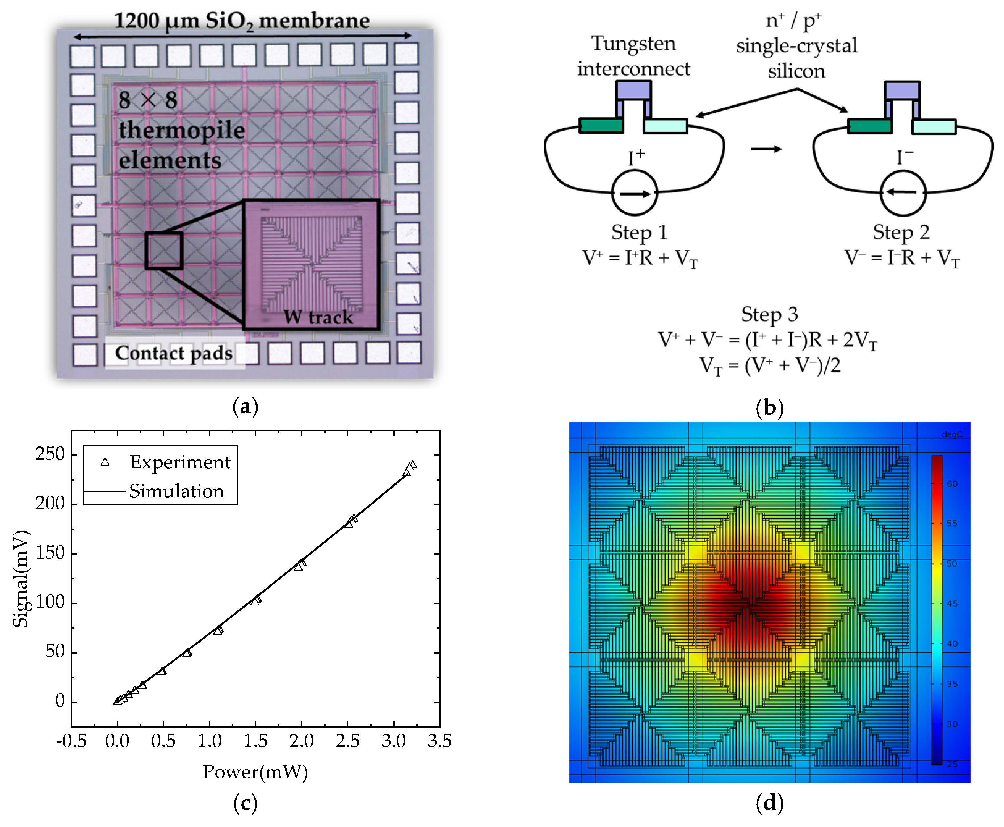
2. Fabrication and Results
Our device was fabricated using a commercial CMOS process, followed by back deep reactive ion etching (DRIE) to form the membrane. Highly doped single-crystal Si layers formed the p+ and n+ thermopile elements, while tungsten (W) interconnect layers formed heatsinking tracks between the pixels, as well as interconnects between the Si p+ and n+ elements. The membrane was 1200 × 1200 µm and ~5 µm thick (Figure 1a). A device having an array size of 8 × 8 elements was fabricated as a proof-of-concept. The individual thermopile array elements consisted of 52 thermocouples arranged on a single pixel (Figure 1a inset).
Figure 1.
(a) Optical image of the thermopile array. The chip size is 1.76 × 1.76 mm; (b) Schematic diagram showing the bidirectional electrical biasing measurement method; (c) Experimental data showing the thermoelectric voltage generated by the heated pixel, at powers from 0 to 3.5 mW, and results from the numerical model; (d) Simulated temperature distribution from a central heated pixel to neighboring pixels.
To measure the cross-talk, we used a bidirectional electrical biasing approach to obtain the thermoelectric voltage generated by a thermopile (pixel) under thermal stress. A range of biasing currents (~10 to 200 μA in our case) was applied to a pixel in both negative and positive directions, which as a result experienced ohmic heating. The thermoelectric voltage was then calculated by simply averaging the bidirectional generated voltages. The cross-talk was finally evaluated by comparing the voltage generated by an adjacent pixel to that of the heated pixel (Figure 1b). Compared to traditional methods based on light sources and complex focusing optics, our method is significantly easier to apply. In addition, it uses only the heat generated internally by the pixel, and thus does not suffer from light leakage to adjacent pixels, which can be challenging to control and quantify.
Author Contributions
All authors contributed equally. All authors have read and agreed to the published version of the manuscript.
Funding
EPSRC Grant No. EP/S031847/1.
Conflicts of Interest
The authors declare no conflict of interest.
References
- Kruse, P.W. Uncooled Thermal Imaging Arrays, Systems, and Applications; SPIE: Bellingham, WA, USA, 2011. [Google Scholar]
- Popa, D.; Udrea, F. Towards Integrated Mid-Infrared Gas Sensors. Sensors 2019, 19, 2076. [Google Scholar] [CrossRef] [PubMed]
- Popa, D.; Ali, S.Z.; Hopper, R.; Dai, Y.; Udrea, F. Smart CMOS mid-infrared sensor array. Opt. Lett. 2019, 44, 4111. [Google Scholar] [CrossRef] [PubMed]
Publisher’s Note: MDPI stays neutral with regard to jurisdictional claims in published maps and institutional affiliations. |
© 2020 by the authors. Licensee MDPI, Basel, Switzerland. This article is an open access article distributed under the terms and conditions of the Creative Commons Attribution (CC BY) license (https://creativecommons.org/licenses/by/4.0/).