Proceeding Paper

Fabrication of Structured Boron-Doped Diamond Films for Electrochemical Applications †

1
Institute of Physics, Czech Academy of Sciences, Cukrovarnická 10, 16200 Prague 6, Czech Republic
2
UNESCO Laboratory of Environmental Electrochemistry, Department of Analytical Chemistry, Faculty of Science, Charles University, Albertov 6, 12843 Prague 2, Czech Republic
*
Author to whom correspondence should be addressed.
Presented at the Eurosensors 2018 Conference, Graz, Austria, 9–12 September 2018.
Proceedings 2018, 2(13), 984; https://doi.org/10.3390/proceedings2130984
Published: 29 November 2018
(This article belongs to the Proceedings of EUROSENSORS 2018)

Abstract

:
In the present study, we introduce various technological approaches for fabrication of structured boron-doped diamond (BDD) electrodes, i.e., nanocones and nanorods which are used as working electrodes for electrochemical measurements. Structured BDD were realized either by reactive ion etching employing gold nanoclusters as the mask or by thermo-catalytically induced modification of the diamond surface. All samples were characterized in terms of surface morphology (scanning electron microscopy images), chemical composition (Raman spectroscopy) and electrochemical properties (anodic stripping voltammetry).

1. Introduction

In recent years, research has been focused on developing electrochemical sensors for heavy metals analysis at very low molar concentrations. Electrochemical sensors are promising devices due to low detection limits, high sensitivity, high surface area, good reproducibility, better signal-to-noise ratio, and selective sensing in a mixture of metal ions [1]. In general, the chemical information originated by the physical property of the system or by the reaction of the species present in the analyte is utilized in the receptor unit (working electrode), which is further transformed in electrical signal by the potentiostat/galvanostat based electrochemical workstation as the transducer system. The results can be achieved by applying various modes of signal amplification techniques such as potentiometry, voltammetry, conductometry and electrochemical impedance spectroscopy. Moreover, various modifications of working electrode can be carried out to enhance the sensitivity, selectivity and reproducibility of the electrochemical sensor [2].
Boron-doped diamond (BDD) electrodes have attracted a considerable attention in electroanalytical detection of different analytes (including trace metals [3,4]) due to their extremely high chemical stability, a wide potential window in aqueous media with a low background current and stable surface state without the tendency to fouling. It has been shown that the BDD electrode exhibits properties like the mercury one: low detection limit (mid to low ppb range) for lead, cadmium, copper and silver with a reproducibility higher than 95% [5]. Moreover, it was observed that BDD had a higher (3–5 times higher) sensitivity to determine Pb2+and Cd2+ in comparison to glassy carbon electrodes [6], and also the Pb at sub-ppb levels in tap water is detectable by BDD electrodes [7]. Thus, the BDD electrode, particularly used in combination with anodic stripping voltammetry, appears as a suitable mercury-free tool for the detection of trace metals.

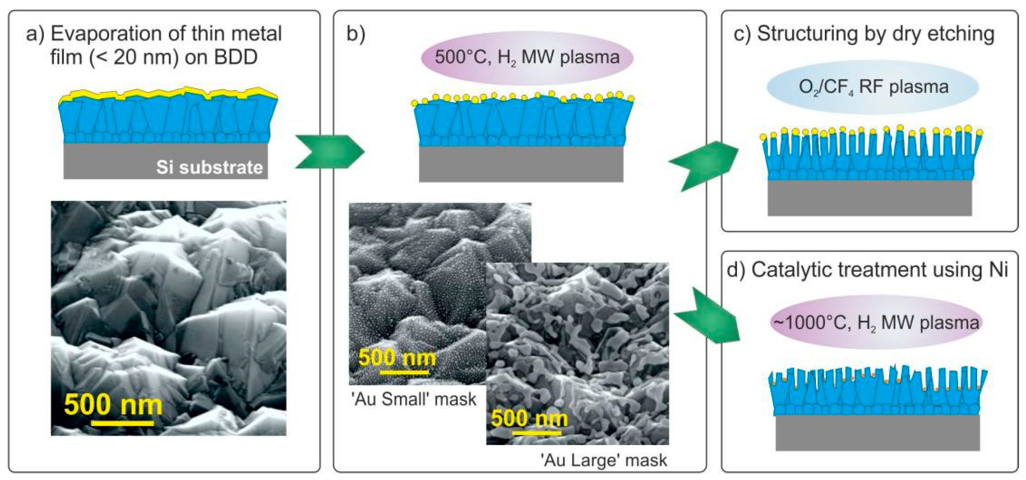
2. Materials and Methods

The BDD films (~2 μm in thickness) were grown using hot filament chemical vapor deposition on Si substrates by addition of trimethylboron (10,000 ppm) to the H2/CH4 gas mixture. The surface morphology of as-grown diamond films reveals crystals with diameter of 600–900 nm. The surface of diamond film was further structured either by reactive ion etching (RIE) in oxygen based gas mixture (O2 or CF4/O2) employing the gold nanoclusters as the masking material (Figure 1a–c) [8] or by thermo-catalytically driven reactions of nickel nanoclusters with the diamond surface (Figure 1a,b,d). In the first case, the gold nanoparticle’s masks were prepared by evaporating a thin Au layer (thickness 3 nm and 12 nm) which were further annealed to form ‘Au small’ or ‘Au large’ masks, respectively (Figure 1b). In the case of the catalytic modification, a thin Ni film (~10 nm) was evaporated and thermally treated (Figure 1b) and subsequently used for the catalytic etching at elevated temperature in hydrogen-rich microwave plasma (Figure 1d). To note, the thermal treatment of the thin metal layers was also realized in microwave plasma (H2, 500 °C for 10 min, Figure 1b). This treatment resulted in the formation of nano-sized metal droplets on diamond surface [9]. In the case of thermo-catalytically driven reactions, the processing of samples with Ni droplets were performed in the same microwave plasma system using different process parameters (H2, ~1000 °C for 30 min to 2 h, Figure 1d). The surface of samples was characterized by scanning electron microscopy (SEM, Maia3, Tescan Brno s.r.o, Czech Republic), the chemical composition was studied Raman spectroscopy (In via Renishaw Raman spectrometer with excitation wavelength 442 nm).

3. Results and Discussion

Figure 2 shows representative SEM images of selected samples with various surface morphologies depending on the fabrication process. In the RIE process the gas composition has a crucial effect on the final diamond film morphology (Figure 2a–d). If only oxygen RIE plasma is used without any masking material, the formed surface morphology is characterized by needle-like structures or so-called whiskers (see Figure 2a). Such whiskers are preferentially formed along grain boundaries because of differences in the chemical composition of grains (mainly sp3 carbon bonds) and grain boundaries (mainly sp2 bonds) in diamond film. Moreover, they can be formed also within the grains around intrinsic defects in the diamond crystals or in specific grains depending on their orientation [10]. The formation of whiskers can be suppressed by adding CF4 gas to the reactant mixture. Even an addition of a small amount of CF4 gas resulted in flatter surface, as it was observed in the case of intrinsic microcrystalline diamond (MCD) film [11]. In the case of boron-doped diamond film, in contrast to MCD film, the surface consists of small nanocone array (see Figure 2b) due to presence of a large amount of defects induced by boron incorporation into the diamond lattice.
When a mask of metal nanoclusters is applied during the RIE process, another surface morphologies can be achieved. For example, the surface can consist of both thick nanorods as well as whiskers after RIE in O2− plasma (Figure 2c). On the other hand, the surface will be dominated by thick nanorods (Figure 2d) when CF4/O2 plasma is applied.
In the case of catalytically driven reactions, first, the Ni film (with initial thickness of ~10 nm) is transformed into clusters in diameter of 80–100 nm, and then Ni catalytically transforms the diamond surface into graphitic form which is etched away in hydrogen rich plasma. It was observed, that at certain process conditions (at higher process temperature >900 °C), Ni clusters were incorporated into the diamond films. To note, Ni thin layer can be used also for transformation of diamond film to graphene at modified process condition [12]. However, Raman measurements did not confirm any changes in the chemical composition of the remaining diamond films.
The electrochemical properties of structured BDD electrodes were studied using standard ferrocyanide solution and their detection properties were tested against heavy metal ions (Cd2+, Pb2+). Regarding to electrochemical studies using ferrocyanide solution, all structured BDD films revealed an enlargement of the electrochemical potential window (from 3.5 V to ~3.8 V for as-grown and structured electrodes, respectively). Contrary to this observation, the peak separation of [Fe(CN)6]4−/3− increased in some cases up to 900 mV compared to 81 mV for the reference non-structured BDD electrode. Nevertheless, after the electrode surface activation (−3 V for 5 min in 2 M HNO3) all electrodes (i.e., structured and not-structured) revealed very similar electrochemical properties (i.e., comparable potential windows and peak separations). It was found out that the optimal electrode for heavy metal detection is the BDD electrode structured using an ‘Au small’ mask (etched in RIE by O2 or CF4/O2 plasma) due to the lowest relative standard deviation (RSD) estimated from 14 measurements in particular solution used for separate or simultaneous detection of Cd2+ and Pb2+.

4. Conclusions

We studied various technological approaches for fabrication of structured boron-doped diamond electrodes. The morphology can be tailored from densely arrayed whiskers to nanorods with or without needle-like structure. Different morphologies were fabricated either by reactive ion etching using gold nanoclusters as the mask or by thermo-catalytically induced modification of the BDD layer. The structured BDD electrodes showed great potential for electrochemical applications as confirmed by anodic stripping voltammetry measurements.

Author Contributions

A.K. and V.V. conceived and designed the experiments; O.S. and P.Š. performed the experiments; T.I. and Š.P. analyzed the data and wrote the paper.

Acknowledgments

This work was financially supported by EU project “Physics at your service” Nr. CZ.07.1.02/0.0/0.0/16_023/0000115.

Conflicts of Interest

The authors declare no conflict of interest.

References

  1. Sahoo, P.K.; Panigrahy, B.; Sahoo, S.; Satpati, A.K.; Li, D.; Bahadur, D. In situ synthesis and properties of reduced graphene oxide/Bi nanocomposites: As an electroactive material for analysis of heavy metals. Biosens. Bioelectron. 2013, 43, 293–296. [Google Scholar] [CrossRef] [PubMed]
  2. Pandey, S.K.; Singh, P.; Singh, J.; Sachan, S.; Srivastava, S.; Singh, S.K. Nanocarbon-based Electrochemical Detection of Heavy Metals. Electroanalysis 2016, 28, 2472–2488. [Google Scholar] [CrossRef]
  3. Le, T.S.; Da Costa, P.; Huguet, P.; Sistat, P.; Pichot, F.; Silva, F.; Renaud, L.; Cretin, M. Upstream microelectrodialysis for heavy metals detection on boron doped diamond. J. Electroanal. Chem. 2012, 670, 50–55. [Google Scholar] [CrossRef]
  4. Prado, C.; Wilkins, S.J.; Marken, F.; Compton, R.G. Simultaneous Electrochemical Detection and Determination of Lead and Copper at Boron-Doped Diamond Film Electrodes. Electroanalysis 2002, 14, 262–272. [Google Scholar] [CrossRef]
  5. McGaw, E.A.; Swain, G.M. A comparison of boron-doped diamond thin-film and Hg-coated glassy carbon electrodes for anodic stripping voltammetric determination of heavy metal ions in aqueous media. Anal. Chim. Acta 2006, 575, 180–189. [Google Scholar] [CrossRef] [PubMed]
  6. El Tall, O.; Jaffrezic-Renault, N.; Sigaud, M.; Vittori, O. Anodic Stripping Voltammetry of Heavy Metals at Nanocrystalline Boron-Doped Diamond Electrode. Electroanalysis 2007, 19, 1152–1159. [Google Scholar] [CrossRef]
  7. Dragoe, D.; Spătaru, N.; Kawasaki, R.; Manivannan, A.; Spătaru, T.; Tryk, D.A.; Fujishima, A. Detection of trace levels of Pb2+ in tap water at boron-doped diamond electrodes with anodic stripping voltammetry. Electrochim. Acta 2006, 51, 2437–2441. [Google Scholar] [CrossRef]
  8. Ižák, T.; Domonkos, M.; Babchenko, O.; Varga, M.; Rezek, B.; Jurka, V.; Hruška, K.; Kromka, A. Technological Aspects in Fabrication of Micro- and Nano-Sized Carbon Based Features: Nanorods, Periodical Arrays and Self-Standing Membranes. J. Electr. Eng. 2015, 66, 282–286. [Google Scholar] [CrossRef]
  9. Babchenko, O.; Kromka, A.; Hruska, K.; Michalka, M.; Potmesil, J.; Vanecek, M. Nanostructuring of diamond films using self-assembled nanoparticles. Open Phys. 2009, 7, 310–314. [Google Scholar] [CrossRef]
  10. Uetsuka, H.; Yamada, T.; Shikata, S. ICP etching of polycrystalline diamonds: Fabrication of diamond nano-tips for AFM cantilevers. Diam. Relat. Mater. 2008, 17, 728–731. [Google Scholar] [CrossRef]
  11. Izak, T.; Kromka, A.; Babchenko, O.; Ledinsky, M.; Hruska, K.; Verveniotis, E. Comparative study on dry etching of polycrystalline diamond thin films. Vacuum 2012, 86, 799–802. [Google Scholar] [CrossRef]
  12. Romanyuk, O.; Varga, M.; Tulic, S.; Izak, T.; Jiricek, P.; Kromka, A.; Skakalova, V.; Rezek, B. Study of Ni-Catalyzed Graphitization Process of Diamond by in Situ X-ray Photoelectron Spectroscopy. J. Phys. Chem. C 2018, 122, 6629–6636. [Google Scholar] [CrossRef] [PubMed]
Figure 1. Schematic drawing of fabrication process of structured boron-doped diamond films and corresponding surface morphology of as-grown BDD film and BDD films with two types of gold nanocluster’s masks (i.e., tilted-angle SEM images of BDD films with gold masks labelled as ‘Au small’ and ‘Au large’ with initial thickness of evaporated Au of 3 nm and 12 nm, respectively, after annealing). The fabrication process includes: (a) evaporation of thin metal film, (b) annealing (in hydrogen-plasma) to form metal clusters, and (c) reactive ion etching using O2/CF4 gas mixture or (d) catalytic thermal treatment using microwave plasma in hydrogen atmosphere.
Proceedings 02 00984 g001
Figure 2. Representative 45° angled-view SEM images of selected samples: (a) needle-like structures (whiskers), (b) BDD nanocones, (c) nanorods with needles or (d) without needles, and (e) top-view SEM images of nanoholes in diamond film obtained by catalytically etching using nickel nanoclusters and plasma treatment in hydrogen-rich microwave plasma.
Proceedings 02 00984 g002
Publisher’s Note: MDPI stays neutral with regard to jurisdictional claims in published maps and institutional affiliations.

