Abstract
This paper presents an ultra-low power, silicon-integrated readout for resonant MEMS strain sensors. The analogue readout implements a negative-resistance amplifier based on first-generation current conveyors (CCI) that, thanks to the reduced number of active elements, targets both low-power and low-noise. A prototype of the circuit was implemented in a 0.18-µm technology occupying less than 0.4 mm2 and consuming only 9 µA from the 1.8-V power supply. The prototype was earliest tested by connecting it to a resonant MEMS strain resonator.
1. Introduction
Low-power operation of strain sensors is particularly attractive in battery-supplied applications where it is not feasible to directly connect the sensor to the main supply. Strain gauge is the gold standard for strain sensing but it suffers from a power/resolution trade-off that prevents using it in battery-supplied applications. Resonant micro electro mechanical systems (MEMS), whose resonance frequency shifts with the applied strain, are promising because of their theoretically zero static power. Among them, the double-ended tuning fork (DETF) is a good candidate as a strain sensor since it resonates at a frequency f0 which is defined by the geometrical and physical properties, by the electrical bias, and by the applied strain [1]. Figure 1a outlines a possible layout for a DETF strain sensor, while Figure 1b shows its standard electro-mechanical model. The resolution of the DETF strain sensor, i.e., the minimum strain variation that gives rise to a fairly detectable frequency shift, is mainly set by the quality factor Q of the DETF resonator, which in turn depends on the mechanical properties (e.g., viscosity and mechanical friction) of the material interposed between the electrodes. Vacuum-packaged DETF allows low-power operation together with low noise and high resolution thanks to the very high Q factor, although the manufacturing of the MEMS is quite complex. Figure 1c shows the simulated admittance spectra of a vacuum-packaged DETF under different values of applied strain. The figure shows very narrow resonant spikes that prove the high-valued Q factor, and clearly demonstrates the ability of the DETF to sense the applied strain.
Figure 1.
(a) Standard layout for a DETF. (b) Equivalent electro-mechanical model of DETF with parasitic elements. (c) Typical admittance spectra of DETF without applied strain (red line) and with positive (yellow) or negative (blue) applied strain.
In any case, the DETF is a resonant sensor that requires to be operated in closed-loop with an electronic readout amplifier to realize a free-running oscillator, whose oscillation frequency is linearly related to the applied strain. Thus, the potential performance of the DETF translates into demanding requirements for the electronic readout; specifically, low static power consumption together with low noise [2]. This paper presents a low-power and low-noise readout amplifier monolithically realized in CMOS technology and designed for DETF-based strain sensors.
2. Materials and Methods
2.1. Non-idealities of the Double-Ended Tuning Fork
The realized DETF strain sensor [1] can be pretty well described by the electro-mechanical model of Figure 1b. The RLC tank embeds the motional parameters Rm, Lm, and Cm of the resonant structure with values of 140 kΩ, 324 H, and 633 aF, respectively. The parasitic shunt resistance RS and the feed-through capacitance CF model the electrostatic losses and the electrostatic coupling between the electrodes, respectively. The finite shunt resistance is the cause of the non-zero static power consumption and set a DC biasing point. The feed-through capacitance has a strong influence on the resonant behaviour: a few picofarads could change the peak value of the DETF admittance spectrum and its phase variation by more than 2 dB and 10 degrees, respectively. This parasitic effect complicates the design of the readout/sustaining amplifier since the actual value of CF is not predictable. The peak values of the admittance spectrum, as well as the maximum phase changes, vary with the applied strain complicating even more the design of the readout amplifier, which must lock at various frequencies. The natural resonant frequency of the DETF prototype is around 350 kHz when no strain is applied and the frequency shifts between +50 kHz and −50 kHz due to applied strain [1].
2.2. Readout amplifier
The proposed readout circuit is realised by a modified first-generation current conveyor (CCI) [3] with all the transistors operating in weak inversion regime. Given the ideal characteristic equations of the CCI
It can be arranged as a negative-resistance amplifier by easily connecting the Y node to an AC ground via a resistor that set the amplifier gain (Figure 2a). The motional current Im coming from the DETF is an AC wave superimposed to a DC bias IM, hence a class-A CCI is sufficient to realize the amplifier. This architectural solution can be implemented by using only 4 transistors disposed into two branches, thus it minimizes the noise sources and the static power consumption. Moreover, operating the transistors in weak inversion regime optimizes their power/noise trade-off [4] to better achieve the performance required by DETF strain sensors.
Figure 2.
(a) Block scheme of the oscillator-based strain sensor composed of DETF and CCI readout amplifier. (b) Schematic of the class-A CCI.
The transistor-level schematic of the readout amplifier is shown in Figure 2b. The resistance R connecting the node Y to the constant potential VR sets the relation VY = VR − RIY. The nMOS current mirror links current IY to current IX, while the pMOS feedback keeps the voltages VX and VY equal to each other. The combination of all these relationships clearly evidences the negative resistance behaviour at node X as VX = VR − αRIX, where α is the mirroring factor.
The DC bias current IM, which is typically one order of magnitude higher than the motional current Im, suffers from strong process dispersion, as it is related to the shunt resistance RS. To cope with this parasitic bias, without making use of an AC coupling that would require an unpractical big capacitor, the quasi-DC component of the current IX is conveyed on a low-frequency path out of the current mirror. To further desensitise the amplifier from the exact value of the bias IM, a feedback loop in the bias path is added (Figure 2b shaded).
Given the overall capacitive behaviour of the DETF (Figure 1c), the oscillator could satisfy the Barkhausen phase requirement at two different frequency points: one defined by the RLC tank (f0) and one defined by the feed-through capacitance CF summed to all the other parasitic capacitances at node X (fC). This second frequency point should be placed at a very high frequency, where the gain of the CCI falls down since locking of the oscillator at this frequency point must be avoided. Unfortunately, the actual value of fC depends on the parasitics and could potentially be close to f0, where the gain of the CCI is still high enough to lock. Assuming a direct bonding connection between DETF chip and CCI ASIC, the parasitic capacitance CF is estimated to be about 2 pF, which leads to fC ≈ 425 kHz. Hence, the CCI is designed with a frequency response that falls down for frequencies higher than 400 kHz so as to allow correct operation of the oscillator with parasitic capacitance as high as 4 pF. The readout circuit mirrors the oscillating current wave at node Z so that no other circuits must be connected to node X, minimizing the capacitive loading on this node.
3. Results and Discussion
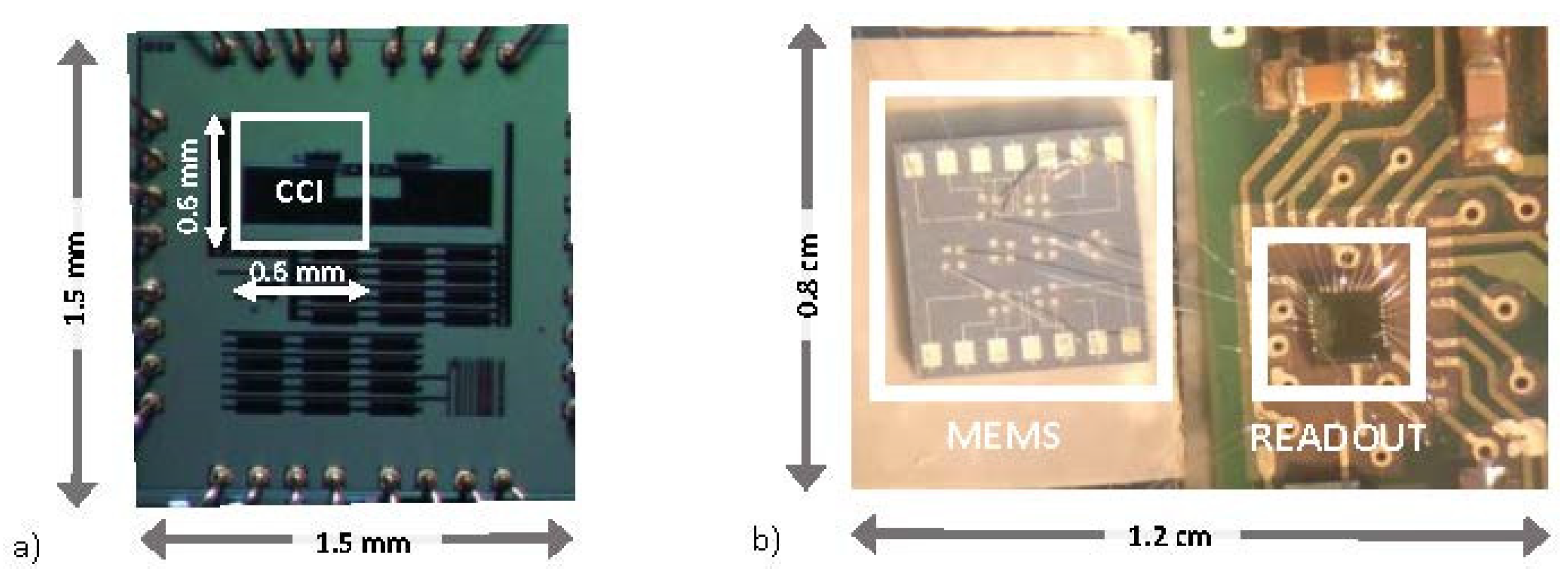
3.1. CMOS Prototype
The proposed circuit was implemented in a standard 0.18-µm technology and occupies about 0.4 mm2 (Figure 3a). The ASIC was mounted by chip-on-board technique to a test PCB and directly bonded to the DETF MEMS chip (Figure 3b). The CCI is supplied at 1.8 V and requires a stable and voltage reference VR = 0.9 V. The DETF is biased at VDC = 3.3 V. The typical static power consumption of the proposed readout circuit is 16 µW (9 µA at 1.8 V).
Figure 3.
(a) Microphotograph of the ASIC embedding the CCI-based sustaining amplifier (b) Photo of the ASIC directly bonded to the DETF.
3.2. Preliminary Tests on the CCI-DETF Strain sensor
The output of the global oscillator is a square wave voltage generated by connecting the Z node to a comparator (Figure 4a). This square wave oscillates at the resonance frequency of the DETF since the current on node Z equals the current on node Y. The bias voltage VDC of the DETF was varied from 2.4 V to 5 V to assess the correct locking of the oscillator to the resonant frequency f0. In fact, the resonance frequency of the DETF is inversely proportional to the applied electrostatic force while the feed-through capacitance is invariant to the applied electrostatic force [1]. The result of the measurement is shown in Figure 4b, in agreement with tests performed on the stand-alone DETF [1]. Another way to assess the correct locking at the resonant frequency of the DETF is by measuring the Allan deviation of the oscillation frequency. The high-quality factor Q of the DETF implies low values for the Allan deviation since most of the phase noise is filtered out by the DETF. On the contrary, if the readout amplifier locks with the feed-through capacitance at frequency fC then the resulting oscillation frequency will not be stable, showing a higher Allan deviation. Figure 4c shows the Allan deviation estimated on the square wave voltage after the comparator. The estimated Allan deviation is as low as 1 ppm at 20 ms, which demonstrates the correct locking and proves the low noise operation of the readout amplifier.
Figure 4.
(a) Output square wave whose frequency matches the resonance frequency of the DETF, in this case the natural resonance frequency is approximately 362 kHz. (b) Variation of the oscillation frequency due to changes in the applied VDC. (c) Estimated Allan deviation.
4. Conclusions
This paper presented a low-power and low-noise readout amplifier specifically designed for DETF resonators used as strain sensors. The proposed amplifier exploits current-domain design and weak-inversion operation to minimize the number of active elements, the noise, and the power consumption. Preliminary tests on a realized prototype demonstrate the correct functionality of the oscillator, which reported a power consumption as low as 16 µW and an Allan deviation of 1 ppm with 20-ms averaging time. Further tests comprise strain measurements and analyses of both the parasitic effects (like feed-through capacitance) and influencing quantities (like temperature).
Conflicts of Interest
The authors declare no conflict of interest.
References
- Belsito, L.; Ferri, M.; Mancarella, F.; Masini, L.; Yan, J.; Seshia, A.A.; Soga, K.; Roncaglia, A. Fabrication of high-resolution strain sensors based on wafer-level vacuum packaged MEMS resonators. Sens. Actuators A Phys. 2016, 239, 90–101. [Google Scholar] [CrossRef]
- Do, C.D.; Erbes, A.; Yan, J.; Soga, K.; Seshia, A.A. Vacuum Packaged Low-Power Resonant MEMS Strain Sensor. J. MEMS 2016, 25, 851–858. [Google Scholar] [CrossRef]
- Ferri, G.; Guerrini, N.C. Low-Voltage Low-Power CMOS Current Conveyors; Kluwer Academic Publishers: Dordrecht, The Netherlands, 2003. [Google Scholar]
- Enz, C.C.; Vittoz, E.A. CMOS low-power analog circuit design. In Proceedings of the Emerging Technologies: Designing Low Power Digital Systems, Montere, CA, USA, 12–14 August 1996; pp. 79–133. [Google Scholar]
Publisher’s Note: MDPI stays neutral with regard to jurisdictional claims in published maps and institutional affiliations. |
© 2018 by the authors. Licensee MDPI, Basel, Switzerland. This article is an open access article distributed under the terms and conditions of the Creative Commons Attribution (CC BY) license (https://creativecommons.org/licenses/by/4.0/).