Abstract
Transferable substrate-less InGaN/GaN light-emitting diode (LED) chips have successfully been fabricated in a laser lift-off (LLO) process employing high power ultrashort laser pulses with a wavelength of 520 nm. The irradiation of the sample was conducted in two sequential steps involving high and low pulse energies from the backside of the sapphire substrate, which led to self-detachment of the GaN stack layer without any additional tape release procedure. To guarantee their optoelectrical function and surface quality, the lifted LED chips were assessed in scanning electron microscopy (SEM) and electroluminescence (EL) measurements. Moreover, surface characterizations were done using atomic force microscopy (AFM) and Auger Electron Spectroscopy (AES).
1. Introduction
Gallium nitride (GaN) is a versatile semiconductor material that can be used to create LED devices for many different applications, including solid-state lighting and sensors. By transferring the nanostructured GaN LEDs onto flexible substrates, they could even exhibit enhanced performance compared to flexible organic LEDs in terms of their flexibility, longevity, and external quantum efficiency (EQE) [1]. Consequently, flexible inorganic LED devices have nowadays attracted more attention and possess potential to obtain novel functionalities (e.g., in optogenetics and biosensing applications) [2]. For the transfer of GaN LEDs from their original sapphire (Al2O3) substrate to other desired substrates, LLO has been developed and regularly used in the production of power LEDs as a reliable and reproducible technology. In a conventional LLO process, photons with energies above the band gap of GaN are normally used, so that the energy is dissipated at the sapphire/GaN interface [3]. These LLO processes are based on the expensive excimer laser technology. Alternatively, using femtosecond laser pulses with an extremely high density of photons allows for an induced multiphoton absorption, although the photon energy is lower than the semiconductor band gap [4]. In this work, a femtosecond LLO technology is proposed and the realization of free-standing blue GaN LED chips is demonstrated, which can potentially be employed for flexible device applications.
2. Material and Methods
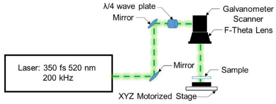
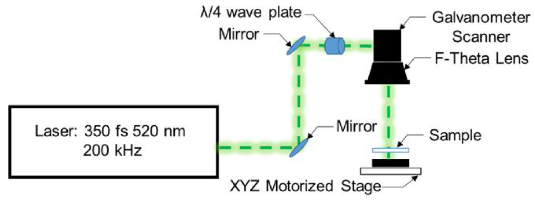
The employed laser for LLO process emits at a wavelength of 520 nm, a pulse length of 350 fs, and a repetition rate of 200 kHz for the optical system as seen in Figure 1. The micromachining system consists of a galvanometer scanner, with 100 mm focal length telecentric f-theta lens integrated with linear motorized XYZ positioning stage system, which can control the sample position and working distance between the objective and the workpiece. The laser beam polarization qualities were kept by a λ/4 wave plate in this optical system. In this experiment, InGaN/GaN LED epitaxial layers on 2″ sapphire substrates from epitaxy competence center (ec2) are used, consisting of 4.4 μm heavily doped n-GaN layer in the range of 1018–1019 cm−3, 4 pairs of InGaN/GaN multi quantum wells (MQWs) and p-GaN with a total thickness of approximately 300 nm. The LED epi-layers were grown by MOVPE on 420 μm thick, non-patterned, double-side polished sapphire substrates.

Figure 1.
Optical setup of femtosecond laser lift-off (LLO) system.
The main process of LLO is scanning of a laser beam across the backside of the sapphire substrate to separate the whole GaN LED layer without tape release. Although the impinging photons from the laser have lower energy (2.3 eV) than the GaN band gap (3.4 eV), the directed laser pulse has a high density of photons and is transmitted through the sapphire to reach the interface between the n-GaN layer and sapphire, where it is absorbed by a non-linear two-photon excitation process. In this approach, the LED selective area release was performed using a two-step LLO process with different laser energies as illustrated in Figure 2a–c.

Figure 2.
(a) Sketch of InGaN/GaN LED wafer. LLO process flow using two-step laser ablation from backside showing (b) material removal with high laser fluence for selectively creating the outer frame surrounding the to-be-lifted-off GaN chip and (c) scanning with lower laser fluence for releasing the GaN chip from the sapphire substrate.
At the laser focus position, the beam is too small and the intensity is too high for lift-off [3]. Thus, the size of the beam was adjusted by moving the sample towards the objective lens until reaching a defocused position at the sapphire/GaN interface. In this case, the LLO process comprises two-step laser irradiation. The first step defines the GaN LED chip by irradiating the perimeter or frame on a 2 × 2 mm2 area having a width of 0.5 mm from the outer line with a laser fluence of about 30 J/cm2 as shown in Figure 2b. To freely release an LED chip area of 1 × 1 mm2 from the sapphire substrate, the GaN LED was scanned with a lower laser fluence of 4.4 J/cm2 (Figure 2c). The final result from the processes is a free-standing GaN LED chip, whose n-GaN surface was afterwards investigated by SEM (Figure 3).

Figure 3.
SEM images of a lifted LED chip. (a) After selective outer frame removal of the GaN layer at high pulse energy, (b) lifted free-standing GaN/InGaN LED chip, (c) closer view at the n-GaN surface condition, (d) cross-section at a cut through the chip.
3. Results and Discussion
Concerning the experimental results, InGaN/GaN LED chips with a total area of 1 × 1 mm2 were successfully separated from the sapphire substrate in a reproducible process. Results from an LLO process of a free-standing GaN chip without transfer substrate and tape release are depicted in Figure 3.
Figure 3a shows an SEM image of a GaN LED wafer after selective outer frame removal by high laser fluence irradiation and remaining intact GaN LED in the middle of the area. After irradiating the intact GaN LED area with lower laser fluence, the GaN LED chip has been lifted and exhibited a crack-free p-GaN surface of the LED chip as seen in Figure 3b. On the other side, the n-GaN surface was affected by laser ablation resulting in marks on the surface (Figure 3c). To investigate the condition of the epilayer quality after LLO, we cut through the GaN LED chips and measured the thickness. From the cross-sectional view, a thickness of ~4.6 μm is observed, showing that the GaN LED epilayer is still complete and less damaged (Figure 3d). However, the n-GaN surface after LLO is relatively rough. Therefore, it has been investigated by AFM and AES (Figure 4a–c).

Figure 4.
Surface characterization n-GaN surface after LLO (a) 3D AFM profiles of n-GaN surfaces (b) SEM images of sample and the AES survey spectra of n-GaN surface with a spot size of 400 nm and (c) EL measurement result using probing tip setup.
Figure 4a shows typical AFM images of the LLO-based n-GaN chip surfaces. From roughness measurements, the average and root mean square (RMS) roughnesses of the n-GaN surfaces were found to be in the 100 nm to 150 nm, with maximum height of the profile up to 0.5 μm. The RMS values are still comparable with the value of LLO using nanosecond laser reported by Xiaoying et al. (i.e., 50 nm) [5]. However, it should be noted that when the lifted chip needs to be transferred onto another foreign substrate, the produced roughness on its surface can still affect the bonding quality. As the surface chemical composition of the detached n-GaN layer becomes important [6], AES measurements were also conducted. The AES spectrum (Figure 4b) can be explained by a gallium surface oxide, while Al2O3 residues on the surface could not be detected. Presumably, the air-exposed GaN surface has been oxidized and also contaminated with carbon- containing species after the lift-off. The results from AFM and AES measurements indicate that the surface conditions of the LED chips need to be improved for a subsequent transfer to flexible substrates. In this case, short-time wet chemical etching treatment could be a candidate for solution to smoothen the surfaces [7]. To ensure the functionality of the LED chip after laser ablation, EL measurement has been performed. Regardless of the poor contacts between the probing needles with the sample, it is obvious that the chip could still emit the blue light (Figure 4c). Further improvements of the LLO process and chip transfer are foreseen.
4. Conclusions
We successfully separated ~4.6 μm thin InGaN/GaN LED chips from their sapphire substrate by a selective LLO technique with 520 nm femtosecond laser pulse irradiation. In this technique, two- step laser scanning with high and lower laser fluence 30 J/cm2 and 4.4 J/cm2, respectively, has been applied to release 1 × 1 mm2 GaN LED. The AFM measurement after LLO shows that the n-GaN surface was relatively rough with an RMS roughness of ~150 nm. Further optimization of the lift-off process is therefore necessary to obtain smoother GaN surfaces suitable for transfer onto flexible substrates for various sensor applications.
Funding
This work has been partially performed within LENA-OptoSense funded by the Lower Saxony Ministry for Science and Culture (N-MWK) and European project of ChipScope funded by the European Union’s Horizon 2020 research and innovation program under grant agreement No. 737089.
Acknowledgments
The author would like to thank S. Fündling, K.-H. Lachmund, A. Schmidt, J. Breitfelder, and M. Rühmann for technical support in epitaxy competence center (ec2) and laboratories. N.Y. and N.M. thank the Ministry of Research, Technology and Higher Education of the Republic of Indonesia (RISTEKDIKTI) for the Ph.D. scholarship of RISET-Pro Loan No. 8245-ID and the Indonesian-German Centre for Nano and Quantum Technologies (IG-Nano) for the support.
Conflicts of Interest
The authors declare no conflict of interest. The funders had no role in the design of the study; in the collection, analyses, or interpretation of data; in the writing of the manuscript, and in the decision to publish the results.
References
- Guan, N.; Dai, X.; Babichev, A.V.; Julien, F.H.; Tchernycheva, M. Flexible inorganic light emitting diodes based on semiconductor nanowires. Chem. Sci. 2017, 8, 7904. [Google Scholar] [CrossRef]
- Seo, J.H.; Li, J.; Lee, J.; Gong, S.; Lin, J.; Jiang, H.; Ma, Z. A simplified method of making flexible blue LEDs on a plastic substrate. IEEE Photonics J. 2015, 7, 1–7. [Google Scholar] [CrossRef]
- Kim, J.; Kim, J.H.; Cho, S.H.; Whang, K.H. Selective lift-off of GaN light-emitting diode from a sapphire substrate using 266-nm diode-pumped solid-state laser irradiation. Appl. Phys. A Mater. Sci. Process. 2016, 122, 305. [Google Scholar] [CrossRef]
- He, F.; Liao, Y.; Lin, J.; Song, J.; Qiao, L.; Cheng, Y.; Sugioka, K. Femtosecond laser fabrication of monolithically integrated microfluidic sensors in glass. Sensors 2014, 14, 19402–19440. [Google Scholar] [CrossRef] [PubMed]
- Xiaoying, Z.; Yujiao, R.; Songyan, C.; Cheng, L. GaN/metal/Si heterostructure fabricated by metal bonding and laser lift-off. J. Semicond. 2009, 30, 123001-1–123001-4. [Google Scholar] [CrossRef]
- Wang, T.; Guo, X.; Fang, Y.; Liu, B.; Shen, G. Integration of GaN thin films with silicon substrates by fusion bonding and laser lift-off. Chin. Opt. Lett. 2006, 4, 416–418. [Google Scholar]
- Youtsey, C.; McCarthy, R.; Reddy, R.; Forghani, K.; Xie, A.; Beam, E.; Wang, J.; Fay, P.; Ciarkowski, T.; Carlson, E.; et al. Wafer-Scale Epitaxial Lift-off of GaN Using Bandgap-Selective Photoenhanced Wet Etching. Phys. Status Solidi B Basic Res. 2017, 254, 1600774. [Google Scholar] [CrossRef]
Publisher’s Note: MDPI stays neutral with regard to jurisdictional claims in published maps and institutional affiliations. |
© 2018 by the authors. Licensee MDPI, Basel, Switzerland. This article is an open access article distributed under the terms and conditions of the Creative Commons Attribution (CC BY) license (https://creativecommons.org/licenses/by/4.0/).


