Proceeding Paper

UV-LED Photo-Activated Room Temperature NO2 Sensors Based on Nanostructured ZnO/AlN Thin Films †

1
Institute of Semiconductor Technology (IHT), TU Braunschweig, 38106 Braunschweig, Germany
2
Laboratory for Emerging Nanometrology (LENA), TU Braunschweig, 38106 Braunschweig, Germany
3
MIND-IN2UB, Department of Electronic and Biomedical Engineering, University of Barcelona, 08007 Barcelona, Spain
4
Research Center for Physics, Indonesian Institute of Sciences (LIPI), Tangerang Selatan 15314, Indonesia
5
Institut für Energieforschung und Physikalische Technologien (IEPT), TU Clausthal, 38678 Clausthal, Germany
*
Authors to whom correspondence should be addressed.
Presented at the Eurosensors 2018 Conference, Graz, Austria, 9–12 September 2018.
Proceedings 2018, 2(13), 888; https://doi.org/10.3390/proceedings2130888
Published: 11 February 2019
(This article belongs to the Proceedings of EUROSENSORS 2018)

Abstract

:
UV-light emitting diodes (395–278 nm) were used to investigate the gas sensing attributes of planar and nanostructured ZnO/AlN thin films on Si substrate towards NO2 at room temperature. A significant increased sensitivity ((Rg − Ra)/Ra = 65.3 ppm NO2 in air) and a strong reduction in recovery time (Trec = 14 min) were already observed for the planar ZnO/AlN thin films under UV-B (305 nm) irradiation compared to the other UV wavelengths, while the device showed no obvious response in dark. By enlarging the surface-to-volume ratio of the sensors (i.e., creating nanostructured ZnO/AlN thin films), an increased response time is expected to be observed.

1. Introduction

Photo-activation is an obvious choice to lower the working temperature of metal oxide semiconductor based conductometric gas sensors. A reduction of required thermal activation energy will have a positive effect on lifetime and long-term stability of sensing performance, which is an inherent issue of solid-state gas sensor and an important research aim [1]. It also enables sensor application in the detection of flammable or explosive analytes and a significant reduced energy consumption for ubiquitous sensing in wearable devices. However, differentiating from the other handheld environmental sensors (e.g., airborne nanoparticle detectors [2,3,4]), conductometric gas sensors have to be activated either using illumination or thermal sources at room temperature to function [5]. Moreover, since the sensitivity of photo-activated gas sensors is generally quite low compared to conventional thermal energy activated sensors, 1D nanostructures and nanoporous sensing materials (e.g., zinc oxide (ZnO)) have been used to obtain a higher surface-to-volume ratio and large surface area [1]. Furthermore, the sensing response of photo-activated ZnO nanowires at room temperature is less sensitive to humidity [6] and therefore can enhance the selectivity towards NO2 [7] compared to thermal activated nanowires. It can also be seen that the sensing characteristics were morphology dependent. Therefore, the purpose of this work is to investigate the morphology and wavelength dependencies of photo-activated ZnO nanowires at room temperature to obtain NO2 gas sensors with sufficiently high response for practical devices.

2. Working Principle

Conductometric gas sensors are attractive due to their advantages of simplicity in measurement setup and potential of miniaturization for portable devices. An n-type sensing material like ZnO nanowire increases its resistance due to the chemisorption and reaction of oxidizing NO2 gas molecules [1,2]. If ZnO is exposed to air, a depletion layer is formed due to oxygen molecule adsorption, which pulls electrons from the conduction band to form oxygen ion species on the surface. The photon energy of UV illumination is sufficiently high to surpass the band gap of ZnO (3.37 eV or 368 nm at room temperature), which hence generates electron-hole pairs. The photo-generated holes react with the oxygen ions on the surface to form oxygen molecules, which will consequently be desorbed from the surface of ZnO. As a result, a steady state with lower resistance is created by adsorbing new oxygen molecules, which capture the photoelectrons to form photo-induced oxygen ions. After reaching a highly reactive equilibrium of oxygen adsorption and desorption, added NO2 molecules block the spots for the oxygen molecules to further oxidize the surfaces, due to their five time higher electronegativity. At those areas, the depletion layer increases again. Hence, the conductive channel of the ZnO will pinch off, which can be measured as an increase in electrical resistance under this reaction. The recovery process is initiated by exposing the ZnO surface to air, as oxygen will take the NO2 spots again.

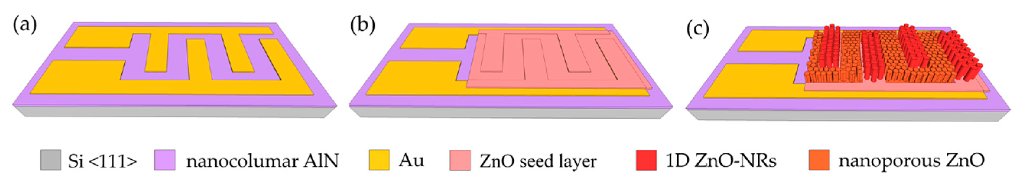
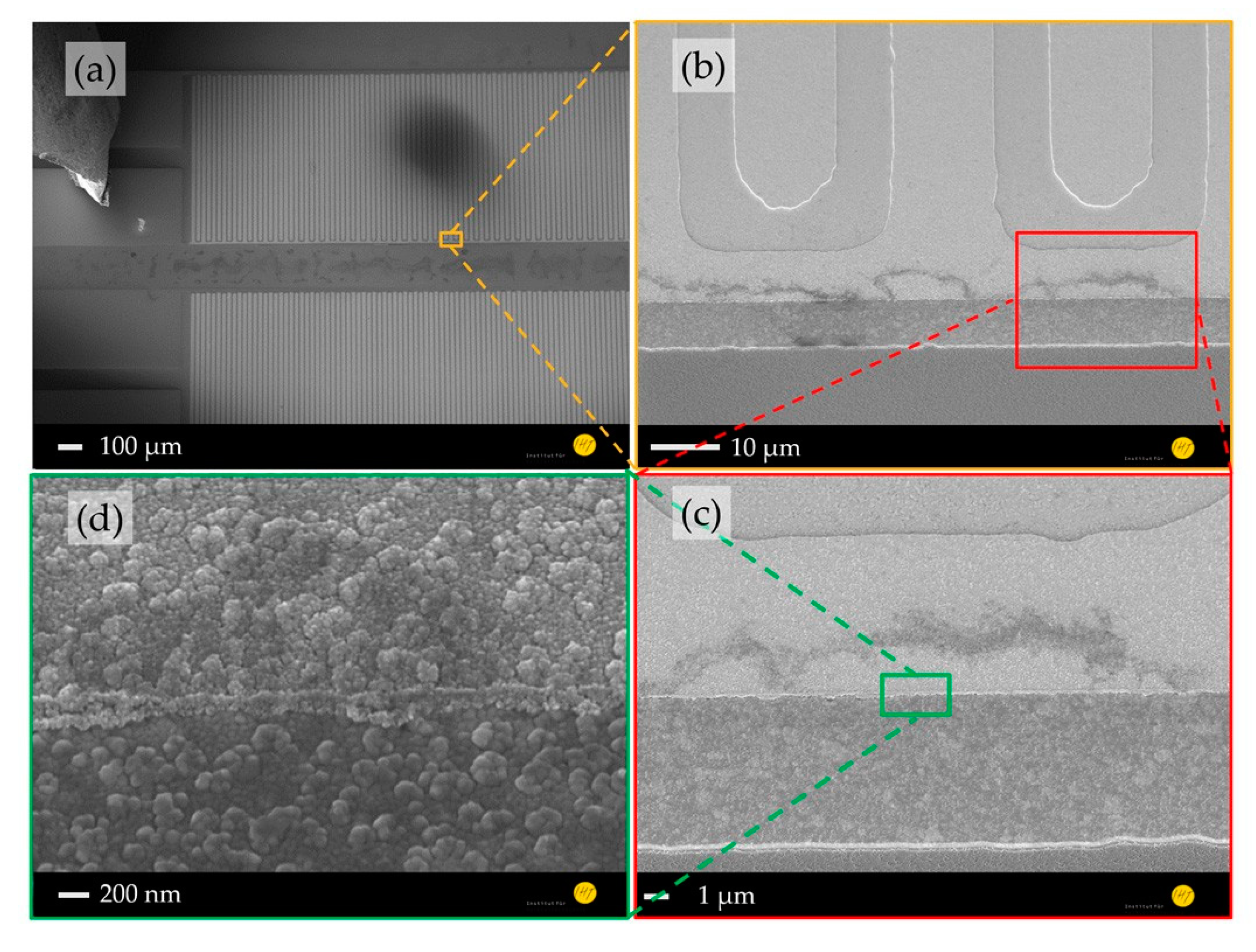
3. Sensor Fabrication

The sensor platform is composed of interdigitated electrodes (IDEs), which were fabricated on an AlN-on-Si layer grown by plasma vapor deposition of nano-columns (PVDNC) using photolithography and a subsequent lift-off process (Figure 1a). A total area of 800 × 1800 μm2 was designed for the electrode, in which an IDE width was set to be 15 μm. To deposit the sensing material, a ~300 nm ZnO seed layer was subsequently deposited in a Zn DC-sputtering process followed by oxidation in air at 300 °C (Figure 1b). By using a well-controlled chemical bath deposition (CBD), highly ordered 1D ZnO nanorods with a diameter of ~200 nm were realized on top of the Au electrodes, while their interstices were filled with ZnO nanoporous structures (Figure 1c).
A comparison between the morphologies of the planar (Figure 2) and nanostructured ZnO sensing layers (Figure 3) shows a significant increased surface-to-volume ratio. Furthermore, a structure transfer from the nanocolumnar AlN layer to the Au electrode and ZnO seed layer was observed (Figure 2d), which could cause the shape differences of the grown ZnO nanostructures on the Au electrodes and in their interstices (Figure 3c). The ZnO nanostructures between the IDEs are interconnected forming a high surface-to-volume-ratio nanoporous-networks throughout the electrodes, which are not necessarily given by the 1D NWs on top of the electrodes (Figure 3d). These ZnO networks provide a tremendous enlarged reactive surface for photo-activated molecule chemisorption compared to the planar layer, which is expected to enhance the device sensing performance.
Additionally, laser scanning microscopy (LSM) images reveal significant different growth rates between ZnO nanostructures grown on the ZnO seed layer covered Au electrodes and AlN layer, which result in varied heights of ~1.5 μm on the electrodes and ~4 μm in their interstices, respectively. This effect may be caused by the nanocrystalline quality of the AlN layer and different surface energies between those two basis materials. From the conducted atomic force microscopy (AFM) measurements, it was found that instead of having a monocrystalline AlN film across the whole substrate, the prepared sample was provided with millions of nanocolumns with a maximal height of ~60 nm. At this point, surface energy measurements still have to be carried out to further investigate the ZnO growth mechanism on those different materials (i.e., gold and AlN).

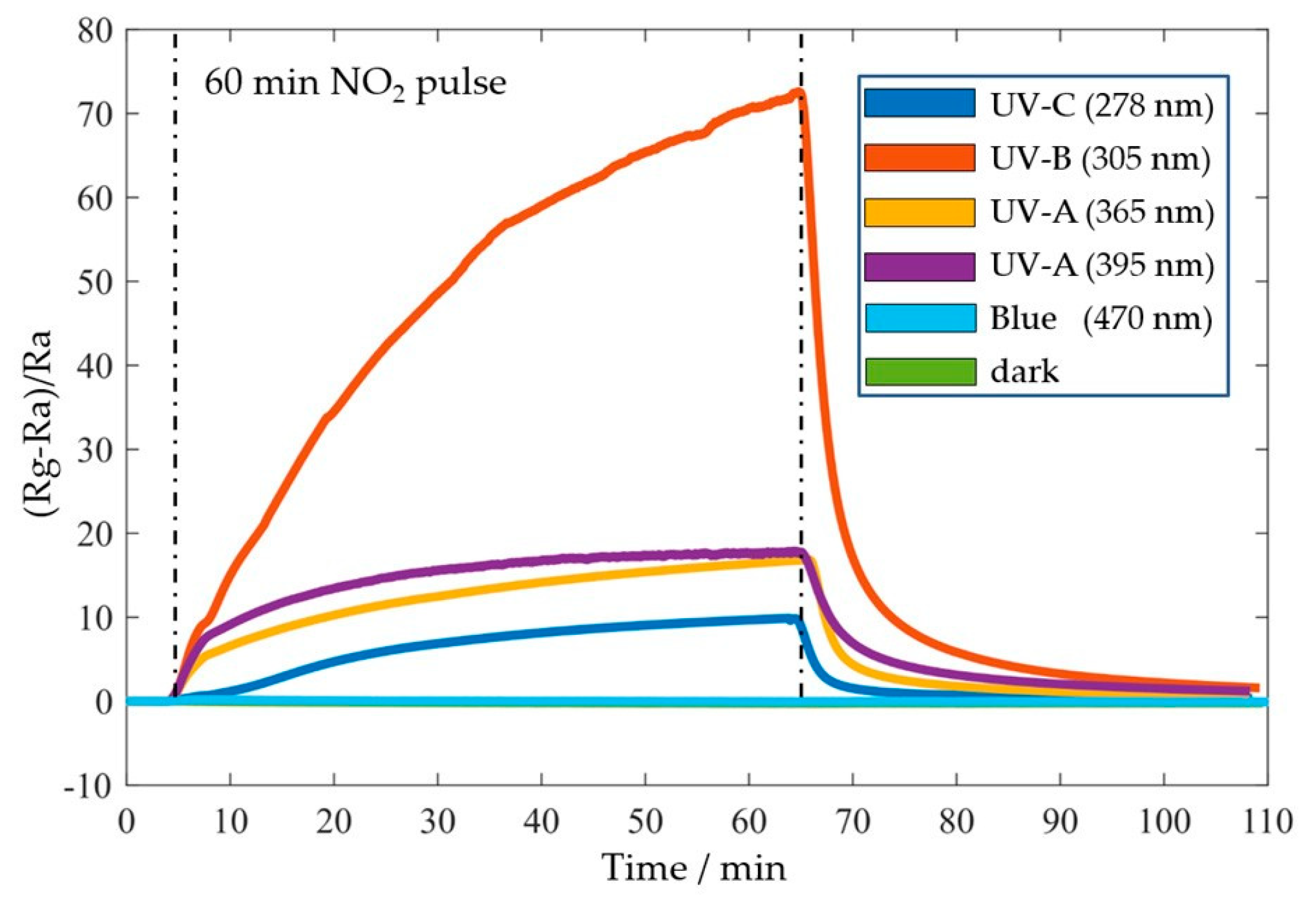
4. Measurement System and Results

Sensor performances were assessed in a homebuilt measurement system comprising a Keithley SMU 2614B, an MGP2 reference gas mixer, a hermetically sealed gas chamber, and a commercial environmental sensor next to the ZnO sensors for real-time monitoring of temperature, humidity, and pressure during gas measurements. For photo-activation, an integrated LED PCB assembled with ten different LEDs was stacked and placed ~1 cm above the sensors. The gas sensing characterization was performed using constant 1 V bias voltage with different UV-LED wavelengths (i.e., photon energies) above and below the ZnO bandgap energy. While dark and blue measurements showed no response, the resistance under UV illumination increases significantly with moderate rise and decay times. The best response (Rg - Ra)/Ra) of 65.3 at 5 ppm NO2 in air with a recovery time Trec of 14 min was obtained under UV-B (305 nm) illumination (Figure 4).

Author Contributions

T.G., M.T. and H.S.W. conceived and designed the experiments; T.G., M.T. performed the experiments; J.X. and E.P. produced ZnO layers and nanowires. T.G., M.T., Q., C.F., N.M., G.L., W.D., E.P., and H.S.W. analyzed the data and contributed reagents, materials, and analysis tools; T.G. wrote the paper; H.S.W. revised the paper; H.S.W. and A.W. lead the project funded by N-MWK.

Acknowledgments

The authors would like to thank A. Schmidt, J. Breitfelder, and M. Rühmann for their valuable technical assistance. This work is performed within project of LENA-OptoSense funded by the Lower Saxony Ministry for Science and Culture (N-MWK), Germany.

Conflicts of Interest

The authors declare no conflict of interest.

References

  1. Fabrega, C.; Casals, O.; Hernandez-Ramirez, F.; Prades, J.D. A review on efficient self heating in nanowire sensors: Prospects for very-low power devices. Sens. Actuators B 2018, 256, 797–811. [Google Scholar] [CrossRef]
  2. Wasisto, H.S.; Uhde, E.; Peiner, E. Enhanced performance of pocket-sized nanoparticle exposure monitor for healthy indoor environment. Build. Environ. 2016, 95, 13–20. [Google Scholar] [CrossRef]
  3. Wasisto, H.S.; Merzsch, S.; Uhde, E.; Waag, A.; Peiner, E. Handheld personal airborne nanoparticle detector based on microelectromechanical silicon resonant cantilever. Microelectron. Eng. 2015, 145, 96–103. [Google Scholar] [CrossRef]
  4. Wasisto, H.S.; Merzsch, S.; Waag, A.; Uhde, E.; Salthammer, T.; Peiner, E. Airborne engineered nanoparticle mass sensor based on a silicon resonant cantilever. Sens. Actuator B 2013, 180, 77–89. [Google Scholar] [CrossRef]
  5. Zhu, L.; Zeng, W. Room-temperature gas sensing of ZnO-based gas sensor: A review. Sens. Actuators A 2017, 267, 242–261. [Google Scholar] [CrossRef]
  6. Procek, M.; Pustelny, T.; Stolarczyk, A. Influence of external gaseous environments on the electrical properties of ZnO nanostructures obtained by a hydrothermal method. Nanomaterials 2016, 6, 227. [Google Scholar] [CrossRef] [PubMed]
  7. Zhang, S.; Lei, T.; Li, D.; Zhang, G.; Xie, C. UV light activation of TiO2 for sensing formaldehyde: How to be sensitive, recovering fast, and humidity less sensitive. Sens. Actuators B 2014, 202, 964–970. [Google Scholar] [CrossRef]
Figure 1. Sensor fabrication process steps: (a) deposition of Au layer; (b) ZnO seed layer deposition; (c) growth of ZnO nanorods and nanoporous-networks.
Proceedings 02 00888 g001
Figure 2. SEM images of gas sensor platform comprising planar ZnO/AlN thin films: (a) whole device, (b) electrode area covered by a ZnO seed layer, (c) layer stack of AlN/Au-electrode/ZnO, and (d) ~300 nm ZnO seed layer on an Au electrode.
Proceedings 02 00888 g002
Figure 3. SEM images of gas sensor platform consisting of ZnO nanorods on an AlN thin film: (a) whole device, (b) electrode area, (c) interstice between two ZnO-nanorod-covered Au-electrodes filled with nanoporous ZnO, and (d) highly ordered ZnO nanorods with a diameter of ~200 nm on an Au electrode.
Proceedings 02 00888 g003
Figure 4. Sensing response of a 2D ZnO/AlN thin film sensor at room temperature on 5 ppm NO2 in dark and under photo-activation with UV wavelengths and blue light.
Proceedings 02 00888 g004
Publisher’s Note: MDPI stays neutral with regard to jurisdictional claims in published maps and institutional affiliations.

