Abstract
We present a novel thermopile-based infrared (IR) sensor array fabricated on a single CMOS dielectric membrane, comprising of poly-silicon p+ and n+ elements. Processing of the chip is simplified by fabricating the entire array on a single membrane and by using standard CMOS Al metal layers for thermopile cold junction heatsinking. On a chip area of 1.76 mm × 1.76 mm, with a membrane size of 1.2 mm × 1.2 mm, we fabricated IR sensor arrays with 8 × 8 to 100 × 100 pixels. The 8 × 8 pixel device has <2% thermal crosstalk, a responsivity of 36 V/W and enhanced optical absorption in the 8–14 µm waveband, making it particularly suitable for people presence sensing.
1. Introduction
Low-cost IR image sensors are increasingly used for a variety of applications, ranging from home appliances and security to automotive and IR cameras for smartphones [1]. These sensors typically consist of an array of thermopiles or bolometers, with the former being inherently insensitive to changes in ambient temperature [1] and being easier to manufacture using low-cost Complementary Metal–Oxide–Semiconductor (CMOS) fabrication processes [2,3], which makes the technology more attractive for commercialization. Thermopile sensors detect a temperature difference ∆T across each thermopile element and are composed of several thermocouples with their hot junctions thermally isolated, typically by a thin dielectric membrane [4,5]. When the membrane is heated by incident IR radiation, a voltage VT = Nα∆T is generated due to the Seebeck effect [5] which is proportional to the temperature difference across the thermocouple elements ∆T, the Seebeck coefficient α and the number of thermocouples N. The responsivity ℜ is defined as the change in voltage response due to incident optical power (ℜ = dVT/dP) and is highly dependent on the thermal resistance of the device [5]. Micromachining of the silicon substrate can be used to form a membrane with a high thermal resistance to enhance IR heating and thus responsivity [2,3]. A typical array consists of thermopile pixel elements, each fabricated on an isolated membrane, formed by bulk etching of the substrate [1,4]. However, this fabrication method requires critical process control to minimize substrate etching tolerances and undercut. IR thermopile arrays fabricated on a single membrane have been reported but employ non-standard structures above or below the membrane. Examples include bulk silicon layers [6] or additional gold layers [7] acting as heatsinks. Gold is not fully CMOS compatible, which results in non-standard processes and increased fabrication costs [3].
Here we present a CMOS based thermopile array fabricated on a single membrane, employing standard CMOS Al layers for heatsinking of thermopile cold junction elements; a design which simplifies chip processing.
2. Device Fabrication
Our thermopile arrays were fabricated using a commercial 0.35 μm CMOS process on 6 inch Si wafers. Four devices, having array sizes of 8 × 8, 24 × 24, 60 × 60 and 100 × 100 pixels, were fabricated as a proof of concept. The pixels are formed by highly doped p+ and n+ poly-Si layers with sheet resistances of 153 Ω/□ and 184 Ω/□ respectively. The interconnects between the poly-Si p+ and n+ elements, and the heatsinking tracks between the pixels are formed by three Al interconnect layers, with track widths of 20 μm and thicknesses of 0.4 μm, 0.4 μm and 0.8 μm, respectively (for the 8 × 8 pixel sensor). The SiO2 based membrane has an area of 1200 μm × 1200 μm and is ~5 μm thick, see Figure 1. The layers were grown on a 375 μm thick Si substrate which was back-etched using Deep Reactive Ion Etching (DRIE) to form the membrane, with the first SiO2 layer acting as an etch stop. The individual pixels consist of 36 thermocouples with their cold junctions placed adjacent to the surrounding heatsinking tracks, formed by the three Al layers.
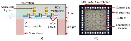
Figure 1.
(a) Cross-sectional view showing the p+/n+ poly-Si and Al layers of the thermopile array; (b) Optical image of the thermopile array. Chip size = 1.76 mm × 1.76 mm.
3. Results and Discussions
For measurement purposes, we mounted the device in an open surface mount Quad-Flat No-leads (QFN) type package with the individual pixels electrically bonded. The active pixel elements were addressed using a multiplexer and amplified and digitized using an analogue-front-end integrated circuit (LMP93601), interfaced to an Arduino microcontroller board. The test setup is illustrated in Figure 2. For responsivity tests, the device was mounted at a distance of 50 mm from a blackbody source (Fluke 4180) which was held at a constant temperature of 100 °C.
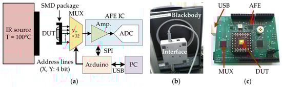
Figure 2.
IR detector array: (a) Schematic; (b) Characterization setup; and (c) Circuit board interfacing.
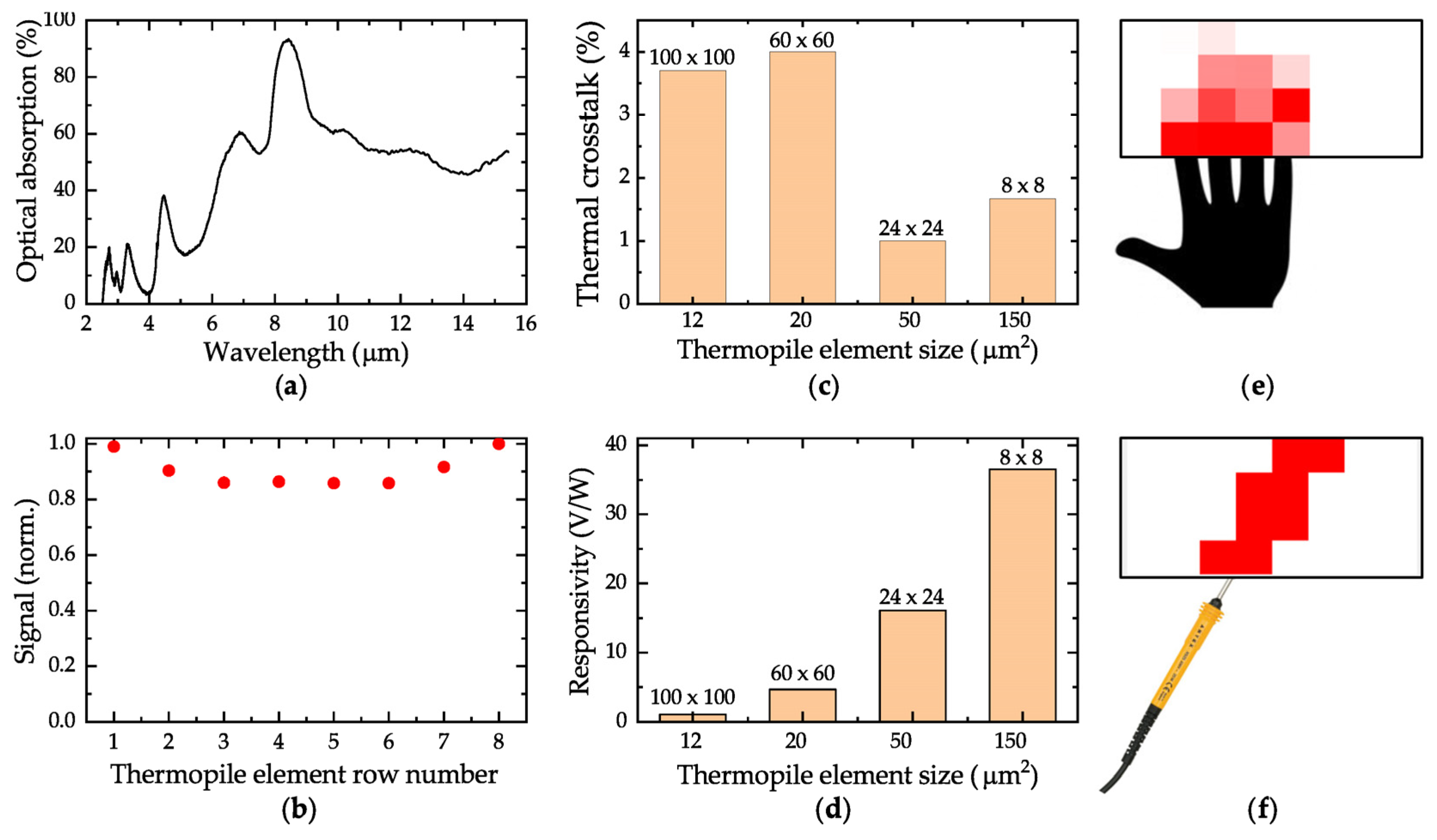
The thermopile detector shows enhanced optical absorption in the 8–14 μm waveband (measured using a FTIR spectrometer) with an absorption peak of ~90% at 8.5 μm (see Figure 3a), making it suitable for people presence detection [8]. Optical absorption can be further enhanced by the addition of a high emissivity coating e.g., gold black layer, at the expense of an extra processing step [2]. The uniformity of response to IR illumination per pixel for the 8 × 8 pixel array is shown in Figure 3b. Pixel elements in the center of the membrane show a maximum 15% drop in signal level due to the lower efficiency of the thermopile cold junction heatsinking. At the edge of the membrane, the substrate acts as a more efficient heatsink, maximizing ΔT between the hot and cold junctions, thereby creating a higher VT. Responsivity non-uniformity could be compensated for by external gain compensation e.g. by using an Application-Specific Integrated Circuit (ASIC). The cross-sensitivity of the sensor (a measure of the crosstalk between the pixels) was measured by electrically heating an individual pixel using an embedded micro-heater and measuring VT for both the heated and adjacent pixels. This is shown in Figure 3c for arrays with differing numbers of pixels. The 8 × 8 and 24 × 24 arrays show low thermal crosstalk (<2%); demonstrating the efficiency of the heatsinking between pixels. Arrays with smaller pixels show increased thermal crosstalk (>3.5%) due to increased thermal leakage, as the thermal path between pixels is reduced.

Figure 3.
(a) Infrared absorption spectrum of the 8 × 8 pixel array measured using FTIR spectroscopy; (b) Uniformity of optical response; (c) Thermal crosstalk between pixels; (d) Responsivity values; (e) Hand and (f) soldering iron images taken using the 8 × 8 pixel array at 1 m distance (32 pixels addressed).
The 8 × 8 pixel array has a ℜ of 36 V/W and a specific detectivity D* = of 9.5 × 106 cm Hz/W, where A is the membrane area, f the frequency bandwidth and NEP = Sn/ℜ the noise-equivalent power with Sn being the noise spectral density. Arrays with smaller pixel areas show a drop in ℜ due to the reduced conversion efficiency of each pixel, as shown in Figure 3d. ℜ could be further enhanced by vacuum packaging to minimize heat loss which would make higher resolution imaging possible [3].
To demonstrate the application of our sensor, thermal images of objects were acquired using an Umicore IR lens [focal length = 6.8 mm, f-number = 1.4, and field of view (FOV) = 8°] and are shown in Figure 3e,f. People presence detection was possible at a distance of 2 m and there was good contrast between pixel elements. A fuller range of specifications for our sensor is presented in Table 1.

Table 1.
Characteristics of the 8 × 8 pixel thermopile array.
4. Conclusions
A CMOS thermopile-based IR sensor array fabricated on a single SiO2 dielectric membrane, comprising of poly-Si p+ and n+ elements has been demonstrated. Processing of the chip is simplified by the use of a single membrane and standard CMOS Al layers for thermopile cold junction heatsinking. The 8 × 8 pixel array with 20 μm wide heatsinking tracks shows low crosstalk (<2%), enhanced optical absorption in the 8–14 μm band and has a responsivity of 36 V/W, making it suitable for people presence and gesture detection, in low cost applications. Vacuum packaging and high emissivity coating could be used to further enhance responsivity.
Author Contributions
Conceptualization, R.H., S.Z.A. and F.U.; Investigation, All; Writing, R.H. and D.P.
Funding
This research was funded by ams Sensors UK Limited.
Conflicts of Interest
The authors declare no conflict of interest.
References
- Kimata, M. Uncooled infrared focal plane arrays. IEEJ Trans. Electr. Electron. Eng. 2017, 13, 4–12. [Google Scholar] [CrossRef]
- Udrea, F.; Luca, A.D. CMOS technology platform for ubiquitous microsensors. In Proceedings of the 2017 International Semiconductor Conference (CAS), Sinaia, Romania, 11–14 October 2017; pp. 43–52. [Google Scholar]
- Baltes, H.; Brand, O. CMOS-based microsensors and packaging. Sens. Actuators A Phys. 2001, 92, 1–9. [Google Scholar] [CrossRef]
- Hopper, R.; Ali, S.; Chowdhury, M.; Boual, S.; De Luca, A.; Gardner, J.W.; Udrea, F. A CMOS-MEMS thermopile with an integrated temperature sensing diode for MID-IR thermometry. Procedia Eng. 2014, 87, 1127–1130. [Google Scholar] [CrossRef]
- Van Herwaarden, A.W.; Sarro, P.M. Thermal sensors based on the Seebeck effect. Sens. Actuator 1986, 10, 321–346. [Google Scholar] [CrossRef]
- Oliver, A.; Wise, K. A 1024-element bulk-micromachined thermopile infrared imaging array. Sens. Actuators A Phys. 1999, 73, 222–231. [Google Scholar] [CrossRef]
- Schaufelbuchl, A.; Munich, U.; Menolfi, C.; Brand, O.; Paul O. Huang, Q.; Baltes, H. 256-pixel CMOS-integrated thermoelectric infrared sensor array. In Proceedings of the 14th IEEE International Conference on Micro Electro Mechanical Systems Technical Digest (Cat. No.01CH37090) (MEMS 2001), Interlaken, Switzerland, 25–25 January 2001; Volume 48, pp. 47–54. [Google Scholar] [CrossRef]
- Zappi, P.; Farella, E.; Benini, L. Tracking Motion Direction and Distance with Pyroelectric IR Sensors. IEEE Sens. J. 2010, 10, 1486–1494. [Google Scholar] [CrossRef]
Publisher’s Note: MDPI stays neutral with regard to jurisdictional claims in published maps and institutional affiliations. |
© 2018 by the authors. Licensee MDPI, Basel, Switzerland. This article is an open access article distributed under the terms and conditions of the Creative Commons Attribution (CC BY) license (https://creativecommons.org/licenses/by/4.0/).