Proceeding Paper

Versatile and Automated 3D Polydimethylsiloxane (PDMS) Patterning for Large-Scale Fabrication of Organ-on-Chip (OOC) Components †

1
Laboratory of Electronic Components, Technology & Materials (ECTM), EKL, Delft University of Technology, Feldmannweg 17, 2628 CT Delft, The Netherlands
2
BIOND Solutions B.V., Mekelweg 4, 2628 CD Delft, The Netherlands
3
Besi Netherlands B.V., 6921 RW Duiven, The Netherlands
4
Philips Research, 5656 AE Eindhoven, The Netherlands
*
Author to whom correspondence should be addressed.
Presented at the Eurosensors 2018 Conference, Graz, Austria, 9–12 September 2018.
Proceedings 2018, 2(13), 873; https://doi.org/10.3390/proceedings2130873
Published: 5 December 2018
(This article belongs to the Proceedings of EUROSENSORS 2018)

Abstract

:
We present a reproducible process to directly pattern 3-Dimensional (3D) polydimethylsiloxane (PDMS) structures for Organ-on-Chips (OOC) via automated molding. The presented process employs a commercially available system from IC packaging improving the fabrication process for microfluidic channels and thin membranes, which are components frequently used in OOCs. The process removes the manual steps used previously in the fabrication of microfluidic channels and improves the control over the thickness of the PDMS layers. The process was also employed to fabricate and pattern thin PDMS membranes on silicon wafers, without the use of lithography and etching steps and in combination with 3D structures. The use of foil assisted molding techniques presented in this work is an important step toward the large-scale manufacturing of OOCs.

1. Introduction

Organ-on-Chips (OOC) are microfabricated devices, often composed of microfluidic channels and polymeric membranes assembled to create a dynamic microenvironment for cell culturing. The different kind of cells cultured on the chips are able to interact, creating an in vitro model of functional units of an organ. Growth, proliferation, differentiation, maturation and controlled interactions between the different cell types in the model are promoted by the dynamically controlled environment in the device [1,2].
The microfluidic channel and membranes included in these devices are often fabricated using polydimethylsiloxane (PDMS) patterned via soft lithography [3]. This allows simple and rapid modeling of new three-dimensional (3D) chips and is therefore particularly useful in rapid prototyping of new designs [1]. However, soft lithography is based on labor-intensive procedures that reduce device throughput and yield, a hurdle to large-scale fabrication.
The fabrication of the microfluidic channels with soft lithography is often performed by manually pouring a PMDS layer on top of a patterned silicon wafer. The only way to control the thickness of the layer is by adjusting the volume of uncured PDMS. Besides being unreliable, this method does not guarantee uniformity across the wafer.
On the other hand, previous works [4] have focused on improving the fabrication of the membranes using standard silicon-based fabrication techniques. In order to do this, the PDMS is spun-coated on a silicon wafer and patterned by means of standard photolithography and dry-etching. These steps are not fully optimized and standardized due to differences in thermal expansions, hydrophobicity, and swelling of the PDMS [4]. Moreover, the topographies achievable are quite limited in terms of thickness and aspect ratios, resulting in most of the time only in simple 2D features.
This work overcomes these limitations by combining standard silicon fabrication processes with automated 3D molding techniques using a commercially available molding system. With our technique, molded microfluidic channels can be fabricated without any manual dispensing, providing high control over the thickness. Moreover, the process was used to fabricate PDMS membranes on a silicon wafer including 3D topographies without the need for lithography or etching.

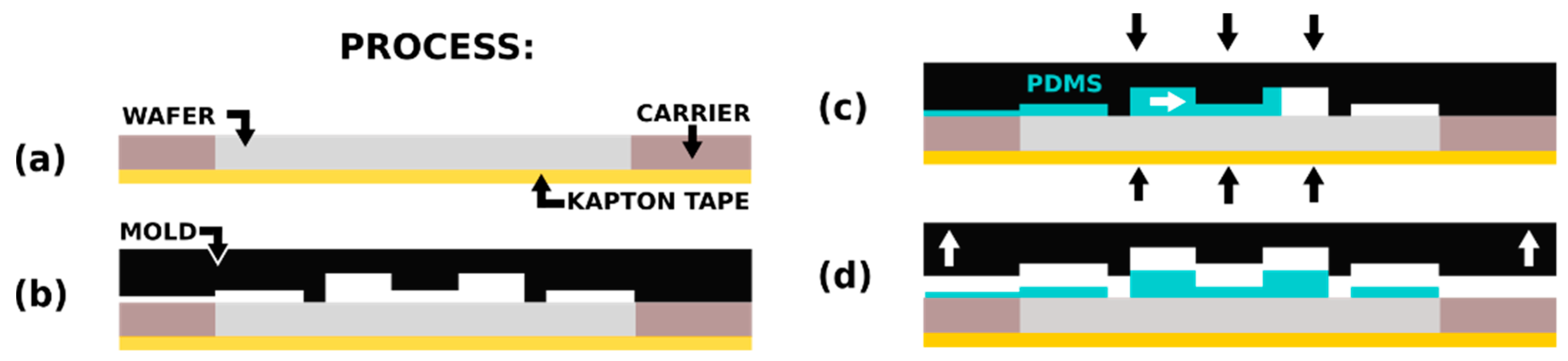
2. Automated 3D Molding on Silicon Wafers

The 3D PDMS molding on silicon wafers is performed using a commercially available BESI MMS-LM molding system. For this proof-of-concept, the wafer was diced and re-shaped in order to fit on top of a pre-existing holder (Figure 1a). The loading of the wafer is currently performed manually, but other BESI’s tools (e.g., an AMS-LM_molding system) perform this step automatically. The wafer can be either pristine or pre-processed in order to embed MEMS or electrical components and structures in the PDMS [4]. A pre-designed mold, with the negative image of the desired PDMS structure, is automatically brought in contact with the wafer (Figure 1b). During the process, the mold is protected from the injected polymer by means of a 50 µm thick Ethylene Tetra Fluoro Ethylene (ETFE) foil that is pulled and fixated to the inner surfaces of the mold by special vacuum channels.
Next, PDMS (Sylgard 182 with a 1:10 elastomer/curing agent ratio) is injected into the cavities of the mold creating the desired structures (Figure 1c). The pressure between the wafer and the mold is kept constant, preventing any damage to the wafer. Moreover, the injection speed is controlled to smoothly fill the mold with a transfer speed starting at 2 mm/s, slowing down to 1 mm/s and finally to 0.5 mm/s. The molding tool is equipped with a venting mechanism that mechanically closes as soon as the cavity is completely filled. After that, the temperature (100 °C) and the pressure (5 MPa) are kept constant for the time needed for pre-curing of the PDMS (10 min). After curing, the molding press opens and the molded sample is removed (Figure 1d). Finally, the wafer is manually removed from the holder, and fully cured (120 °C, 4 h). The automatic molding prevents PDMS residues or particles on the back and sides of the wafer, allowing for further processing of the wafer in a clean-room environment. The machine mold cleaning is automatically performed by removing the ETFE foil from the mold.

3. Fabrication of Organ-on-Chip Components

The process presented in Section 2 was employed to fabricate a microfluidic channel previously used for a Lung-on-Chip application [3] and a polymeric membrane previously used in a Heart-on-Chip [4].
The steps of the novel process applied for the fabrication of a microfluidic channel are presented in Figure 1a–c. For the fabrication of the microfluidic channels, a flat mold was used in order to deposit a uniform layer of PDMS on top of 100 µm-thick structures made of THB-151N negative photoresists (PR) (Figure 1a). The PR was conformally covered by the PDMS without any bubbles or voids formation, as shown in Figure 2b,d,e. The thickness of the PDMS can be changed by tuning the distance between the mold and the wafer in the machine. This guarantees a high control over the thickness of the molded layer across the wafer. By adjusting the distance between the wafer and the mold to 200 µm, it is possible to obtain a 200.8 µm layer with variations of only ± 4 µm, as measured with a Dektak 8 surface profilometer. The thickness of the PDMS layer can be easily increased up to 1 mm. The fabrication of the channels was finalized by peeling the PDMS layer from the wafer leaving the PR pattern transferred to the bottom side of the PDMS film (Figure 2c,f). The easy peeling of the layer is guaranteed by the poor adhesion between PDMS and the silicon wafer [5].
Furthermore, the process was also employed to fabricate the stretchable membranes included in the Heart-on-Chip presented by Gaio et al. [4]. The process allowed the fabrication of the membranes in one single step, without any need for lithography and etching steps to pattern the PDMS. The steps of the novel process applied for the fabrication of a membrane are shown in Figure 1a–c. A PDMS layer is molded on a pre-processed wafer as shown in Figure 3d. The process allowed depositing and patterning of 3D PDMS structures with thicknesses ranging from 15 to 175 µm, while leaving non-patterned areas of the wafer free from PDMS (Figure 3d,e). The thickness of the layer was characterized with a VK-X250 3D Laser Scanning Confocal Microscope, showing variations of only ±1.3 µm on the 15 µm-thick membrane areas across the wafer (Figure 3f). The 15 µm PDMS membranes were then released by etching the silicon supporting the PDMS membrane (Figure 3c,g,h) by means of Deep Reactive Ion Etching (DRIE). In order to do this, the molded wafer was turned upside down and loaded on a transport wafer. Reduction of the membrane thickness has not been attempted as it was foreseen that process stability would be affected.

4. Conclusions

We developed an automated and versatile process to obtain 3D PDMS structures on a silicon wafer for OOC applications. A detailed description of the PDMS deposition and patterning with a BESI MMS-LM system was reported. Subsequently, we applied the developed technology to fabricate two components often included in OOCs: microfluidic channels and thin membranes The results clearly indicate that this process can be effectively used in the microfabrication of multiple 2D and 3D structures, showing its versatility.
The microfluidic channels were fabricated by imprinting 100 µm thick PR structures in a 200 µm PDMS layer. The new processed improves the standard molding procedure. It is possible to control the thickness of the molded layer, avoiding any manual dispensing. Thin membranes (15 µm thick) were fabricated by molding a variable thickness layer on a silicon wafer and then selectively remove the silicon from underneath the PMDS. Unlike previous works [4], the deposition and patterning of this structure were performed in one single step, without the need for photo-lithography and etching.

Author Contributions

N.G., S.K., and R.D. conceived experiments. N.G. and S.K. performed and analyzed data. N.G., S.K., W.Q.S., P.L.S., and R.D. wrote the paper.

Acknowledgments

The authors would like to thank the Institute for Human Organ and Disease Model Technologies (hDMT). Moreover, the authors gratefully acknowledge the technical support and advice of the staff at the Else Kooi Laboratory (EKL). This work was performed in the framework of the ECSEL JU InForMed Project (grant no. 2014-2-662155).

Conflicts of Interest

The authors declare no conflict of interest

References

  1. Beißner, N.; Lorenz, T.; Reichl, S. Organ on chip. In Microsystems for Pharmatechnology; Springer: Cham, Switzerland, 2016; pp. 299–339. [Google Scholar]
  2. Van de Stolpe, A.; den Toonder, J. Workshop meeting report Organs-on-Chips: Human disease models. Lab Chip 2013, 13, 3449–3470. [Google Scholar] [CrossRef] [PubMed]
  3. Huh, D.; Matthews, B.D.; Mammoto, A.; Montoya-Zavala, M.; Hsin, H.Y.; Ingber, D.E. Reconstituting organ-level lung functions on a chip. Science 2010, 328, 1662–1668. [Google Scholar] [CrossRef] [PubMed]
  4. Gaio, N.; van Meer, B.; Quirós Solano, W.; Bergers, L.; van de Stolpe, A.; Mummery, C.; Sarro, P.M.; Dekker, R. Cytostretch, an organ-on-chip platform. Micromachines 2016, 7, 120. [Google Scholar] [CrossRef] [PubMed]
  5. Huh, D.; Kim, H.J.; Fraser, J.P.; Shea, D.E.; Khan, M.; Bahinski, A.; Hamilton, G.A.; Ingber, D.E. Microfabrication of human organs-on-chips. Nat. Protoc. 2013, 8, 2135–2157. [Google Scholar] [CrossRef] [PubMed]
Figure 1. Process flow: (a) the wafer is loaded on a customized holder and inserted in an MMS-LM molding system, (b) the mold, protected by a 50 µm EFTE foil, is brought in contact with the wafer, (c) the uncured PDMS is loaded inside the molding machine and is injected into the mold cavities, and (d) the molding press opens and the wafer is unloaded.
Proceedings 02 00873 g001
Figure 2. Process flow applied for the fabrication of microfluidic channel: (a) PR is deposited and patterned on a silicon wafer, (b) PDMS is molded on top of the PR structures with the presented process and (c) the PDMS structure is peeled-off from the wafer. (d) SEM images of the 100 µm thick photoresist (PR) structures embedded in a 200 µm thick PDMS layer. (e) Close-up of the PR structures covered with PDMS. The PDMS conformally covered the vertical walls of PR, thus retaining the predefined geometry. The microfluidic channels were created by peeling off the PDMS layer ending up with the photoresist pattern imprinted on the back of the PDMS layer (f).
Proceedings 02 00873 g002
Figure 3. Process flow applied for the fabrication of a membrane: (a) a pre-processed wafer with metallic and polymeric structures presented in [4] is used, (b) PDMS is molded on top of the structures with the presented process and (c) the PDMS membrane released by etching the silicon under the PDMS with DRIE. (d,e) Silicon wafer with 3D PDMS molded structures customized for the Heart-on-Chip presented by Gaio et al. [4]. The topographies and the thickness of the PDMS layer were analyzed and measured with SEM images (f) and Laser Scanner. The process allowed forming structures with different heights in a single step (ranging between 17 µm and 175 µm). Moreover, designated areas of the wafer are left completely clean from PDMS, thus avoiding any etching step. (g,h) Suspended PDMS areas/membranes were then released by locally etching the silicon from the back of the wafer with deep-reactive ion etching.
Proceedings 02 00873 g003
Publisher’s Note: MDPI stays neutral with regard to jurisdictional claims in published maps and institutional affiliations.

