Abstract
In this paper, a hybrid optical guiding system based on low group velocity offered by photonic crystal (PhC) waveguides and vertical confinement as well as high field enhancement of. Surface lasmon polaritons (SPP) is proposed. We show that for efficient sensing, conventional two-dimensional PhC waveguides with finite height require a high aspect ratio in the order of 30 in order to efficiently confine the guiding mode. The fabrication of devices with such a high aspect ratio is considered too challenging and inefficient for mass production. By combining a PhC waveguide and SPPs, the proposed system efficiently confines the optical mode vertically while benefiting from the lateral confinement enabled by PhC structures. As a result, the required aspect ratio drops to about 4 making the fabrication in large scale feasible. This design provides strong light-matter interaction within small dimensions, which is beneficial for miniaturizing on-chip photonic sensors.
1. Introduction
Plasmonic waveguides based on surface plasmon polaritons (SPPs) have served the optical region with their peculiar properties of confining light as well as controlling its energy propagation properties. properties. SPPs are the collective oscillations of free electrons in a metal interacting with photons at the metal-dielectric interface [1]. The oscillation is neither pure electric, nor pure photonic; as a result, the electromagnetic energy can be localized in the dimensions much smaller than the diffraction limit. This high field localization results in an efficient light-matter interaction. On the other hand, photonic crystals (PhCs) have long been a subject of interest due to their potential for versatile application in spatial and temporal control of light in micron and sub-micron scale devices [2]. A photonic crystal (PhC) is a periodically modulated refractive-index structure where the characteristic periodicity is the order of optical wavelength to be considered. Photonic crystals can possess a photonic band gap (PBG) under certain conditions, thus enabling it to function as a photonic insulator over a desired range of frequency [3]. In the present work, we use a pillar based photonic crystal waveguide with a schematic representation shown in Figure 1a. The 2-dimensional (2D) calculation of dispersion band diagram for TE polarization (electric field in z direction) is presented in Figure 1b, the shadowed region corresponds to the band gap of the system. For a waveguide functioning within the band gap frequency range, the photonic crystals play the role of a confining region. On the other hand, surface SPPs are commonly utilized in visible and near infrared optical sensing applications, thanks to their excellent light confinement and field enhancement properties. In this work, we bring these two well-known concepts together in order to address a common fabrication challenge, i.e., the high aspect ratio of pillars in conventional PhC waveguides needed to confine the mode of interest. We propose a design for the wavelength of 632 nm for which not only this challenge is tackled, but also the other dimensions of the system are reduced. The computations in this work have been performed using the commercial RSoft package based on Finite Difference Time Domain (FDTD) and COMSOL Multi physics based on the finite element method.
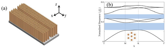
Figure 1.
(a) A 3D Schematic representation of a PhC waveguide formed by removing a row of pillars in a periodic arrays of Si pillars on SiO2 substrate. (b) Transverse electric band structure of a 2D hexagonal PhC made of Si pillars with the radius of r = 0.22a. The shadowed region represents the band gap of this structure. (Inset: schematic view of a 2D hexagonal lattice of Si pillars).
2. Sensor Based on Photonic Crystal Waveguide
In a PhC waveguide, when the frequency of the wave is close to the band edge of the dispersion diagram, the group velocity of the guided mode, defined as the derivative of the wavenumber with respect to the frequency, approaches zero, which means that the velocity of the guided energy becomes very small. The group velocity for propagating waves crucially affects the efficiency of the light-matter interaction: the lower the group velocity, the higher the intensity of photon-matter interaction [4]. For sensing applications, especially when the concentration of the analyte and its variation is low, efficient interaction between the analyte and light plays an important role; since it not only determines the dimension of the device, but also the sensitivity of the sensor [5].
Ideally, in order to have a full confinement of light inside the waveguide, 3-dimensional (3D) structures, such as 3D PhCs, are desirable. In such a structure, the confinement in the plane perpendicular to the propagation direction is supported by the 3D PhC lattice. Although such a design offers the best confinement and control over the properties of the guided wave, its realization in a fabrication process is either impossible or cumbersome especially for application where mass production is the goal. In this case, a common approach is to incorporate finite 2D structures with certain thickness in the vertical dimension. Finite 2D periodicity can be accomplished either by creating holes inside a slab or by forming pillars of a dense material (Figure 1a). While in the former case the vertical confinement along the z-axis is accomplished by total internal reflection of light, in the latter case, the pillars should be high enough to increase the overall effective refractive index of the guiding mode and therefore being able to confine the wave along the z-axis [6]. For sensing applications, the guiding wave should be in maximum contact with the analyte in order to have a sensitive system [7]. This goal cannot be achieved by a slab photonic crystal. A system of finite pillars can mimic the lateral properties offered by an infinite system, however the electromagnetic field can only be confined if the mode is reasonably confined within the pillar’s height. Figure 2 shows the power confined in the guiding area of a PhC waveguide with a hexagonal periodicity of a/λ = 0.387, where λ = 632 nm is the free-space wavelength and the pillar radius of r = 0.2a on a glass substrate and for different pillar heights, H. It can be seen that in order to have a confinement, in this example, the height of the pillars should be as large as around 3 μm. This implies an aspect ratio of around 30, which is too high to be fabricated, especially when the pillars’ diameter is in the range of 100 nm.
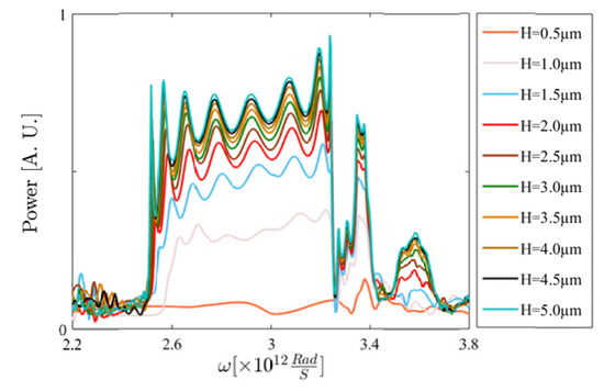
Figure 2.
Power spectra of PhC waveguides with different pillar heights (H), a latticce constant a = 245 nm and a pillar radius of r = 0.2a.
3. Hybrid Photonic Crystal Surface Plasmon Polariton System
In order to address the above-mentioned problem, in this study we propose a hybrid system comprising of finite 2D PhC pillars combined with a platform to support surface plasmon polaritons, like a thin layer of a noble metal such as gold. In this system, the lateral confinement is defined by the PhC pillars, while the vertical confinement is ruled by SPPs.
The SPPs have a high affinity to the metal surface and almost exponentially decay in the direction perpendicular to the surface. This property of SPPs has led us to c me up with a hybrid system as schematically shown in Figure 3: 2D PhC pillars for horizontal confinement (along the y-axis) on a substrate coated with a metal layer to support SPP and therefore provide confinement in vertical direction (along the z-axis).
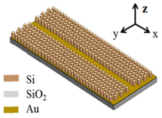
Figure 3.
Hybrid waveguide composed of Si pillars (shorter than those in Figure 1a) on SiO2 substrate and embedded in a thin layer of gold.
For the initial design, the metal layer has been excluded and the PhC has been considered to be a hexagonal lattice of Si pillars, by removing one line of the pillars a waveguide is formed as shown in Figure 1a. The dispersion diagrams of this waveguide with various pillar radii are presented in Figure 4. Frequency of the waveguide mode is in the band gap of the photonic crystal (shadowed area in Figure 1b), therefore it has laterally confined with PhC. On the other hand, it can be seen that the dispersion diagram of the waveguide modes features a fairly flat region. In order to have a low group velocity and therefore a high light-matter interaction a system design procedure is proposed with the operation frequency (wavelength) lies around the flat region of the dispersion diagram of the PhC [8].
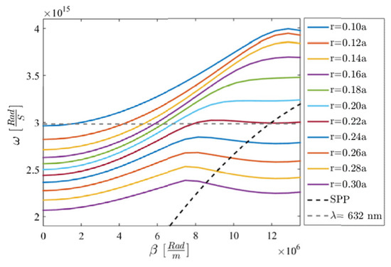
Figure 4.
Dispersion diagrams of waveguides obtained by removing one r w of pillars in 2D hexagonal PhC. The radius of Si pillars are varied from r = 0.1a to r = 0.3a. The dashed black graph shows the dispersion diagram of the SPP mode of a 40-nm gold film sandwiched between air and glass substrate. The grey dotted line represents the frequency corresponding to λ = 632 nm.
The waveguide should then be combined with an SPP system composed of a h = 40 nm gold film sandwiched between air and a glass substrate. The dispersion diagram of this triple system can be extracted from the following set of equations [1]:
In these equations, the subscripts i = 1, 2, 3 stand for air, metal and glass media, respectively. In addition, β, k0, εi and ki represent the propagation vector, the wave vector of the free space, the permittivity of each medium and the component of the wave vector perpendicular to the interface. The dispersion of β of this system is shown in Figure 4 using a black dashed line. This line intersects the dispersion diagram of the PhC waveguide with r = 0.22a at its flat region, at the frequency of our interest corresponding to λ = 632 nm (grey dashed line).
A system of a PhC waveguide (with a finite height) and the SPP layer has a dispersion property being distinct from those of the two systems and as can be seen in Figure 5a, it has the property of a split anti-crossing mode of the two original systems. With the obtained dimensions, the final hybrid system is analyzed with a height of pillars being 400 nm, which offers an aspect ratio of around 4. Figure 5b shows the mode profile of the system, where, although the height of the pillars (400 nm) is smaller than a wavelength, the mode is very well confined in the guiding region. This profile supports the strong and well-controlled propagating mode in the proposed structure.
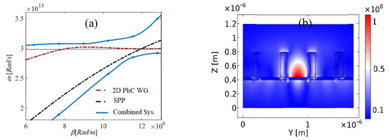
Figure 5.
(a) Dispersion diagram of a 22D PhC waveguide with r/a = 0.22 and the SPP modes of the tri-layer (shown in Figure 4) together with the dispersion diagram of the combined system (shown in Figure 3). In the combined system, the height of the pillars is just 400 nm, which is compatible MEME technology. (b) The mode profile of the hybrid system.
4. Conclusions
In this work, a hybrid system of finite 2D PhC waveguide with a plasmonic substrate is proposed and investigated. The design procedure in order to satisfy two requirements are discussed: (1) the operation frequency lies around the flat region of the dispersion diagram of the PhC waveguide in order to have a low group velocity, and (2) this point coincides with the dispersion diagram of a metallic layer sandwiched between air and the substrate. It has been shown that with this approach, the mode confinement in the vertical dimension is provided by SPP and therefore, the PhC pillars height can be decreased by a factor of 7.5, resulting in an aspect ratio of 4 which is feasible to realize in industrial fabrication. The pillar’s height can be further decreased if the guiding width (i.e., the distance between the two PhC media) is decreased. However, in this work, we did not decrease the guiding width since this yields also an increase in the effective refractive index of the guiding mode and therefore waveguide excitation becomes more difficult. In addition, we considered a working frequency in the visible spectrum. However, with a proper choice of plasmonic material, the method can be used for the design of such a system in near- and mid-infrared regime, especially for the applications in the gas sensing.
Author Contributions
R.J. and B.A. developed the concept, performed the computations. R.J., B.A. and B.J. wrote the manuscript, T.G. dealt with technological aspects, B.J. supervised the project.
Acknowledgments
The authors acknowledge the support of the “LCM—K2 Center for Symbiotic Mechatronics” within the framework of the Austrian COMET-K2 program and the COMET K1 center Austrian Smart Systems Integration Research (ASSIC).
Conflicts of Interest
Authors declare no conflict of interest.
References
- Maier, S.A. Plasmonics: Fundamentals and Applications; Springer: Bath, UK, 2006. [Google Scholar]
- Joannopoulos, J.D.; Johnson, S.G.; Winn, J.N.; Meade, R.D. Photonic Crystal Molding Flow of Light; Princeton University Press: Princeton, NJ, USA, 2008. [Google Scholar]
- Song, B.S.; Noda, S.; Asano, T.; Akahane, Y. Ultra-high-Q photonic double-heterostructure nanocavity. Nat. Mater. 2005, 4, 207–210. [Google Scholar] [CrossRef]
- Pedersen, J.; Xiao, S.; Mortensen, N.A. Slow-light enhanced absorption for bio-chemical sensing applications: Potential of low-contrast lossy materials. J. Eur. Opt. Soc. 2008, 3. [Google Scholar] [CrossRef]
- Jannesari, R.; Ranacher, C.; Consani, C.; Grille, T.; Jakoby, B. Sensitivity optimization of a photonic crystal ring resonator for gas sensing applications. Sens. Actuators A Phys. 2017, 264, 347–351. [Google Scholar] [CrossRef]
- Kraeh, C.; Martinez-Hurtado, J.L.; Zeitlmair, M.; Popescu, A.; Hedler, H.; Finley, J.J. Strong transmittance above the light line in mid-infrared two-dimensional photonic crystals. J. Appl. Phys. 2015, 117, 223101. [Google Scholar] [CrossRef]
- Jannesari, R.; Ranacher, C.; Consani, C.; Lavchiev, V.; Grille, T.; Jakoby, B. High-Quality-Factor Photonic Crystal Ring Resonator with Applications for Gas Sensing. Procedia Eng. 2016, 168, 375–379. [Google Scholar] [CrossRef]
- Mortensen, N.A.; Xiao, S. Slow-light enhancement of Beer-Lambert-Bouguer absorption. Appl. Phys. Lett. 2007, 90, 2–5. [Google Scholar] [CrossRef]
Publisher’s Note: MDPI stays neutral with regard to jurisdictional claims in published maps and institutional affiliations. |
© 2018 by the authors. Licensee MDPI, Basel, Switzerland. This article is an open access article distributed under the terms and conditions of the Creative Commons Attribution (CC BY) license (https://creativecommons.org/licenses/by/4.0/).