MEMS Enabled Bendable and Stretchable Silicon Circuits †

Abstract
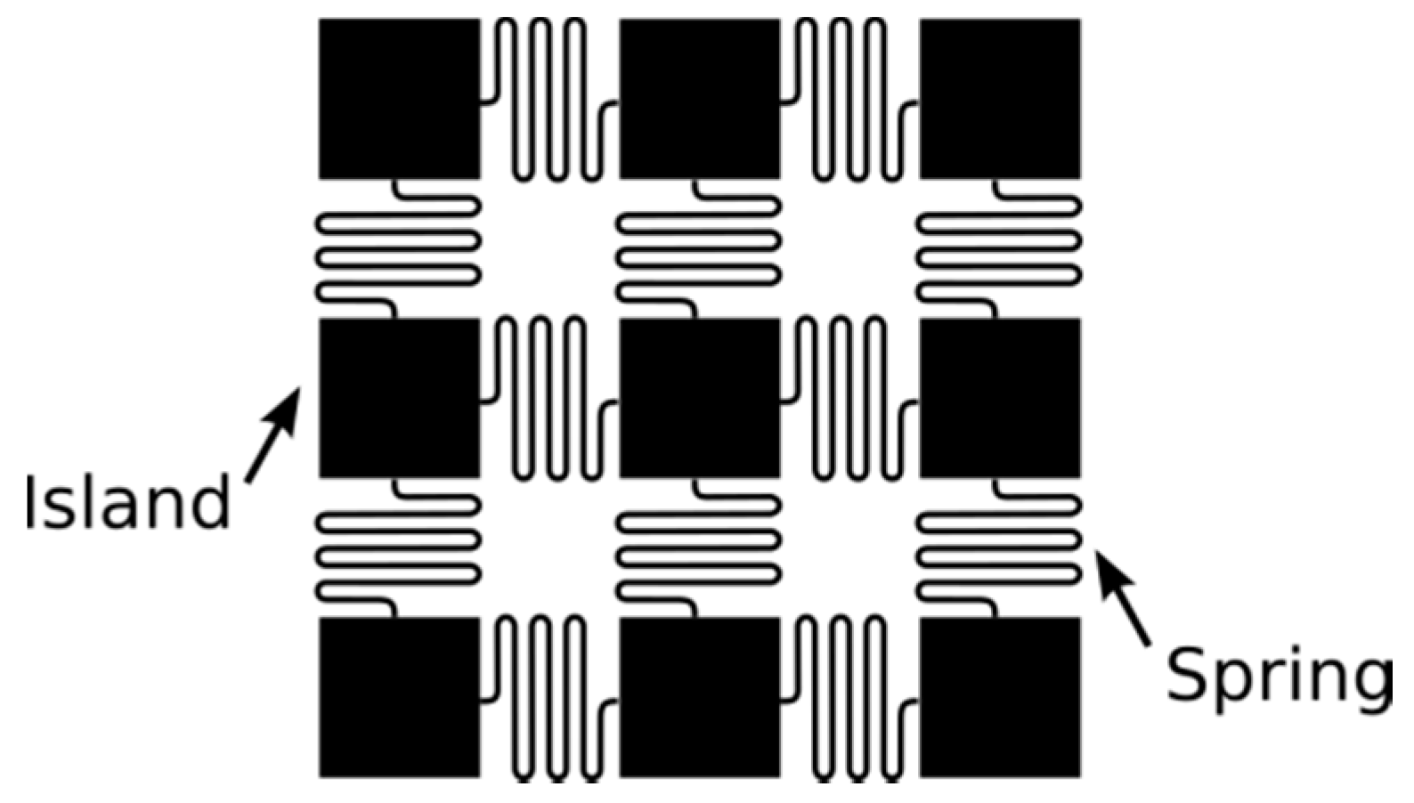
:1. Introduction
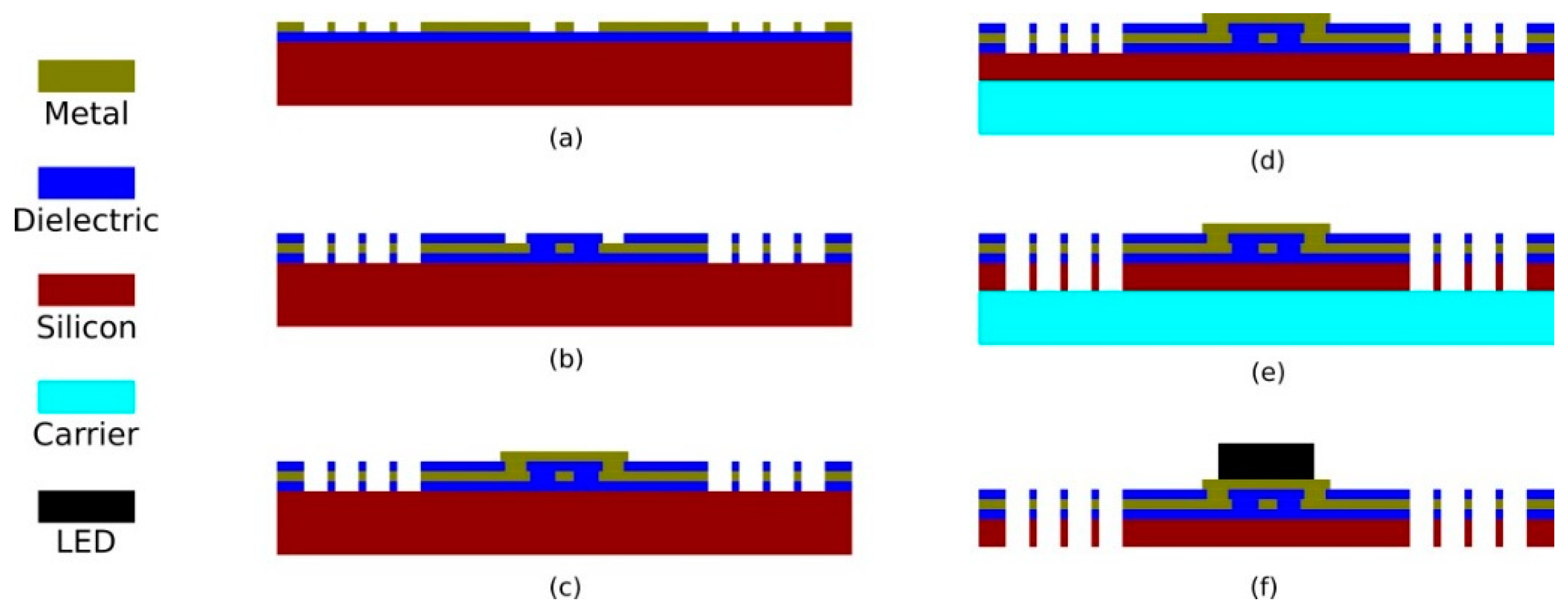
2. Materials and Methods
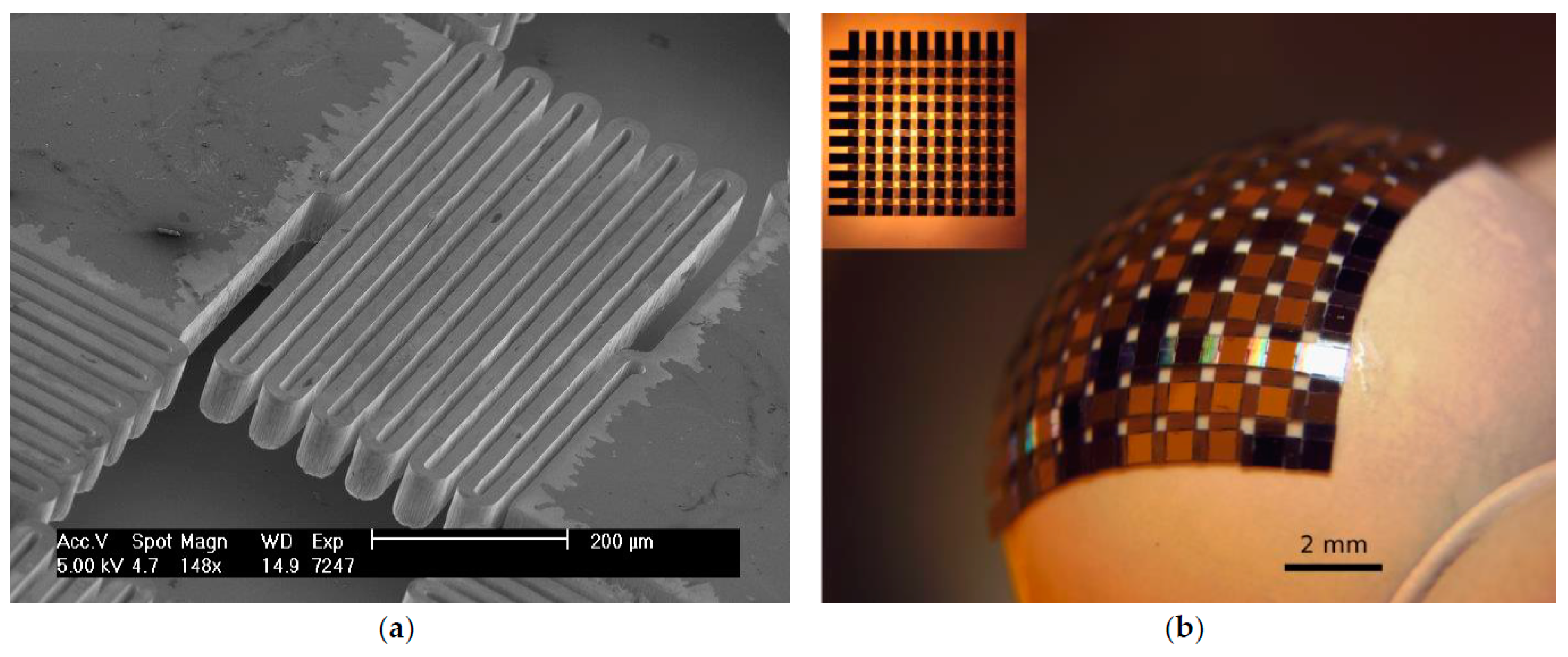
3. Results and Discussion
4. Conclusions
Funding
Conflicts of Interest
References
- Park, J.S.; Chae, H.; Chung, H.K.; Lee, S.I. Thin film encapsulation for flexible AM-OLED: A review. Semicond. Sci. Technol. 2011, 26, 034001. [Google Scholar] [CrossRef]
- Oliveira Hansen, R.M.; Liu, Y.; Madsen, M.; Rubahn, H.G. Flexible organic solar cells including efficiency enhancing grating structures. Nanotechnology 2013, 24, 145301. [Google Scholar] [CrossRef] [PubMed]
- Yoon, S.M.; Yang, S.; Byun, C.W.; Jung, S.W.; Ryu, M.K.; Park, S.H.K.; Kim, B.; Oh, H.; Hwang, C.-S.; Yu, B.G. Nonvolatile memory thin-film transistors using an organic ferroelectric gate insulator and an oxide semiconducting channel. Semicond. Sci. Technol. 2011, 26, 034007. [Google Scholar] [CrossRef]
- Dinyari, R.; Rim, S.B.; Huang, K.; Catrysse, P.B.; Peumans, P. Curving monolithic silicon for nonplanar focal plane array applications. Appl. Phys. Lett. 2008, 92, 091114. [Google Scholar] [CrossRef]
- Kim, G.; Kim, B.; Brugger, J. All-photoplatic microstencil with self-alignment for multiple layer shadowmask patterning. Sens. Actuat. A-Phys. 2003, 107, 132–136. [Google Scholar] [CrossRef]
- Lips, B.; Puers, R. Three step deep reactive ion etch for high density trench etching. J. Phys. Conf. Ser. 2016, 757, 012005. [Google Scholar] [CrossRef]

Publisher’s Note: MDPI stays neutral with regard to jurisdictional claims in published maps and institutional affiliations. |
© 2018 by the authors. Licensee MDPI, Basel, Switzerland. This article is an open access article distributed under the terms and conditions of the Creative Commons Attribution (CC BY) license (https://creativecommons.org/licenses/by/4.0/).
Share and Cite
Lips, B.; Puers, R. MEMS Enabled Bendable and Stretchable Silicon Circuits. Proceedings 2018, 2, 837. https://doi.org/10.3390/proceedings2130837
Lips B, Puers R. MEMS Enabled Bendable and Stretchable Silicon Circuits. Proceedings. 2018; 2(13):837. https://doi.org/10.3390/proceedings2130837
Chicago/Turabian StyleLips, Bram, and Robert Puers. 2018. "MEMS Enabled Bendable and Stretchable Silicon Circuits" Proceedings 2, no. 13: 837. https://doi.org/10.3390/proceedings2130837
APA StyleLips, B., & Puers, R. (2018). MEMS Enabled Bendable and Stretchable Silicon Circuits. Proceedings, 2(13), 837. https://doi.org/10.3390/proceedings2130837