Abstract
Self-heating operation, or the use of the resistance-probing signal to warm up and control the temperature of nanowire devices, has been the subject of research for more than a decade. The state-of-the-art shows that this approach is serving to lower the power demand in temperature-activated devices, especially in conductometric gas sensors, but the simplicity of eliminating the heating element comes with the complexity of integrating 1-dimensional nanomaterials in electronic devices. The advantages of the efficient self-heating effect in nanowires have already been probed in a broad range of systems and materials. But when it comes to transfer this operating principle to new systems and materials natural doubts arise: how to do it?, how much savings in power will be achieved? We will address these questions in this review contribution.
1. Introduction
Controlling the operating conditions of a sensor is crucial to obtain accurate, repeatable, and long-term stable readings. Otherwise, factors like vibration, ambient light, or temperature can interfere with the sensor signal, leading to readings not related to the magnitude being monitored. To prevent this cross-talk interference, many sensor technologies integrate some kind of actuator, either mechanical, optical or thermal. This is, in most of the cases, the main power hungry part of the device [1].
Concerning temperature control, it is mostly based on electrical resistors (for heating) and thermoelectric elements (for heating and cooling). The optimization of their power budget has usually relayed on more miniaturization (to reduce the thermal masses to be heated up [2,3]), and on better thermal isolation (to minimize the thermal losses related to heat conduction through solid parts [4,5,6]). This trend already started in the first generation of sensors with active areas at a millimeter scale [7], which was later reduced to tens-to-hundreds of microns with the use of microfabrication techniques (MEMS) [3,5,8,9,10,11]. Today, with the advent of nanotechnology (NEMS), we are approaching to the sub-micron regime [12,13]. In fact, nanotechnology enables the use of a nanowire-based heating method with potential for ultra-low power consumption, the self-heating effect, which is the subject reviewed in the following pages.
The advantages of the efficient self-heating effect in nanowires have already been probed in a broad range of systems and materials. But when it comes to transfer this operating principle to new systems and materials natural doubts arise: how to do it?, to what extend the desired features will be achieved?
This paper aims at providing general guidelines for the achievement of efficient self-heating in new materials and system configurations. These suggestions are built upon knowledge available in a broad literature, the own experience of the authors, and finite elements simulations (FEM) carried out specifically to clarify some grey points. To that end, we used the COMSOL Multiphysics software to perform the modeling with the Joule Heating module [14].
For the sake of simplicity, only an individual suspended nanowire has been considered. The electrical access was made through two gold pads on top of a silicon bulk with a SiO2 insulator layer (Figure 1). Simulation parameters, such as electrical conductivity, thermal conductivity and nanowire dimensions, were selected in a broad range of values, considering most of the materials used in the literature for sensing devices [15,16,17,18,19,20,21,22,23,24]. In all cases, a convective cooling boundary condition with a heat transfer of h = 5 W·m−2·K−1 has been applied.
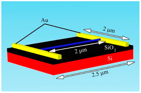
Figure 1.
3D scheme of the single-wire model between to metal contacts used for FEM simulations. Reproduced from Ref. [40], with permission from Elsevier.
2. Materials Shape and Dimensions
As described in the previous section, there are many reports on devices taking advantage of the self-heating effect in nanostructured materials. Today, it is out of question that relatively efficient self-heating can be achieved in typical semiconductor materials (e.g., Si, Ge, GaN), metal oxides (SnO2, ZnO, TiO2, In2O3), carbon allotropes (CNT, CNF, graphene, etc.) if they are shrunk down to the nanoscale in some of their dimensions.
The need for providing a clear and thin path for the current flowing from end to end, along the heated material, suggests a certain preference for 1D (i.e., nanowire, nanotube) or 2D (e.g., graphene) nanostrucutres. In fact, no efficient self-heating effects have been reported for 3D nanoparticles, which typically form aggregates offering thicker current paths.
Concerning sizes, efficient self-heating usually emerges from nanoparticles with characteristic confinement dimensions well below 100 nm. However, as shown in the following sections, this number is strongly dependent on the transport properties of the materials. Still, there is a general trend that suggest that, for the same material and in the same device configuration, the thinner the nanostructure, the higher the heating efficiency (Figure 2). According to our simulations, the increment of the temperature is inversely proportional to the cross-section of the 1D nanostructure being heated. In the case of a cylindric nanowire, this relationship can be written as
where rnw is the radius of the nanowire, or in a more general 1D material, any characteristic dimension of the transversal confinement.
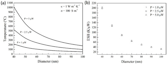
Figure 2.
(a) Temperature reached at the center of the nanowire model, and (b) efficient self-heating coefficient (ESH) as a function of the nanowire diameter and the dissipated power with constant thermal and electrical conductivities. Reproduced from Ref. [40], with permission from Elsevier.
3. Electrical Transport Properties
The fact of measuring the efficiency of the self-heating effect in terms of the electrical power needed to achieve a certain temperature usually leads to the misconception that the efficiency of this heating phenomena is closely related to the electrical transport properties of the materials used (e.g., electrical conductivity). This is, however, not the case.
To illustrate this question we carried out FEM simulations of the self-heating effect in one single nanowire of 2 μm in length and 60 nm in diameter bridging between two Au electrodes, considering different electrical conductivities, from σ = 1 S·m-1 to σ = 104 S·m-1 and a constant thermal conductivity of κ = 1 W·m−1·K−1. This range of σ variation corresponds to typical values of relevant materials, from SnO2 to carbon nanofibers, in a nanostructured form, which is usually higher than their bulk counterparts [15,16,17,18,19]. Figure 3a clearly shows that, independently on the electrical conductivity, nearly identical temperatures are achieved for the same power consumption (i.e., the same ESH).
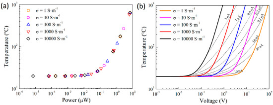
Figure 3.
Temperatures reached at the center of the nanowire with different electrical conductivities as a function of (a) the power dissipated, and (b) the voltage applied to a nanowire diameter of 60 nm and a thermal conductivity of κ = 1 W·m−1·K−1. Reproduced from Ref. [40], with permission from Elsevier.
However, the electrical transport properties have a major impact on the convenience and practicability of implementing a self-heated device. The electrical conductance determines how the electrical power required for heating must be applied. As illustrated in Figure 3b, large conductivities involve lower voltages and higher currents. Conversely, low conductivities require lower current levels at a much higher voltage. From the point of view of convenience, the first case might be simpler to implement with conventional electronic components, typically designed for operation in the range of a few volts. Also, the need of higher voltage levels may lead to additional energy losses (e.g., due to the voltage boosting), detrimental for a low power operation mode. Of course, there are also limits on the amount of current that low power devices could provide, but this aspect is usually easier to circumvent with a proper electronic design.
Again, no universal rule seems to exist but, in the authors’ experience, electrical resistances in the range of thousands of ohm provide a good balance in terms of convenience for operation. Beware that this rule of thumbs relates to the macroscopic resistance, which involves not only the conductivity of the material but also its geometrical arrangement. This means that given a material, its final electrical behavior can be adjusted, to some extent by tailoring the device geometry.
4. Heat Transport Properties
Contrary to the case of electric transport, the properties related to heat transport play a crucial role in the effectiveness of the heating.
Specific simulations, in which the thermal conductivity κ of a nanowire with σ = 100 S·m−1 was swept from 10-2 to 102 W·m−1·K−1 [20,21,22,23,24] showed that the decrease in κ leads to smaller amounts of electrical power needed to reach the same temperature (Figure 4).
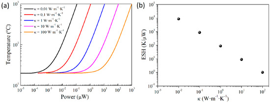
Figure 4.
(a) Temperature reached at the center of the nanowire as function of the power dissipated with different thermal conductivities and (b) efficient self-heating coefficient (ESH) as a function of the thermal conductivity with a nanowire diameter of 60 nm and a electrical conductivity of σ = 100 S·m−1. Reproduced from Ref. [40], with permission from Elsevier.
In conventional bulk materials, modifying the thermal conductivity is complex. In contrast, big modifications are relatively simple in nanomaterials, due to the strong influence on the phonon scattering properties of confinement and shape. For example, bulk SnO2 has a thermal conductivity in the range of 50–100 W·m−1·K−1 [20], while its nanometric counterpart can be one or two orders of magnitude lower, 1–5 W·m−1·K−1 [21].
Thus, the modification of the thermal conductivity offers a path for further research in the optimization of heat and electron transport, with the aim of a more efficient heating.
5. Thermal Loses With the Substrate
In addition to the transport of energy trough the materials under Joule heating, the losses of thermal energy play a fundamental role in the discussion of efficient heating achievement.
The early works exploring the effects of Joule heating in thin films (reporting moderate heating with large amounts of power dissipated) suggested [25] and the more recent works, (exploring the possibility of shrinking the conduction path of a thin film in a top-down attempt to build up an energy efficient wire) confirmed [26] that the thermal losses by conduction with the substrate and/or the contacts are the major threat for the self-heating efficiency. To circumvent this problem and optimize the heating efficiency, some authors chose to separate the material from the substrate in suspended configurations [12]. This approach proved to be successfully reaching record power efficiency figures despite the complexity. However, there are also many works showing nanowire-like structures lying apparently in direct contact with a substrate that report efficient heating.
To better understand this issue, we carried out again specific FEM simulations adjusting the degree of contact between one single nanowire in self-heating operation and a flat substrate. Detailed studies of the thermal transfer mechanism at the nanoscale [27,28], not only with the substrate but also with the ambience [29], contacts [30,31], etc. are found elsewhere.
Figure 5 shows the thermal behavior in the case of (a) full flat contact, (b and c) discontinuous contact, and (d) no contact (i.e., suspended wire). In all cases, the same amount of power was dissipated in the wire. Clearly, in accordance with the qualitative trends observed in the experiments, a full an intimate contact between the wire and the substrate hampers all sort of efficient heating. On the other hand, fully suspended nanostructures, even at distances from the substrate as small as 1 nm, show the best results in terms of heating efficiency, as expected from many of the experiments reported elsewhere. Interestingly, the intermediate situations also lead to significant, but lower, temperature increases for the same amount of power (ESH ~ 47, 68 and 88 for the simulations in Figure 5b–d, respectively). This last result suggests that, possibly, the contact with the substrate is not complete in devices based on nanowires laying on a substrate. It is plausible thinking that, at such small scale, minor effects like surface roughness, wire bending, etc. easily lead to a discontinued contact scenario.
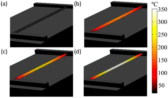
Figure 5.
3D model of the simulated temperature profile along a nanowire with d = 60 nm, σ = 100 S·m−1 and κ = 1 W·m−1·K−1 in four different scenarios: (a) full flat contact with the substrate; (b) with 10 contact points; (c) with 5 contact points; and (d) fully suspended. A power of 3.7 μW was applied in all cases. Reproduced from Ref. [40], with permission from Elsevier.
6. Multiple Nanowires
As mentioned above, efficient self-heating can also be achieved in systems containing multiple nanowires. Apparently, a network of 1D wires forms a thermal insulating scaffold structure that prevents the direct contact between the substrate and most of the material. This way, the spots in the network that combining sufficient insulation with proper electrical connectivity concentrate most of the heating (Figure 6a) [32,33,34,35,36,37,38,39]. To illustrate this phenomenon, a structure made of multiple nanowires randomly interconnected has been simulated (Figure 6b). Clearly, the nanowire portions in direct contact with the substrate reach temperatures well below the ones achieved in the upper nanowire parts. For the sake of comparison, the efficiency of this structure was ESH ~ 32, in contrast with the ESH ~ 88 found for a single nanowire (Figure 6d). Despite this three-fold reduction of the efficiency, the approach is much simpler to implement and still allows for very low power operation. The questions of how these efficiencies scale with the number of wires in the network and how the network size average out the differences between different random arrangements in different devices are still unanswered, but are crucial to elucidate the future of this approach.
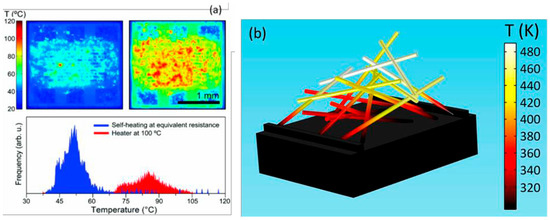
Figure 6.
(a) Experimental observations (thermal micrographs) of hot-spots in random networks of CNF operated (left) in self-heating mode and (right) with an external heater. Clearly, the temperature pattern in self-heating mode concentrates in some central regions of the nanowire network. This is also seen as disperse high-temperature spikes in the blue histogram of the micrographs above, corresponding to the self-heating operation. Reproduced from Ref. [38] with permission from the Royal Society of Chemistry. (b) 3D model of the simulated temperature profile in a random network of nanowires (d = 60 nm, σ = 100 S·m−1, and κ = 1 W·m−1·K−1) operated at 6.8 μW. The nanowire portions in direct contact with the substrate remain cooler than those located further away from the substrate. Reproduced from Ref. [40], with permission from Elsevier.
7. Recommendations for an Efficient Self-Heating
From the previous considerations (dimensions, electrical and heat transport properties, and thermal losses), the following conclusions can be drawn:
- i.
- For obvious reasons, the cross-section dimensions of the wires are crucial, as the temperature is inversely proportional to the square of the characteristic width of the nanoparticle (e.g., radius in the case of a cylindrical nanowire).
- ii.
- In terms of materials properties, thermal conductivity is the determining factor for an efficient self-heating. Confinement effects at the nanoscale can modify the thermal conductivity in the direction of improving the efficiency.
- iii.
- The electrical properties (i.e., electrical conductivity or resistivity) are not the key factors to achieve efficient self-heating, but they are accountable for the conditions in which the electrical power should be applied.
- iv.
- Thermal loses with all elements in contact with the self-heated material (usually, substrate and electrical contacts) are greatly detrimental for the efficiency. While some thermal insulation is needed, just a few nanometers might be enough to dramatically reduce these thermal losses.
- v.
- Multiple-wire configuration may help to create the suitable thermal insulation conditions, facilitating device integration, but opening new challenges in device reproducibility.
- vi.
- The coupling between sensing effects and temperature effects on the nanowire resistance affects the amount of power being dissipated. This effect does not compromise the ability to increase the temperature of the material, but limits the accuracy in controlling the actual temperature reached in self-heating mode.
8. Conclusions
In this work, we have reviewed the progress made to date in nanowire devices operated with self-heating. It is proposed an objective parameter to quantify and compare the efficiencies achieved in different devices and configurations: the Efficient Self-Heating coefficient. Finally, we compile a set of recommendations (based on own experience, literature, and finite-element simulations) to guide the design of future devices of this kind.
After a decade of research, the potential of this approach for lowering the power consumption in temperature-activated sensors has been undoubtfully demonstrated. The future of the approach hangs on our ability to overcome the challenges of integrating one single 1D nanoparticle in an electronic device, or on our ingenuity to recover the same low-power features in much simpler configurations.
Author Contributions
J.D.P., C.F. and O.C. conceived and wrote the paper. C.F. performed and analized the simulations.
Acknowledgments
The research leading to these results has received funding from the European Research Council under the European Union’s Seventh Framework Program (FP/2007-2013)/ERC Grant Agreement n. 336917. J.D. Prades acknowledges the support from the Serra Húnter Program.
References
- de Silva, C.W. Sensors and Actuators: Engineering System Instrumentation, 2nd ed.; CRC Press: Boca Raton, FL, USA, 2015. [Google Scholar]
- Semancik, S.; Cavicchi, R. Kinetically Controlled Chemical Sensing Using Micromachined Structures. Acc. Chem. Res. 1998, 31, 279–287. [Google Scholar] [CrossRef]
- Semancik, S.; Cavicchi, R.E.; Wheeler, M.C.; Tiffany, J.E.; Poirier, G.E.; Walton, R.M.; Suehle, J.S.; Panchapakesan, B.; DeVoe, D.L. Microhotplate platforms for chemical sensor research. Sens. Actuators B Chem. 2001, 77, 579–591. [Google Scholar] [CrossRef]
- Graf, M.; Barrettino, D.; Baltes, H.P.; Hierlemann, A. CMOS Hotplate Chemical Microsensors; Springer-Verlag: Berlin, Germany, 2007. [Google Scholar]
- Elmi, I.; Zampolli, S.; Cozzani, E.; Mancarella, F.; Cardinali, G.C. Development of ultra-low-power consumption MOX sensors with ppb-level VOC detection capabilities for emerging applications. Sens. Actuators B Chem. 2008, 135, 342–351. [Google Scholar] [CrossRef]
- Giberti, A.; Guidi, V.; Vincenzi, D. A study of heat distribution and dissipation in a micromachined chemoresistive gas sensor. Sens. Actuators B Chem. 2011, 153, 409–414. [Google Scholar] [CrossRef]
- Taguchi, N. Gas-Detecting Device. U.S. Patent 3,631,436, 1971. [Google Scholar]
- Briand, D.; Krauss, A.; Van der Schoot, B.; Weimar, U.; Barsan, N.; Göpel, W.; De Rooij, N.F. Design and fabrication of high-temperature micro-hotplates for drop-coated gas sensors. Sens. Actuators B Chem. 2000, 68, 223–233. [Google Scholar] [CrossRef]
- Puigcorbé, J.; Vogel, D.; Michel, B.; Vila, A.; Gracia, I.; Cane, C.; Morante, J.R. Thermal and mechanical analysis of micromachined gas sensors. J. Micromech. Microeng. 2003, 13, 548–556. [Google Scholar] [CrossRef]
- Iwaki, T.; Covington, J.A.; Gardner, J.W.; Udrea, F.; Blackman, C.S.; Parkin, I.P. SQI-CMOS heaters for gas sensors. IEEE Sens. 2006, 1–3, 460–463. [Google Scholar]
- Vallejos, S.; Grácia, I.; Chmela, O.; Figueras, E.; Hubálek, J.; Cané, C. Chemoresistive micromachined gas sensors based on functionalized metal oxide nanowires: Performance and reliability. Sens. Actuators B. Chem. 2016, 235, 525–534. [Google Scholar] [CrossRef]
- Chikkadi, K.; Muoth, M.; Maiwald, V.; Roman, C.; Hierold, C. Ultra-low power operation of self-heated, suspended carbon nanotube gas sensors. Appl. Phys. Lett. 2013, 103, 223109. [Google Scholar] [CrossRef]
- Kim, Y.D.; Kim, H.; Cho, Y.; Ryoo, J.H.; Park, C.H.; Kim, P.; Kim, Y.S.; Lee, S.; Li, Y.; Park, S.N.; Yoo, Y.S. Bright visible light emission from grapheme. Nat. Nanotechnol. 2015, 10, 1–7. [Google Scholar] [CrossRef]
- COMSOL AB COMSOL Multiphysics® v. 5.2. 2017. Available online: https://www.comsol.com/ (accessed on 1 December 2018).
- Earle, M.D. The electrical conductivity of titanium dioxide. Phys. Rev. 1942, 61, 56–62. [Google Scholar] [CrossRef]
- Comini, E.; Guidi, V.; Malagu, C.; Martinelli, G.; Pan, Z.; Sberveglieri, G.; Wang, Z.L. Electrical Properties of Tin Dioxide Two-Dimensional Nanostructures. J. Phys. Chem. B 2004, 108, 1882–1887. [Google Scholar] [CrossRef]
- Sakurai, M.; Wang, Y.G.; Uemura, T.; Aono, M. Electrical properties of individual ZnO nanowires. Nanotechnology 2009, 20, 155203. [Google Scholar] [CrossRef]
- Fàbrega, C.; Hernández-Ramírez, F.; Prades, J.D.; Jiménez-Díaz, R.; Andreu, T.; Morante, J.R. On the photoconduction properties of low resistivity TiO2 nanotubes. Nanotechnology 2010, 21, 445703. [Google Scholar] [CrossRef]
- Žagar, K.; Fàbrega, C.; Hernandez-Ramirez, F.; Prades, J.D.; Morante, J.R.; Rečnik, A.; Čeh, M. Insight into the structural, electrical and photoresponse properties of individual Fe: SrTiO3 nanotubes. Mater. Chem. Phys. 2013, 141, 9–13. [Google Scholar] [CrossRef]
- Turkes, P.; Pluntke, C.; Helbig, R. Thermal conductivity of SnO2 single crystals. J. Phys. C Solid State Phys. 1980, 13, 4941–4951. [Google Scholar] [CrossRef]
- Shi, L.; Hao, Q.; Yu, C.; Mingo, N.; Kong, X.; Wang, Z.L. Thermal conductivities of individual tin dioxide nanobelts. Appl. Phys. Lett. 2004, 84, 2638–2640. [Google Scholar] [CrossRef]
- Özgür, Ü.; Gu, X.; Chevtchenko, S.; Spradlin, J.; Cho, S.J.; Morkoc, H.; Pollak, F.H.; Everitt, H.O.; Nemeth, B.; Nause, J.E. Thermal conductivity of bulk ZnO after different thermal treatments. J. Electron. Mater. 2006, 35, 550–555. [Google Scholar] [CrossRef]
- Im, J.S.; Kim, S.J.; Kang, P.H.; Lee, Y.S. The improved electrical conductivity of carbon nanofibers by fluorinated MWCNTs. J. Ind. Eng. Chem. 2009, 15, 699–702. [Google Scholar] [CrossRef]
- Mahanta, N.K.; Abramson, A.R.; Lake, M.L.; Burton, D.J.; Chang, J.C.; Mayer, H.K.; Ravine, J.L. Thermal conductivity of carbon nanofiber mats. Carbon 2010, 48, 4457–4465. [Google Scholar] [CrossRef]
- Salehi, A. A highly sensitive self heated SnO2 carbon monoxide sensor. Sens. Actuators B Chem. 2003, 96, 88–93. [Google Scholar] [CrossRef]
- Afshar, M.; Preiß, E.M.; Sauerwald, T.; Rodner, M.; Feili, D.; Straub, M.; König, K.; Schütze, A.; Seidel, H. Indium-tin-oxide single-nanowire gas sensor fabricated via laser writing and subsequent etching. Sens. Actuators B Chem. 2015, 215, 525–535. [Google Scholar] [CrossRef]
- Vasileska, D.; Raleva, K.; Hossain, A.; Goodnick, S.M. Current progress in modeling self-heating effects in FD SOI devices and nanowire transistors. J. Comput. Electron. 2012, 11, 238–248. [Google Scholar] [CrossRef]
- Hunley, D.P.; Johnson, S.L.; Flores, R.L.; Sundararajan, A.; Strachan, D.R. Analytical model for self-heating in nanowire geometries. J. Appl. Phys. 2013, 113, 234306. [Google Scholar] [CrossRef]
- Pala, M.G.; Cresti, A. Increase of self-heating effects in nanodevices induced by surface roughness: A full-quantum study. J. Appl. Phys. 2015, 117, 084313. [Google Scholar] [CrossRef]
- Vasileska, D.; Hossain, A.; Raleva, K.; Goodnick, S.M. The role of the source and drain contacts on self-heating effect in nanowire transistors. J. Comput. Electron. 2010, 9, 180–186. [Google Scholar] [CrossRef]
- Rhyner, R.; Luisier, M. Influence of thermal losses at the gate contact of Si nanowire transistors: A phenomenological treatment in quantum transport theory. Appl. Phys. Lett. 2017, 110, 103508. [Google Scholar] [CrossRef]
- Zhu, L.F.; She, J.C.; Luo, J.Y.; Deng, S.Z.; Chen, J.; Ji, X.W.; Xu, N.S. Self-heated hydrogen gas sensors based on Pt-coated W18O49 nanowire networks with high sensitivity, good selectivity and low power consumption. Sens. Actuators B Chem. 2011, 153, 354–360. [Google Scholar] [CrossRef]
- Chinh, N.D.; van Toan, N.; van Quang, V.; van Duy, N.; Hoa, N.D.; van Hieu, N. Comparative NO2 gas-sensing performance of the self-heated individual, multiple and networked SnO2 nanowire sensors fabricated by a simple process. Sens. Actuators B Chem. 2014, 201, 7–12. [Google Scholar] [CrossRef]
- Guilera, J.; Fàbrega, C.; Casals, O.; Hernández-Ramírez, F.; Wang, S.; Mathur, S.; Udrea, F.; De Luca, A.; Ali, S.Z.; Romano-Rodríguez, A.; Prades, J.D. Facile integration of ordered nanowires in functional devices. Sens. Actuators B Chem. 2015, 221, 104–112. [Google Scholar] [CrossRef]
- Monereo, O.; Casals, O.; Prades, J.D.; Cirera, A. A Low-cost Approach to Low-power Gas Sensors Based on Self-Heating Effects in Large Arrays of Nanostructures. Procedia Eng. 2015, 120, 787–790. [Google Scholar] [CrossRef][Green Version]
- Monereo, O.; Prades, J.D.; Cirera, A. Self-heating effects in large arrangements of randomly oriented carbon nanofibers: Application to gas sensors. Sens. Actuators B Chem. 2015, 211, 489–497. [Google Scholar] [CrossRef]
- Monereo, O.; Casals, O.; Prades, J.D.; Cirera, A. Self-heating in pulsed mode for signal quality improvement: Application to carbon nanostructures-based sensors. Sens. Actuators B Chem. 2016, 226, 254–265. [Google Scholar] [CrossRef]
- Monereo, O.; Illera, S.; Varea, A.; Schmidt, M.; Sauerwald, T.; Schütze, A.; Cirera, A.; Prades, J.D. Localized self-heating in large arrays of 1D nanostructures. Nanoscale 2016, 8, 5082–5088. [Google Scholar] [CrossRef]
- Tan, H.M.; Manh Hung, C.; Ngoc, T.M.; Nguyen, H.; Duc Hoa, N.; Van Duy, N.; Hieu, N.V. Novel Self-Heated Gas Sensors Using on-Chip Networked Nanowires with Ultralow Power Consumption. ACS Appl. Mater. Interfaces 2017, 9, 6153–6162. [Google Scholar] [CrossRef]
- Fàbrega, C.; Casals, O.; Hernández-Ramírez, F.; Prades, J.D. A review on efficient self-heating in nanowire sensors: Prospects for very-low devices. Sens. Actuators B Chem. 2018, 256, 797–811. [Google Scholar] [CrossRef]


Publisher’s Note: MDPI stays neutral with regard to jurisdictional claims in published maps and institutional affiliations. |
© 2018 by the authors. Licensee MDPI, Basel, Switzerland. This article is an open access article distributed under the terms and conditions of the Creative Commons Attribution (CC BY) license (https://creativecommons.org/licenses/by/4.0/).