1. Introduction
Porous silicon (pSi) is a well-studied material providing various application scenarios such as optical rugate mirrors [
1], super-capacitors [
2] or as sacrificial material in MEMS engineering [
3]. Without a doubt, pSi is a promising material in many fields of research and industry but it is not stable when it comes to application scenarios in harsh environments such as high temperatures [
4] or alkaline electrolyte solutions [
3]. In such cases porous silicon carbide (pSiC) could replace pSi. Most recently, metal assisted photochemical etching of 4H-SiC wafers has been shown to be a reliable method for forming pSiC [
5]. In particular with this method it is also possible to create a line of breakage underneath a highly porous SiC layer. Such structures with an under-etched porous layer can be locally defined. These achievements are the basis for the controlled separation of compressively stressed thin films from the substrate, leading to buckled membranes. Such membranes might show potential application in microfluidics as well as in actuators for studying the response of biological cells to mechanic stimuli [
6]. In this study, buckled membranes were fabricated on 4H-SiC wafers by depositing amorphous SiC (a-SiC:H) onto locally defined, square shaped, porosified areas. Since only chemically inert SiC was used the presented membranes are ideal candidates for the before mentioned application scenarios.
2. Materials and Methods
Metal assisted photochemical etching (MAPCE) has been performed onto single crystalline 4H-SiC wafers with a specific resistivity of (0.012–0.025) Ω
·cm. Therefore, 100 nm of platinum were sputter deposited onto the surface of the 4H-SiC samples acting both as anode and etching resist during MAPCE. Afterwards, the samples were immersed in an etching solution containing 0.15 mol/L H
2O
2 and 1.31 mol/L HF for 150 min. During this period of time the samples were irradiated with UV light having a wavelength of 254 nm. Finally, the Pt thin films were removed with boiling aqua regia leading to square areas of locally defined porous SiC having side lengths of 50 and 100 µm as it is reported in [
7]. The experimental and theoretical details of the applied MAPCE approach can be found in [
5].
Afterwards amorphous, hydrogenated SiC (a-SiC:H) was deposited onto the samples by utilizing a PECVD Oxford Instruments PlasmaLab 100 ICP-CVD reactor. As reactive gases methane and silane were used while the reactive gas flow ratio of methane was 0.675 at a total reactant flow of 20 sccm. The ICP coil power was set to 2000 W, no RF table power was applied and the substrate temperature was set to 250 °C. Finally, the chamber back pressure was regulated to 8 µbar at an argon flow rate of 50 sccm additionally to the reactant gases. Under these conditions 0.5 µm of a-SiC:H were deposited at a deposition rate of 13.6 nm/min. The resulting compressive thin film stress was −770 MPa.
For measuring the deflection of a buckled membrane a Polytec MSA-400 white light interferometer operated in in phase-shift mode was used. For image generation a scanning electron microscope (Hitachi SU8030) using acceleration voltages between 2 and 5 kV was used.
3. Results and Discussion
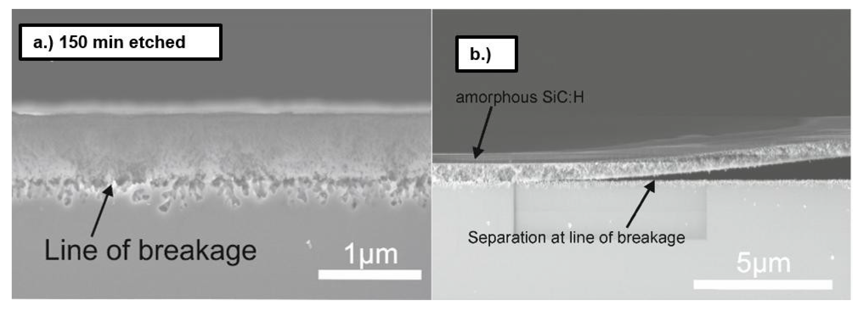
Figure 1a shows a highly porous layer which is under-etched by a line of breakage. Recent findings allow an interpretation of this phenomenon [
5].
During MAPCE the porous layer is covered with functional groups such as -CH
x or Si-O-Si. With increasing H
2O
2 concentration the density of functional groups at the surface increases as well. On the other hand UV-light irradiation is necessary during MAPCE to generate electron/hole pairs at the etching solution/electrolyte interface. The radiation provided by the UV source with a wavelength of 254 nm splits H2O2 into radicals according to Equation (1). Thus with increasing H2O2 concentration also its rate of degradation is increased. This leads to a decreased density of functional groups at the bottom of the porous layer. Since the functional groups protect the porous layer from total dissolution the upper layer is protected, while a line of breakage forms at its bottom as can be observed in
Figure 1a.
Such a highly porous layer was covered with a layer of amorphous SiC:H as is illustrated in
Figure 1b. A separation of the highly porous layer from the bulk substrate at the line of breakage can be observed. This shows that there is a greater adhesion between the deposited a-SiC:H thin film and the highly porous SiC than between the latter and the unmodified substrate. So truly a line of breakage was fabricated, but still the realization of a buckled membrane needed to be proved.
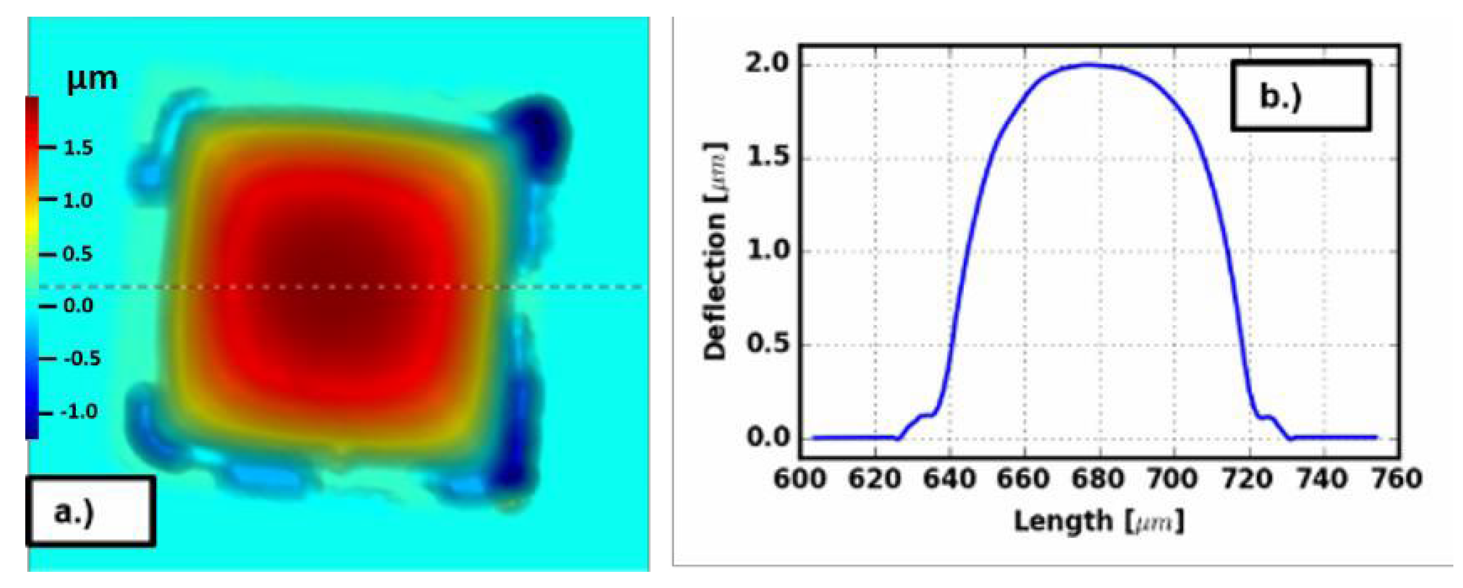
Therefore white light interferometry measurements of a square area of porous SiC after a:SiC:H deposition were performed. The results are illustrated in
Figure 2. Indeed a buckled membrane was observed as can be seen in
Figure 2a. The corresponding curve of the membrane deflection along the dotted line is shown in
Figure 2b.
4. Conclusions and Outlook
In summary it could be shown that amorphous SiC:H deposited with PECVD in combination with highly porous SiC generated with MAPCE is a suitable method for the preparation of buckled membranes.
Such membranes consist only of SiC, making them suitable for many application scenarios where chemical inertness is desired such as actuators which are used for the stimulation of biological cells.
Author Contributions
M.L., M.D. and C.Z. performed the experimental work. The interpretation of the results was done by M.L., C.Z., M.S., M.D. and U.S.
Acknowledgments
This project has been supported by the COMET K1 centre ASSIC Austrian Smart Systems Integration Research Center. The COMET—Competence Centers for Excellent Technologies—Programme is supported by BMVIT, BMWFW, and the federal provinces of Carinthia and Styria.
Conflicts of Interest
“The authors declare no conflict of interest. The founding sponsors had no role in the design of the study; in the collection, analyses, or interpretation of data; in the writing of the manuscript, and in the decision to publish the results”.
References
- Lorenzo, E.; Oton, C.J.; Capuj, N.E.; Ghulinyan, M.; Navarro-Urrios, D.; Gaburro, Z.; Pavesi, L. Porous silicon-based rugate filters. Appl. Opt. 2005, 44, 5415–5421. [Google Scholar] [CrossRef] [PubMed]
- Oakes, L.; Westover, A.; Mares, J.W.; Chatterjee, S.; Erwin, W.R.; Bardhan, R.; Weiss, S.M.; Pint, C.L. Surface engineered porous silicon for stable, high performance electrochemical supercapacitors. Sci. Rep. 2013, 3, 3020. [Google Scholar] [CrossRef] [PubMed]
- Bell, T.E.; Gennissen, P.T.J.; DeMunter, D.; Kuhl, M. Porous silicon as a sacrificial material. J. Micromech. Microeng. 1996, 6, 361. [Google Scholar] [CrossRef]
- Mawhinney, D.B.; Glass, J.A.; Yates, J.T. FTIR study of the oxidation of porous silicon. J. Phys. Chem. B 1997, 101, 1202–1206. [Google Scholar] [CrossRef]
- Leitgeb, M.; Zellner, C.; Schneider, M.; Schwab, S.; Hutter, H.; Schmid, U. Metal assisted photochemical etching of 4H silicon carbide. J. Phys. D Appl. Phys. 2017, 50, 435301. [Google Scholar] [CrossRef]
- Nguyen, T.K.; Phan, H.P.; Kamble, H.; Vadivelu, R.; Dinh, T.; Iacopi, A.; Walker, G.; Hold, L.; Nguyen, N.T.; Dao, D.V. Superior Robust Ultrathin Single-Crystalline Silicon Carbide Membrane as a Versatile Platform for Biological Applications. ACS Appl. Mater. Interfaces 2017, 9, 41641–41647. [Google Scholar] [CrossRef] [PubMed]
- Leitgeb, M.; Zellner, C.; Pfusterschmied, G.; Schneider, M.; Schmid, U. Porous Silicon Carbide for MEMS. Proceedings 2017, 1, 297. [Google Scholar] [CrossRef]
| Publisher’s Note: MDPI stays neutral with regard to jurisdictional claims in published maps and institutional affiliations. |
© 2018 by the authors. Licensee MDPI, Basel, Switzerland. This article is an open access article distributed under the terms and conditions of the Creative Commons Attribution (CC BY) license (https://creativecommons.org/licenses/by/4.0/).

