Abstract
Hybrid System-in-Foil exploits the complementary benefits of integrating embedded silicon chips with on-foil passive and active electronic components. In this work, the design, fabrication and characterization of three on-foil components, namely a humidity sensor, near field communication antenna and organic thin-film transistors, are investigated.
1. Introduction
Currently, most flexible electronic components are either fabricated as standalone components or combined with bulky sensor readout and/or wireless communication silicon chips glued to the surface of a flexible substrate [1,2,3]. Other recent designs use only one technology to achieve a true bendable sensor system, e.g., integrated temperature sensor and A/D converter using amorphous Indium-Gallium-Zinc-Oxide (InGZnO) thin-film transistors [4].
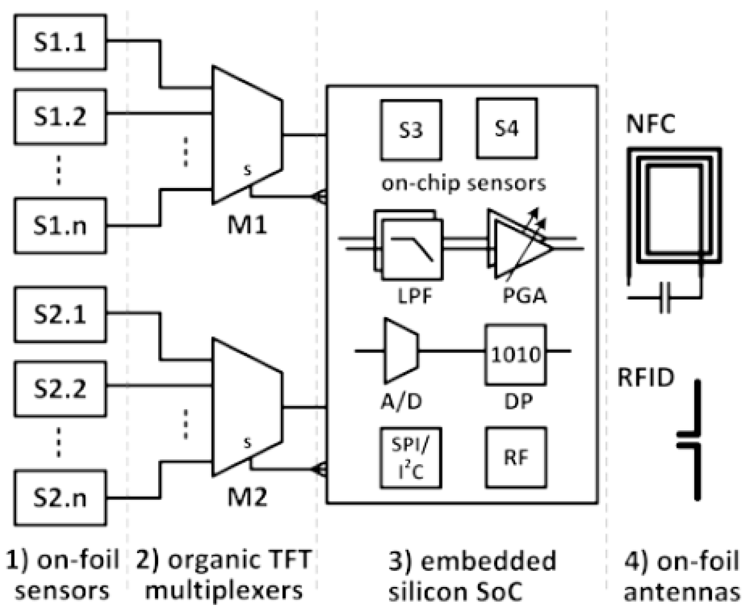
As presented in Figure 1, Hybrid System-in-Foil (HySiF) targets an economical implementation of ultra-thin sensor systems by integrating minimum number of embedded silicon chips and maximizing the number of on-foil components. Compared to prior art, HySiF combines unique characteristics such as low-power operation provided by the advanced CMOS technology, thin-form factor of the embedded Si chip (20 µm) and foil packaging (thickness ≈ 60 µm), and large area feasibility of the on-foil sensors. Towards the realization of a complete HySiF, the design, fabrication and characterization of three important discrete ultra-thin flexible electronic components are investigated and presented in this paper.

Figure 1.
Schematic of the HySiF components, namely on-foil sensors, organic TFTs, ultra-thin silicon system-on-chip and antennas.
2. Materials and Methods
The ultra-thin chip embedding follows the Chip-Film Patch (CFP) process [5], where layers of Benzocyclobutene (BCB) and Polyimide (PI) are used to achieve an extremely bendable package. The CFP package is either used as an interposer foil in a thicker flexible board or as a substrate for on-foil components in a hybrid sensor system [6]. As shown in Figure 2, a capacitive relative humidity sensor is fabricated on the flexible substrate using a CFP-compatible polymer [7]. Additionally, a 3-µm thick aluminum inductor loop is fabricated together with humidity and temperature insensitive capacitors. Lastly, organic Thin-Film Transistors (TFTs) are fabricated on the BCB/PI substrate, which provides a high degree of surface planarization enabling a better film deposition quality [8].
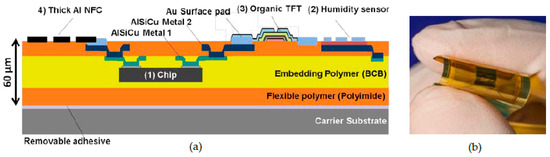
Figure 2.
The Chip-Film Patch (CFP) technology. (a) Schematic of the foil technology enabling the ultra-thin sensor system. (b) Embedded 20-µm thick silicon chip.
3. Results and Discussion
In order to test the HySiF components, the humidity sensors are released from the Si carrier wafer and connected to 400-µm and 30-µm thick readout chips. Similarly, the passive LC on-foil components are connected to a Si chip, which implements the near field communication protocols (NF4 chip from the company EM microelectronics). The NFC operation is then verified using a NFC-enabled smart phone. Finally, the organic TFTs are characterized on the flexible substrate.
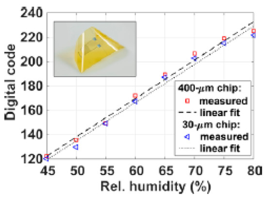
Figure 2 presents the measurement results for the on-foil capacitive relative humidity sensor when connected to the readout chips assembled in a ceramic package. They show similar response in terms of linearity, where the calculated coefficient of determination (R2) equals to 0.9868 and 0.9867 for the 400-µm and 30-µm chips, respectively. The readout circuit comprises a programmable charge amplifier and a 10-bit ADC. The 5 × 5 mm2 on-foil sensor and reference capacitors (nominal value about 30 pF) are arranged in half-bridge configuration that is excited with two out of phase square wave signals. During the CMOS chip design, expected stress levels inside the CFP package are considered in simulation as statistical variations such as for other process parameters.
Table 1 summarizes electrical characterization results of different inductors fabricated on the flexible substrate. Note that as the metal trace density increases, the stress induced on the flexible substrate increases which leads to warpage and difficulties during the foil release from the carrier substrate. That’s why it is better to use less number of turns and minimum trace width that satisfy the inductor quality factor requirements.

Table 1.
The on-foil inductors electrical characterization.
Figure 4a shows the measured inductance of an on-foil loop (25 × 35 mm2, 10 turns, trace width and spacing = 100 µm, trace thickness = 3 µm). At different bending radii, the uniaxial tensile strain acting on the loop increases the inductor average diameter, hence the inductance value increases. For NFC communication, this inductance shift needs to be taken into consideration in circuit design.
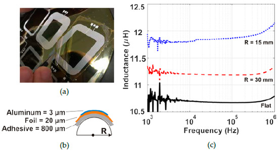
Figure 4.
The on-foil inductors. (a) Mechanical release of the inductors from the carrier wafer. (b) Illustration of the foil stack during bending, while highlighting each layer thickness. (c) Electrical characterization using LCR meter at different bending strain.
The NF4 chip includes an on-chip resonant capacitor of 14 pF, which is usually not enough to achieve an optimized NFC resonance frequency of 14.5 MHz. That’s why, on-foil capacitors were fabricated which have the same structure as the reference capacitors used for the half-bridge in the humidity sensor readout.
In large-area sensor systems, several readout channels are usually implemented and time-multiplexed to achieve an area and power-efficient silicon chip. However, the number of sensors could be extended if an off-chip/on-foil multiplexer is implemented. Figure 5 shows the measured linearity of the on-foil p-type organic TFT analog switch (channel width = 200 µm, channel length from 4 µm to 80 µm, mobility = 1.3 cm2/Vs, threshold voltage = −1 V). The switch linearity improves as the channel length increases, thus dictating a lower switching frequency for the readout chain.
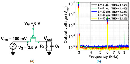
Figure 5.
(a) Measurement setup to show the linearity of the on-foil p-type organic TFT switches by measuring the total harmonic distortion. Sine-wave signal of frequency 3 kHz and amplitude of Vrms = 100 mV is applied to the source of the p-channel TFT and the drain is monitored using a spectrum analyzer as plotted in (b).
4. Conclusions
Towards the realization of a complete Hybrid Systems-in-Foil (HySiF), the design, fabrication and characterization of three important discrete ultra-thin flexible electronic components were investigated. First, the measurement results of an on-foil relative humidity (RH) sensor system showed consistent performance when interfacing with a ultra-thin readout chip (thinned down to ≈ 30 µm), compared to a typical chip prior to packaging (thickness ≈ 400 µm). Secondly, the electrical characterization of a 3-µm thick aluminum inductor loop showed the possibility for fabricating high quality Near Field Communication (NFC) antennas on the foil surface. Thirdly, and lastly, the static and dynamic parameters of on-foil organic Thin-Film Transistors (TFTs) were reported.
Author Contributions
This paper is based on discussions and collaboration among all the authors.
Acknowledgments
This work was funded by the German Federal Ministry of Education and Research (BMBF) as a part of the ParsiFAl4.0 project (#16ES0435). A due word of thanks goes to Hagen Klauk and Ute Zschieschang for the organic transistors fabrication.
Conflicts of Interest
The authors declare no conflict of interest. The founding sponsors had no role in the design of the study; in the collection, analyses, or interpretation of data; in the writing of the manuscript, and in the decision to publish the results.
References
- Afsar, Y.; Moy, T.; Brady, N.; Wagner, S.; Sturm, J.C.; Verma, N. Large-scale Acquisition of Large-area Sensors Using an Array of Frequency-hopping ZnO Thin-Film-Transistor Oscillators. ISSCC Dig. Tech. Pap. 2017, 256–257. [Google Scholar] [CrossRef]
- Moy, T.; Huang, L.; Rieutort-Louis, W.; Wu, C.; Cuff, P.; Wagner, S.; Sturm, J.C.; Verma, N. An EEG Acquisition and Biomarker-Extraction System Using Low-Noise-Amplifier and Compressive-Sensing Circuits Based on Flexible, Thin-Film Electronics. IEEE J. Solid-State Circ. 2016, 52, 309–321. [Google Scholar] [CrossRef]
- Quintero, A.V.; Molina-Lopez, F.; Smits, E.C.P.; Danesh, E.; Van den Brand, J.; Persaud, K.; Oprea, A.; Barsan, N.; Weimar, U.; De Rooij, N.F.; et al. Smart RFID Label with a Printed Multisensor Platform for Environmental Monitoring. Flex. Print. Electron. 2016, 1, 1–13. [Google Scholar] [CrossRef]
- Papadopoulos, N.P.; De Roose, F.; Van der Steen, J.P.J.; Smits, E.C.P.; Ameys, M.; Dehaene, W.; Genoe, J.; Myny, K. Toward Temperature Tracking With Unipolar Metal-Oxide Thin-Film SAR C-2C ADC on Plastic. IEEE J. Solid-State Circ. 2018, 1–10. [Google Scholar] [CrossRef]
- Alavi, G.; Sailer, H.; Albrecht, B.; Harendt, C.; Burghartz, J.N. Optimized Adaptive Layout Technique for Hybrid Systems in Foil. Proc. EMPC 2017. [Google Scholar] [CrossRef]
- Elsobky, M.; Mahsereci, Y.; Yu, Z.; Richter, H.; Burghartz, J.N.; Keck, J.; Klauk, H.; Zschieschang, U. Ultra-Thin Smart Electronic Skin Based on Hybrid System-in-Foil Concept Combining Three Flexible Electronics Technologies. Electron. Lett. 2018, 54, 338–340. [Google Scholar] [CrossRef]
- Elsobky, M.; Albrecht, B.; Richter, H.; Burghartz, J.N.; Ganter, P.; Szendrei, K.; Lotsch, B.V. Ultra-Thin Relative Humidity Sensors for Hybrid System-in-Foil Applications. IEEE Sens. 2017. [Google Scholar] [CrossRef]
- Elsobky, M.; Elattar, M.; Alavi, G.; Letzkus, F.; Richter, H.; Burghartz, J.N.; Strecker, M.; Klauk, H.; Zschieschang, U. A Digital Library for a Flexible Low-Voltage Organic Thin-Film Transistor Technology. Org. Electron. 2017, 50, 491–498. [Google Scholar] [CrossRef]


Publisher’s Note: MDPI stays neutral with regard to jurisdictional claims in published maps and institutional affiliations. |
© 2018 by the authors. Licensee MDPI, Basel, Switzerland. This article is an open access article distributed under the terms and conditions of the Creative Commons Attribution (CC BY) license (https://creativecommons.org/licenses/by/4.0/).