Proceeding Paper

Low-Offset In-Plane Sensitive Hall Arrangement †

Institute of Robotics at Bulgarian Academy of Sciences, Sofia, Bulgaria
*
Author to whom correspondence should be addressed.
Presented at the Eurosensors 2018 Conference, Graz, Austria, 9–12 September 2018.
Proceedings 2018, 2(13), 713; https://doi.org/10.3390/proceedings2130713
Published: 21 December 2018
(This article belongs to the Proceedings of EUROSENSORS 2018)

Abstract

:
A novel in-plane sensitive Hall arrangement consisting of two identical n-Si three-contact (3C) elements and realized in a common technological process, is presented. In the solution, the minimization of the offset and its temperature drift is achieved by cross-coupling of the outer device contacts. This terminals’ connection provides equalizing currents between the two substrates which strongly compensate the inevitable difference in the electrical conditions in the two parts of the arrangement. As a result, the residual offset of both integrated Hall elements at the output Vout(0) and its temperature drift are strongly minimized. The residual offset is about 160 times smaller than the single-configuration one. The obtained output voltage-to-residual offset ratio at sensitivity of SRI ≈ 98 V/AT is very promising, reaching 6 × 10³ at temperature T = 40 °C and induction 1 T. As a result, increased metrological accuracy for numerous applications is achieved. For a first time through the novel arrangement a suppression of sensitivity in the presence of external magnetic field could be achieved in order to obtain permanent offset information. This is one of the key results in the Hall device investigation.

1. Introduction

Offset is an enormous disadvantage of Hall effect devices with differential output measured in the absence of a magnetic-field only. This drawback changes the sensor’s output in an unpredictable way. The most probable reasons for the occurrence of the offset are: the electrical asymmetry (resulting from geometrical errors in the masks’ positioning in the technological production process) caused by the geometry in the location of the peripheral contacts with respect to the central one, the inevitable structure damages and imperfections of the silicon substrates, the mechanical and temperature stress and strain (caused most often by the chip’s capsulation) and more, [1,2,3,4,5]. This problem is crucial in many areas of sensor applications, like robotics, mechatronics, navigation, contactless automation, position sensors, angular displacement detection, automobile industry including ABS systems. For example, the 3C, 4C, 5C and 6C in-plane sensitive Hall devices have relatively high offset, larger than the offset of the orthogonal Hall plates, alongside with substantial temperature drift. These defects seriously impede measurement accuracy. The most common solutions removing these problems are very complicated and costly—for example, dynamic offset cancelation by various current spinning techniques. Such approach does not match the ordinary Hall element and its transduction principle. This paper suggests a novel simple, but sufficiently effective in-plane sensitive silicon Hall arrangement, ensuring low offset and low temperature drift.

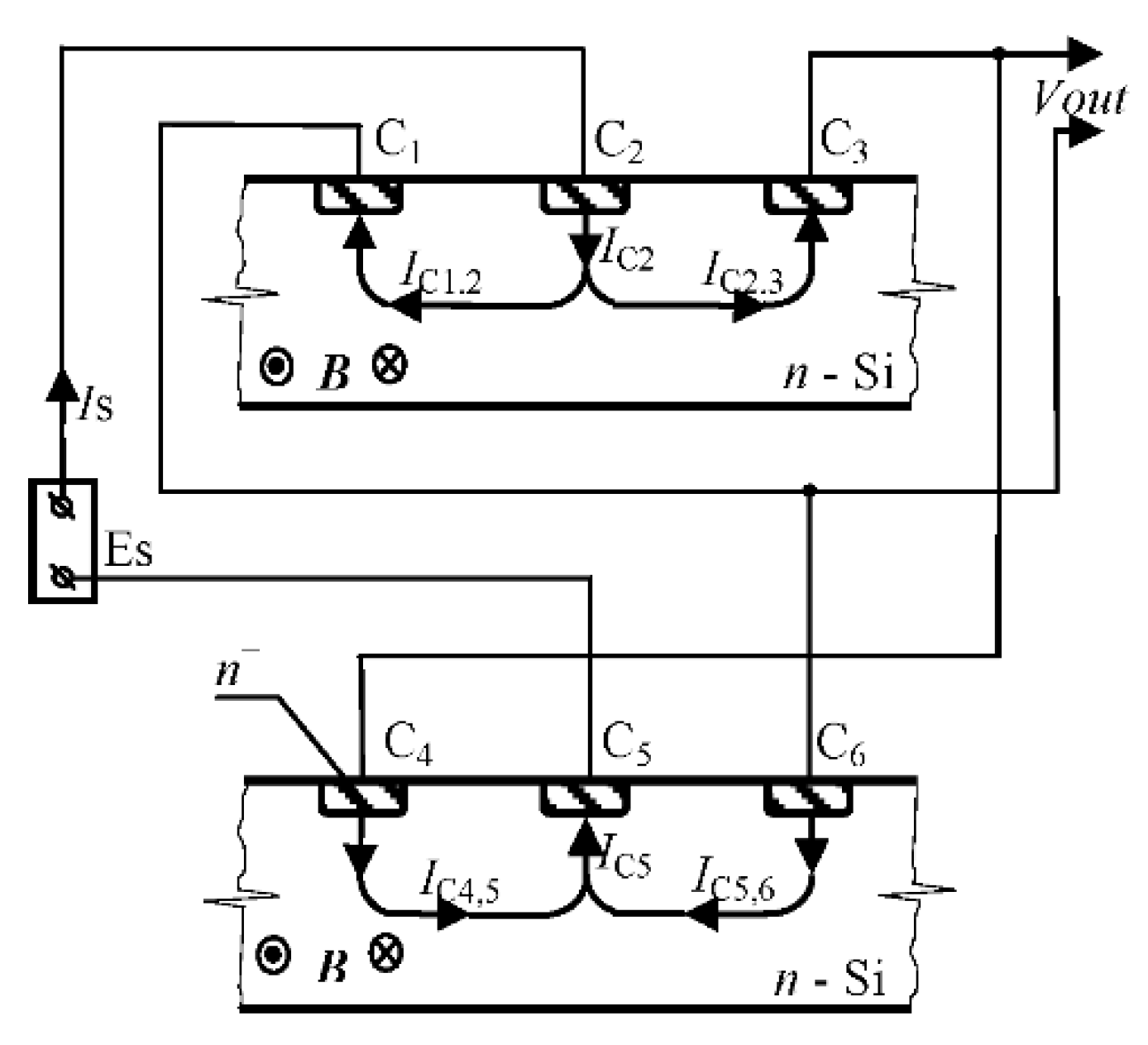
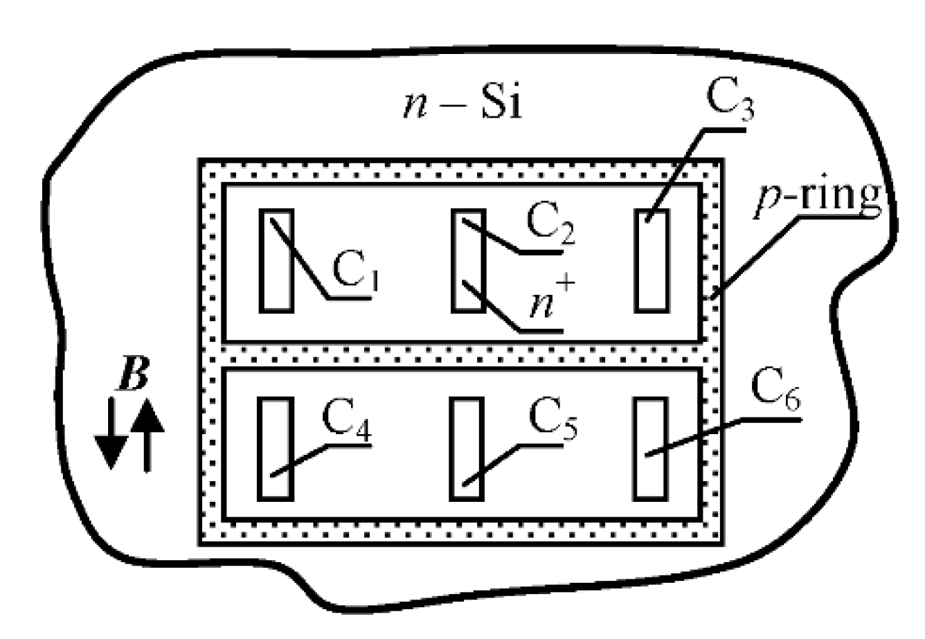
2. Sensor Layout and Operation Principle
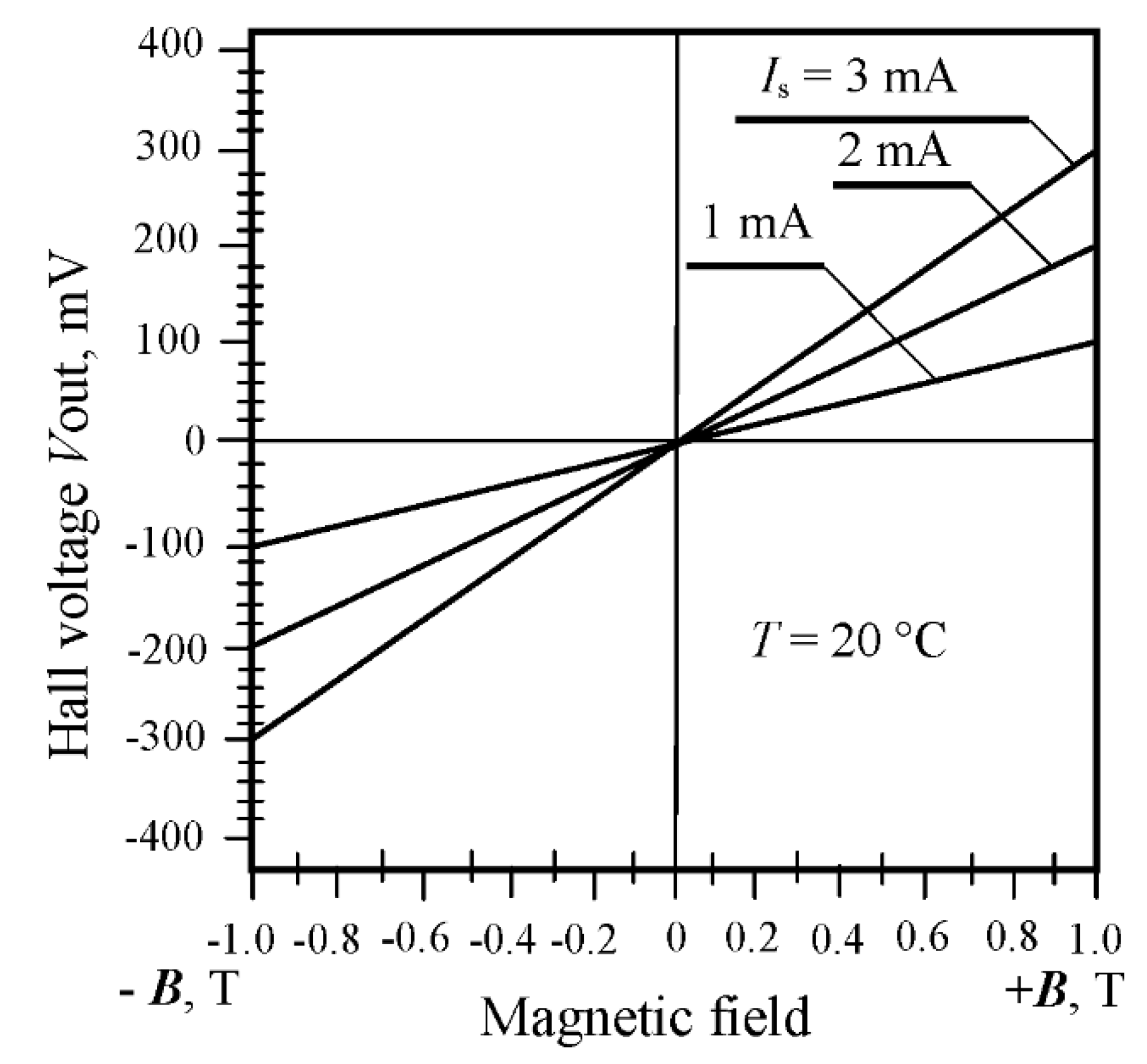
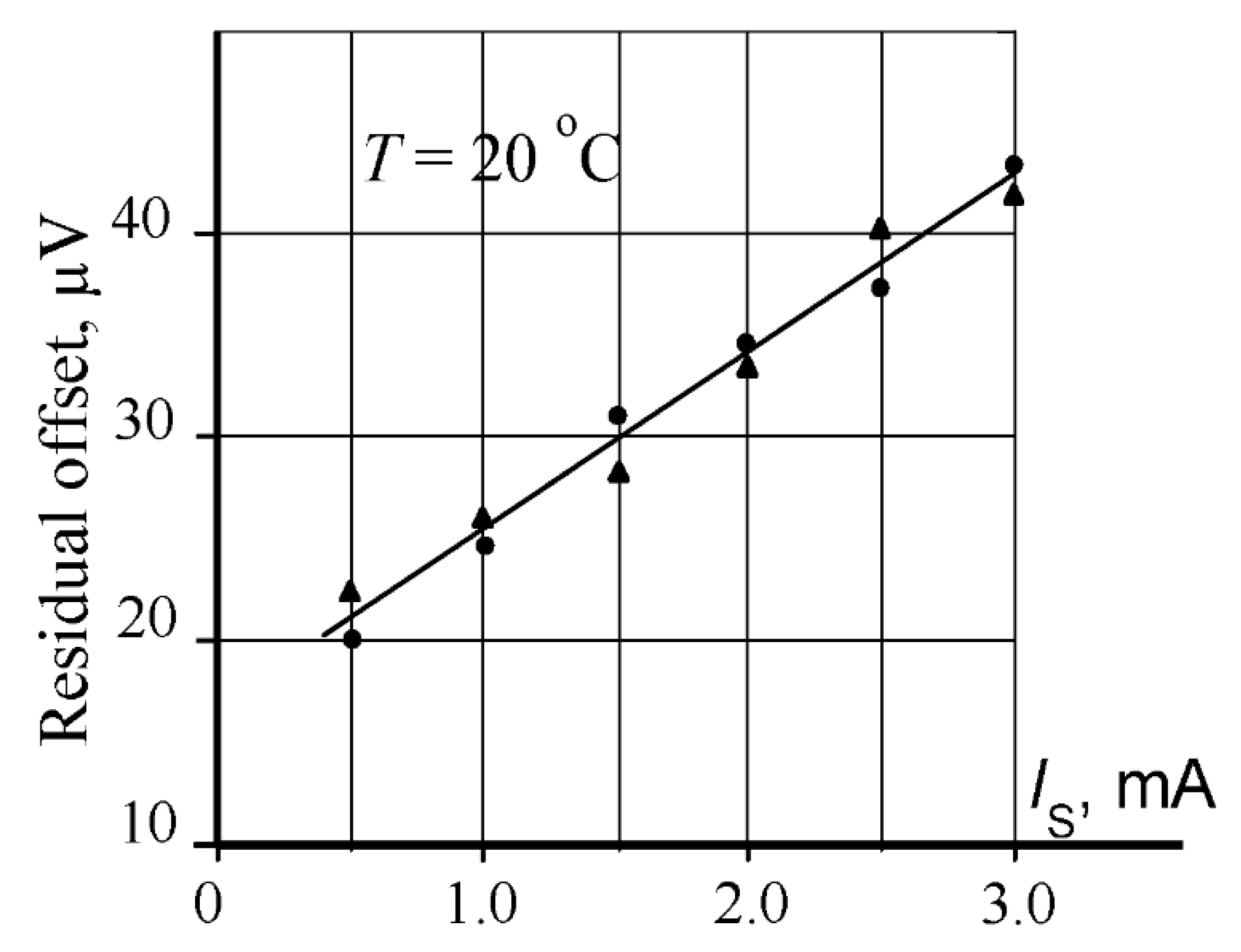
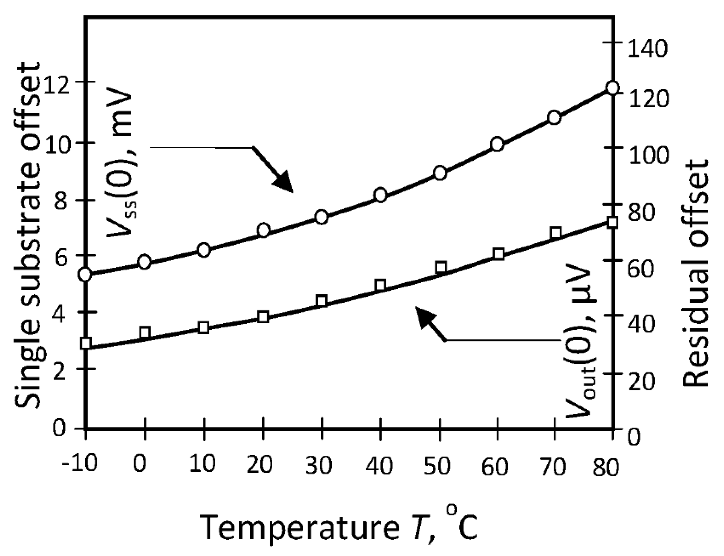
The novel Hall configuration consists of two identical n-Si substrates, parallel to one another, Figure 1. On the top surface of each of the structures, three identical rectangular n+-n contacts are formed—C1, C2, C3 and C4, C5, C6, respectively, Figure 1 and Figure 2. The supply source ES is connected to both middle contacts C2 and C5.
The differential output Vout(B) of the Hall arrangement is between contacts C1 and C3 (or C4 and C6). The measured magnetic field B is parallel to the long sides of the contacts. When power supply Es is fed, by cross-coupling of the outer contacts C1–C6 and C3–C4, in the substrate bulks, two equal and opposite currents IC2 and −IC5 start to flow, IC2 = |−IC5| ≡ Is, Figure 1.
The experimental prototype has been fabricated using part of the processing steps applied in bipolar IC technology. The resistivity of the n-Si substrate is ρ ≈ 7.5 Ω.cm (n0 ≈ 4 × 1015 cm−3). Similarly to [6], four masks are used. The size of contacts C1 … C6 is 50 × 10 μm2, the distance between the central and the outer contacts is 25 μm and the width of the р-ring on the chip surface is about 30 μm. The penetration of the current trajectories into the n-Si substrates reaches a depth of 30–40 μm. The operational volume of the device is about 100 × 70 × 40 μm3 [7].
The action of the in-plane Hall arrangement is the following. When the two central contacts C2 and C5 are connected to supply ES, in the bulk of the two substrates, two opposite-direction and equal-value current components, IC2,1 and −IC2,3, IC5,4 and −IC5,6, respectively, flow. The planar central contacts C2 and C5, as well as the outer contacts C1 and C3, and C4 and C6 respectively, form equipotential planes where, in the absence of magnetic field, В = 0, the currents flowing through them are always perpendicular to the upper side of the chip. The current lines penetrate deep into their volumes. The depth at fixed concentration of the dopant donors ND in the substrates depends on the ratio between the width of the central contacts and the distance between them and the outer electrodes. The maximal value of the depth in n-Si at ND ≈ 1015 cm−3 constitutes about 40 μm. Therefore, the trajectories of the carriers are curvilinear, [1,2,3]. In the general case, at the output Vout(0), in the absence of magnetic field, В = 0, parasitic output offset Vout(0) ≠ 0 is available, which is not related with metrology. In the proposed solution, Figure 1, the minimization and/or removal of the offset is achieved by the direct connection of contacts C1 and C6, and C3 and C4, respectively. This short-circuit results in the flowing of compensation equalizing currents between the two identical Hall structures in the absence of magnetic field, В = 0.
The application of the measured magnetic field В ≠ 0 in parallel to the long sides of the contacts results in lateral deflection of the current lines along the entire length of their non-linear trajectory. This is due to the action of Lorentz forces FL,i, FL = qVdr × B, where q is the electron’s elementary charge, and Vdr is the vector of the mean drift velocity of the electrons in the substrates, [1,3]. Of key importance is the effect of the force FL on the components I2 and I5 through the central contacts C2 and C5. As a result of the Lorentz deflection, the non-linear trajectories shrink and expand, respectively. For this reason, on planar contacts C1 and C3, and C4 and C6, Hall potentials VH,C1(B) = VH,C6(B) and −VH,C4(B) = −VH,C3(B) are generated simultaneously. Actually, the measured magnetic field В disturbs the electric symmetry of the current trajectories with respect to the central contacts. Therefore, on the differential output Vout(B) of the arrangement, Figure 1, Hall voltage VH(B) ≡ VH,C1–C3(B) arises. This signal is a linear and odd function of the strength of the supply current and the magnetic field В. On the respective outer contacts C1–C6 and C3–C4, Hall potentials with the same sign and value are generated. The solution from Figure 1 reduces drastically the offset. The configuration features yet another advantage, which is one of the key results in this investigation. If contacts C1 and C4, and C3 and C6 are connected using electronic switch, for example, then Hall potentials (Hall voltage) compensation (nulling) occurs:
VH,C1(B) = |−VH,C4(B)| and VH,C3(B) = |−VH,C6(B)|.
As a result, the magnetosensitivity in the two identical configurations is lacking. The only remaining signal is the parasitic offset. In this case the output is between contacts C1 and C3 or C4 and C6. The purpose is to achieve at any time information about the negative offset in output signal, regardless the available external magnetic field. Such approach is proposed for the first time in the sensorics of Hall elements.

3. Results

The output characteristics Vout(B) of the microdevice are presented in Figure 3. The obtained relative current magnetosensitivity is SRI ≈ 98 V/AT. The non-linearity NL does not exceed 0.6% within the range 0.5 T ÷ −0.5 T.
The temperature dependences of the single-substrate offset Vss(0) and the residual offset Vout(0) of the arrangement, at a supply current Is = 3 mA and field B = 0 in the temperature range – 10 ≤ T ≤ 80 °C, are shown in Figure 4. The temperature coefficient of the offset drift reaches no more than 0.1%/°C. The obtained output voltage-to-residual offset ratio, for example at T = 40 °C, reaches around 6 × 10³ at induction B = 1 T. This is a very promising result. At first approximation the residual offsets measured at field B = 0 and induction B = 0.35 T are on a straight line, Figure 5.

4. Conclusions

The new solution is a combination of innovative circuit technology and device design through which, with one supply current, high magnetosensitivity in both substrates is generated. The original connection of the outer contacts reduces substantially the inevitable parasitic offset by flowing of equalizing currents.
For the first time in the Hall effect sensors, through the new arrangement, complete suppression of magnetosensitivity in the presence of magnetic field could be achieved. This result follows from the identity of the two 3C structures and the common supply current. This allows to be obtained at any time information about the value and sign of the offset for the purpose of its extraction from the sensor’s output signal. The proposed in-plane sensitive Hall arrangement features multi-purpose industrial applicability.

Acknowledgments

This work was supported by Sci. Res. Fund under project No. DN 07/18-15.12.2016.

References

  1. Roumenin, C. Solid State Magnetic Sensors; Elsevier: Amsterdam, The Netherlands, 1994. [Google Scholar]
  2. Kaufmann, T. On the Offset and Sensitivity of CMOS-Based Five-Contact Vertical Hall Devices; MEMS Technology and Engineering; Der Andere Verlag: Uelvesbull, Germany, 2013; Volume 21, p. 147. [Google Scholar]
  3. Lozanova, S.V.; Roumenin, C.S. Parallel-field silicon Hall effect microsensors with minimal design complexity. IEEE Sens. J. 2009, 9, 761–766. [Google Scholar] [CrossRef]
  4. Schurig, E.; Schott, C.; Besse, P.-A.; Popovic, R.S. CMOS integrated vertical Hall sensor with low offset. In Proceedings of the 16th European Conference on Solid-State Transducers, Prague, Czech Republic, 15–18 September 2002; pp. 868–871. [Google Scholar]
  5. Schurig, E.; Schott, C.; Besse, P.-A.; Demierre, M.; Popovic, R.S. 0.2 mT residual offset of CMOS integrated vertical Hall sensors. Sens. Actuators A 2004, 110, 98–104. [Google Scholar] [CrossRef]
  6. Schott, C.; Popovic, R. Integrated 3-D Hall magnetic field sensor. In Proceedings of the Transducers’99, Sendai, Japan, 7–10 June 1999; Volume 1, pp. 168–171. [Google Scholar]
  7. Lozanova, S.; Noykov, S.; Ivanov, A.; Roumenin, C. In-plane magnetosensitive double Hall device. In Proceedings of the 2017 XXVI International Scientific Conference Electronics (ET), Sozopol, Bulgaria, 13–15 September 2017; pp. 19–21. [Google Scholar]
Figure 1. The novel Hall arrangement.
Proceedings 02 00713 g001
Figure 2. Top-view of the Hall architecture.
Proceedings 02 00713 g002
Figure 3. Output characteristics Vout(B).
Proceedings 02 00713 g003
Figure 4. Temperature dependences of single offset Vss(0) and residual offset Vout(0) at a supply Is = 3 mA.
Proceedings 02 00713 g004
Figure 5. Residual offsets at field B = 0 (●) and induction B = 0.35 T (▲).
Proceedings 02 00713 g005
Publisher’s Note: MDPI stays neutral with regard to jurisdictional claims in published maps and institutional affiliations.

