SPM—SEM Investigations of Semiconductor Nanowires for Integrated Metal Oxide Gas Sensors †

 , , and
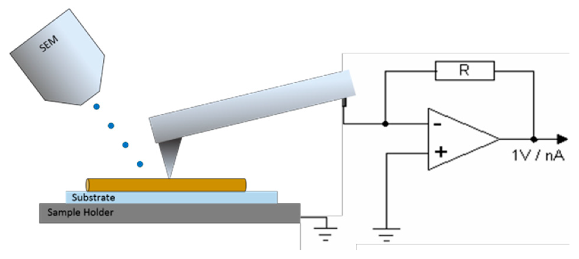
Abstract
:1. Introduction
2. Materials and Methods
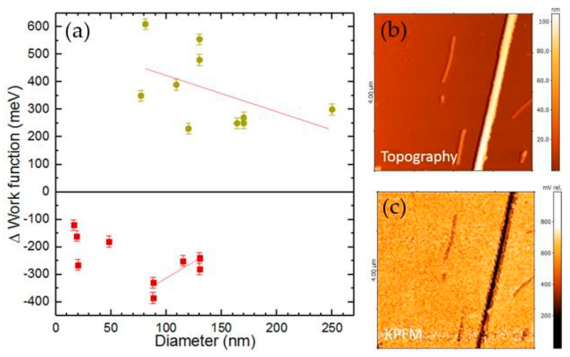
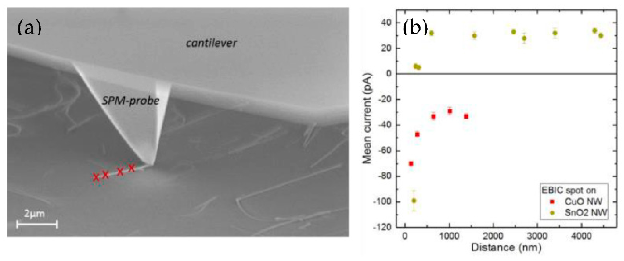
3. Results
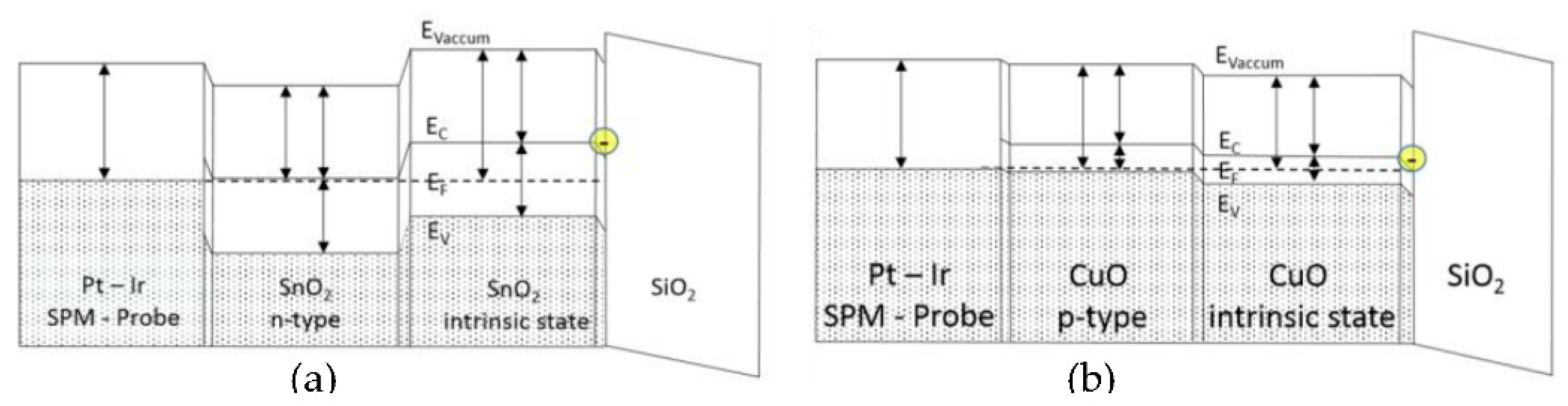
4. Discussion
5. Conclusions
Author Contributions
Acknowledgments
Conflicts of Interest
References
- Barsan, N.; Koziej, D.; Weimar, U. Metal oxide-based gas sensor research: How to? Sens. Actuators B Chem. 2007, 121, 18–35. [Google Scholar] [CrossRef]
- Wimmer-Teubenbacher, R.; Lackner, E.; Krainer, J.; Steinhauer, S.; Koeck, A. Gas Sensor Devices based on CuO- and ZnO- Nanowires directly synthesized on silicon substrate. MRS Adv. 2016, 1, 817–823. [Google Scholar] [CrossRef]
- Comini, E.; Sberveglieri, G. Metal oxide nanowires as chemical sensors. Mater. Today 2010, 13, 36–44. [Google Scholar] [CrossRef]
- Kolmakov, A.; Zhang, Y.; Cheng, G.; Moskovits, M. Detection of CO and O2 using tin oxide nanowire sensors. Adv. Mater. 2003, 15, 997–1000. [Google Scholar] [CrossRef]
- Heiderhoff, R.; Cramer, R.M.; Balk, L.J. High resolution electron beam induced current measurements in an SEM-SPM hybrid system by tip induced barriers. Inst. Phys. Conf. Ser. 1995, 149, 189–194. [Google Scholar]
- Chen, J.T.; Zhang, F.; Wang, J. CuO nanowires synthesized by thermal oxidation route. J. Alloys Compd. 2008, 454, 268–273. [Google Scholar] [CrossRef]
- Glavatskikh, I.A.; Kortov, V.S.; Fitting, H.J. Self-consistent electrical charging of insulating layers and metal- insulator-semiconductor structures. J. Appl. Phys. 2001, 89, 440–448. [Google Scholar] [CrossRef]


Publisher’s Note: MDPI stays neutral with regard to jurisdictional claims in published maps and institutional affiliations. |
© 2018 by the authors. Licensee MDPI, Basel, Switzerland. This article is an open access article distributed under the terms and conditions of the Creative Commons Attribution (CC BY) license (https://creativecommons.org/licenses/by/4.0/).
Share and Cite
Leitgeb, V.; Fladischer, K.; Hitzel, F.; Sosada-Ludwikowska, F.; Krainer, J.; Wimmer-Teubenbacher, R.; Köck, A. SPM—SEM Investigations of Semiconductor Nanowires for Integrated Metal Oxide Gas Sensors. Proceedings 2018, 2, 701. https://doi.org/10.3390/proceedings2130701
Leitgeb V, Fladischer K, Hitzel F, Sosada-Ludwikowska F, Krainer J, Wimmer-Teubenbacher R, Köck A. SPM—SEM Investigations of Semiconductor Nanowires for Integrated Metal Oxide Gas Sensors. Proceedings. 2018; 2(13):701. https://doi.org/10.3390/proceedings2130701
Chicago/Turabian StyleLeitgeb, Verena, Katrin Fladischer, Frank Hitzel, Florentyna Sosada-Ludwikowska, Johanna Krainer, Robert Wimmer-Teubenbacher, and Anton Köck. 2018. "SPM—SEM Investigations of Semiconductor Nanowires for Integrated Metal Oxide Gas Sensors" Proceedings 2, no. 13: 701. https://doi.org/10.3390/proceedings2130701
APA StyleLeitgeb, V., Fladischer, K., Hitzel, F., Sosada-Ludwikowska, F., Krainer, J., Wimmer-Teubenbacher, R., & Köck, A. (2018). SPM—SEM Investigations of Semiconductor Nanowires for Integrated Metal Oxide Gas Sensors. Proceedings, 2(13), 701. https://doi.org/10.3390/proceedings2130701