Abstract
This paper proposes a new method for characterization of 2D materials under the precisely specified conditions. It is achieved by integration of a 2D material as a field effect transistors structures with a piezoelectric resonator. Properties of the 2D material can be mechanically adjusted by the resonator. It results in the independent and precise control of an amplitude of induced mechanical strain, its modulating frequency, which all influence the 2D material properties. The electrical field required to measure 2D material field effect transistors will not be affected by the vibrations, thus giving us a chance to perform the precise measurement of the electrical properties of the 2D material. This approach has a great potential for measuring and monitoring cells, enzymes, nucleic acids, deoxyribonucleic acid and ribonucleic acid. It can be also used for measurement of toxic, combustive or waste gases.
1. Introduction
In the past two years, there has been great interest in 2D monoelemental materials beyond graphene, such as group IVA elements: silicene and germanene and group VA elemets:phosphorene, arsenene, and antimonene [1]. The utilization of 2D materials for field effect transistor (FET) based devices was investigated more than decade ago for graphene by studying the electric field effect in this 2D material. Since then, graphene has been extensively studied, including graphene-based FETs for various sensing applications. The drain current value through FET structure can be affected by modulating the electron mobility in the substrate either mechanically by stretching the 2D material or chemically by modifying its properties. The first can be used for mechanical sensing and the second for chemical or biochemical sensing.
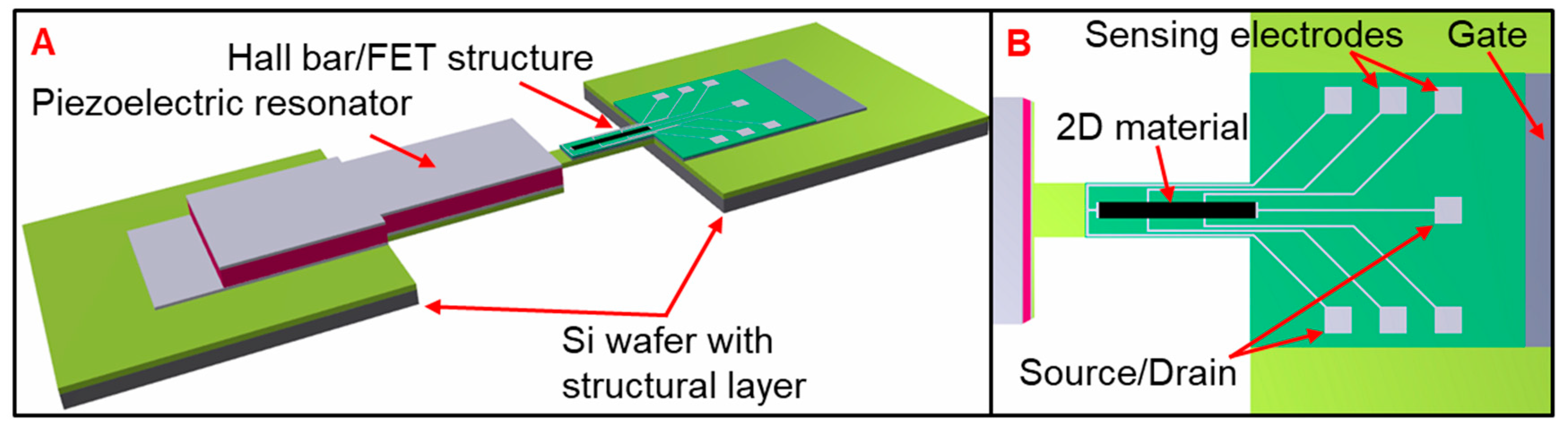
Here we propose a new method for characterization of 2D materials under well-defined conditions. The fundamental concept is based on the integration of 2D material as Hall bar/FET structures with the piezoelectric resonator. The Hall bar/FET structures are used to measure modulated 2D material electrical properties as a function of induced strain and/or electric field (Figure 1A). The FET allows to modulate the concentration of charge carriers by the gate voltage. The entire structure is fabricated on a Si (100) wafer substrate using planar technology.

Figure 1.
Proof of concept and principle of proposed structure (not to scale): (A) MEMS piezoelectric resonator mechanically linked to stretching Hall bar/FET structure; (B) The detail of stretching part with 2D material using Hall Bar/FET structure for electric measurements of 2D material properties.
Our unique structure gives us an opportunity to control and to decouple the mechanical and the electrical phenomena. Mechanical oscillations of the 2D material are induced by an independent AC bias applied at the piezoelectric resonator without affecting the gate voltage of the FET in contrary to previously published work [2]. We are able to measure the electrical Hall bar/FET properties separately with the induced strain as a parameter. This decoupling significantly increases the measurement precision. It allows application of a small gate voltage at the FET to modulate the Fermi level simultaneously with a high voltage at the resonator to optimize the conditions. This approach could be applied on different structure designs containing a number of piezoelectric resonators linked mechanically to the Hall bar/FET structures in different directions. It will allow us to induce uniaxial or biaxial strain in 2D material and to determine its influence on 2D material properties and its utilization as a sensor.
2. Numerical Model of Piezoelectric Resonator
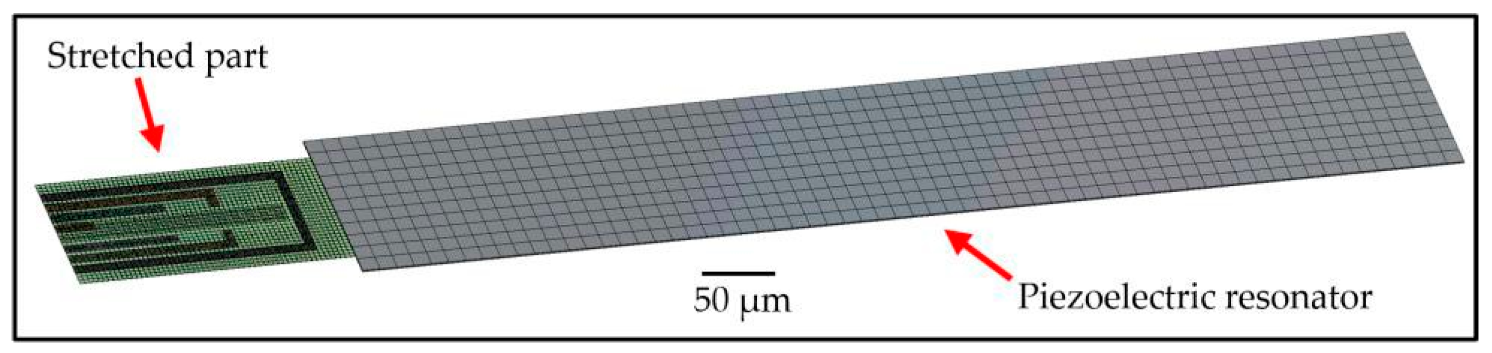
We performed a structural finite element method (FEM) analyses of a single clamped SiO2/Ti/AlN/Ti/Al piezoelectric resonator linked mechanically to a single clamped stretching device representing graphene Hall Bar/FET structure made of SiO2/Al/SiO2/Ti/Pt. The appropriate properties of material were set for each part of the model. We used the SOLID226 element (20-node brick) for numerical discretization (Figure 2 supporting piezoelectric analysis.

Figure 2.
The meshed model of single clamped piezoelectric resonator linked mechanically to single clamped stretching device representing 2D material Hall Bar/FET structure.
The coupled solution of the electrostatic and structural solver was realized via the piezoelectric matrix [e]:
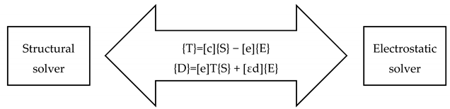
where {T} is the stress vector, [c] is the elastic stiffness matrix, {S} is the elastic strain vector, [e] is the piezoelectric matrix, {E} is the electric field intensity vector, {D} is the electric flux density vector, and [εd] is the dielectric permittivity matrix.
Firstly, we performed modal analysis determining eigenfrequencies of the entire system. These results served as input for boundary conditions of piezoelectric harmonic analysis. The actual values of deformation, induced strain and maximal stress were determined in harmonic analysis.
3. Results and Discussion
Modal analysis was used to determine the natural frequencies and mode shapes of a structure. The natural frequencies and mode shapes are important parameters in the design of a structure for dynamic load conditions. In order to achieve the good convergence of the ANSYS solver, a numerical damping of 0.005 was used [3].
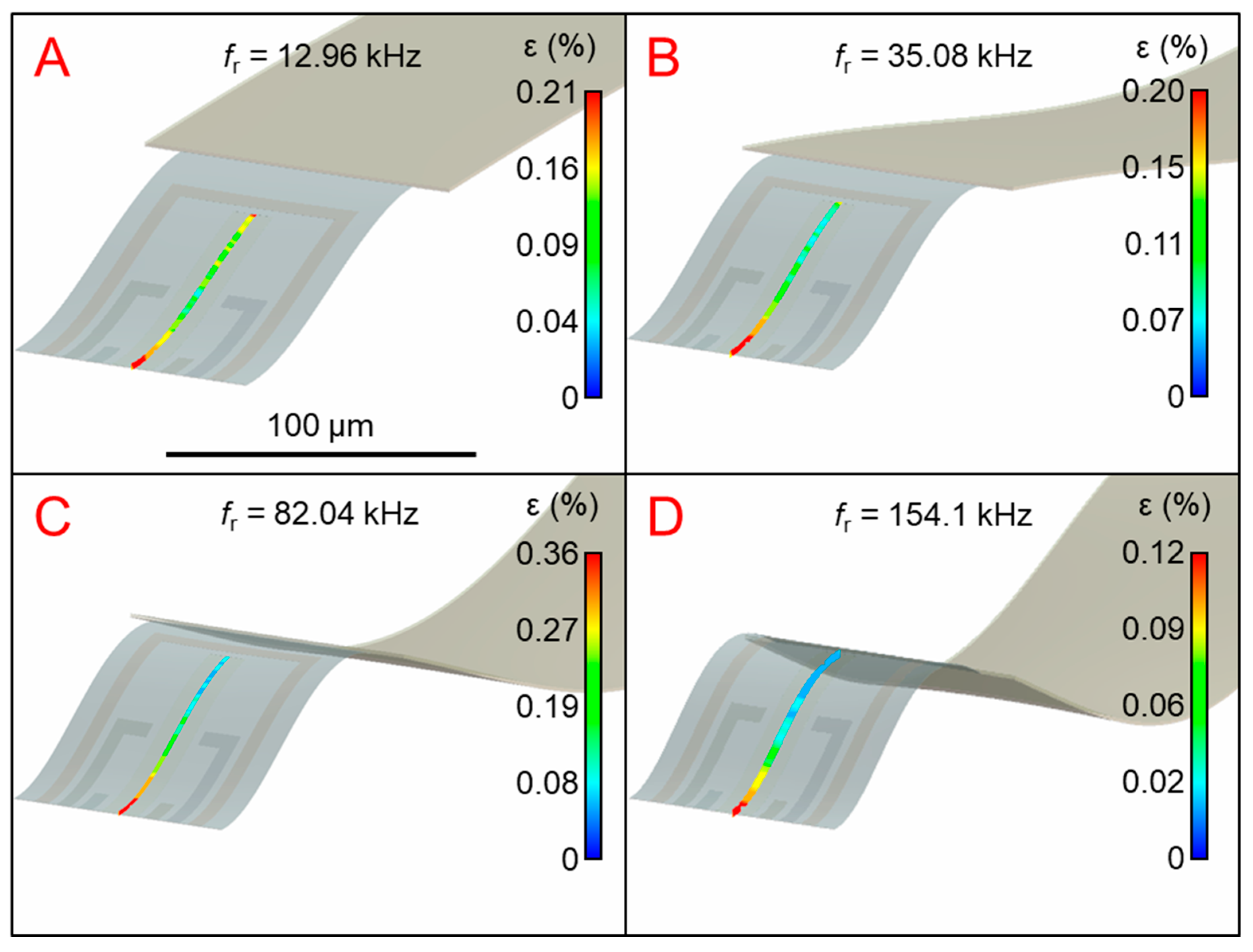
FEM structural analysis (Figure 3) shows the influence of resonator bending on induced strain (ε) into the stretched part which is linked mechanically to the resonator part. The size of resonator part was 600 μm × 100 μm and the size of stretched part was 100 μm × 75 μm. The harmonic analysis was performed in range from 0 to 200 kHz and four resonant modes (Figure 3) were found. The 3rd and 6th resonance modes from the modal analysis did not show any response due to different bending mode (torsional).
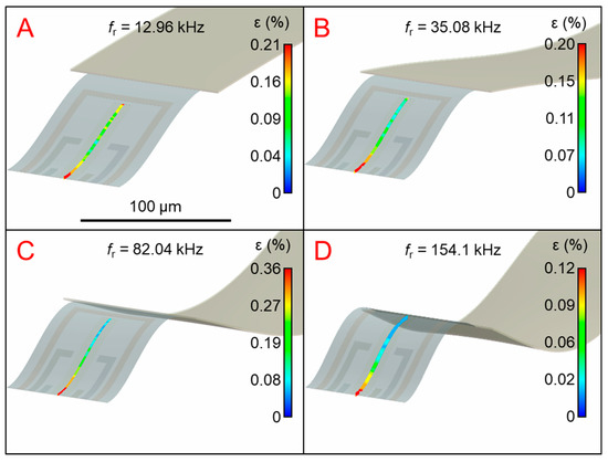
Figure 3.
The strain distribution in 2D material placed on the single clamped stretching part. The stretching part is linked mechanically to the single clamped piezoelectric resonator: (A) 1st mode at frequency of 12.96 kHz; (B) 2nd mode at frequency of 35.08 kHz; (C) 4th mode at frequency of 82.04 kHz; (D) 5th mode at frequency of 154.1 kHz. The black scale bar is the same for all figures.
We simulated the strain distribution as a function of AC bias voltage up to 20 V applied to electrodes of the piezoelectric resonators. We obtained the maximum value of the induced strain ≈0.36% in dynamic mode for a path placed as the 2D material (Figure 3C). The induced strain was relatively lower than that achieved by other researchers [2,4]. On the other hand, the induced strain can be modulated by tuning the resonator frequency. The strain value can be further increased by changing the dimensions and shapes of resonators. Longer and narrower part of resonator together with the shorter stretching part increases rapidly the maximum induced strain in 2D material.
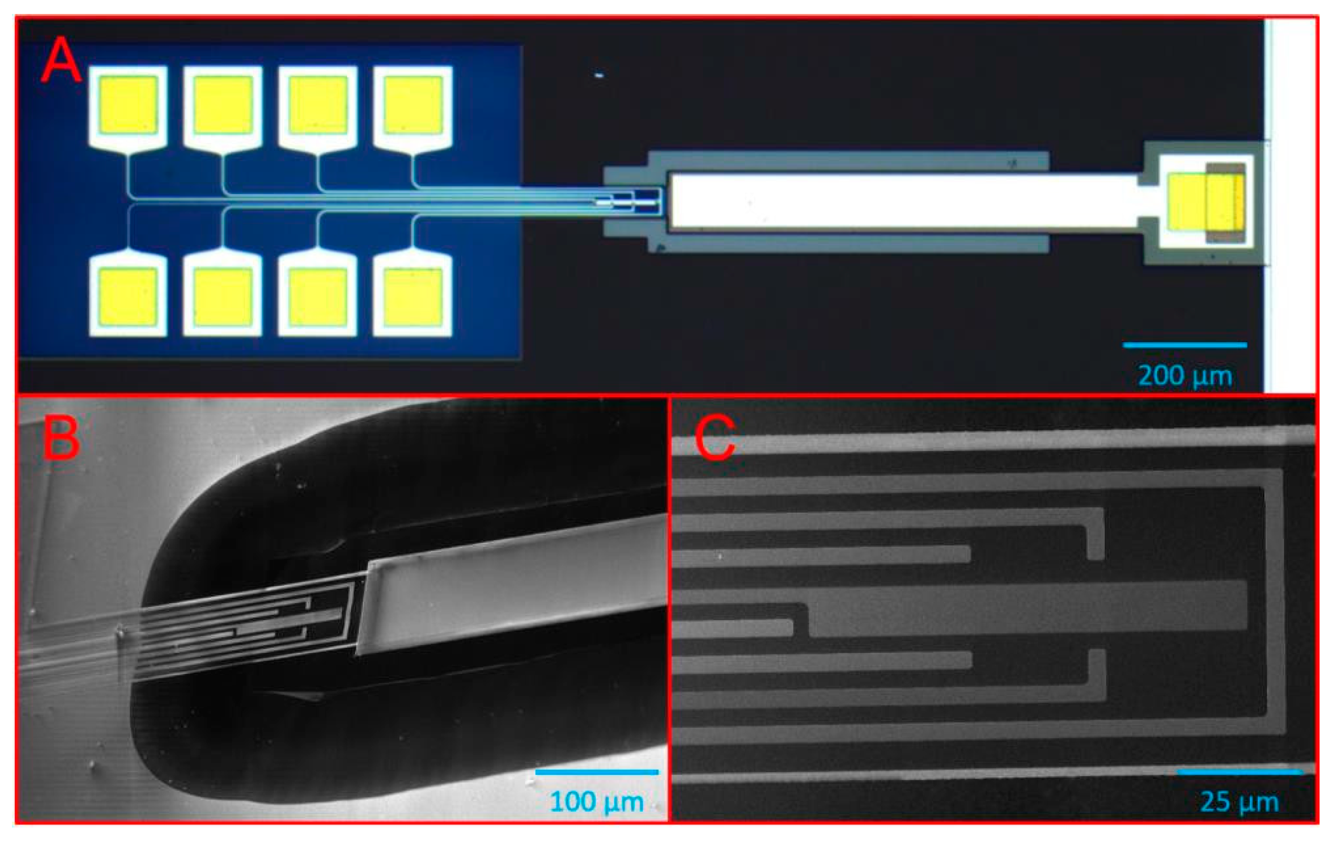
The simulated structures were fabricated (Figure 4) and will be tested in the future with new 2D materials.
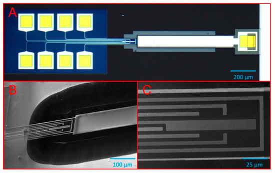
Figure 4.
Fabricated structure for 2D material characterization: (A) An optical image of entire structure; (B) scanning electron microscope analysis of released resonator; (C) the detail of stretched part with electrodes.
4. Conclusions
This paper proposed the idea of modulating the properties of 2D material monolayer. We simulated structures for the 2D material characterization. It will be possible to precisely control the induced strain for any 2D material. We obtained value of induced strain of 0.36% for frequency of 82.04 kHz. This can be modified by changing the dimensions of the resonator and the stretched part. The simulated structures were fabricated using the standard planar technology processes and will be used for 2D material characterization.
Acknowledgments
We acknowledge the support of the Grant Agency of the Czech Republic under the contract GJ18-06498Y, the support of the Ministry of Education, Youth and Sports of the Czech Republic under NPU I programme (projects No. LO1210 and LO1401), and the support of BUT No. FEKT/STI-J-17-4136. This research work has been carried out in the Centre for Research and Utilization of Renewable Energy (CVVOZE) and in the SIX Center of BUT.
Conflicts of Interest
The authors declare no conflict of interest. The founding sponsors had no role in the design of the study; in the collection, analyses, or interpretation of data; in the writing of the manuscript, and in the decision to publish the results.
References
- Gablech, I.; Pekárek, J.; Klempa, J.; Svatoš, V.; Sajedi-Moghaddam, A.; Neužil, P.; Pumera, M. Monoelemental 2D materials-based field effect transistors for sensing and biosensing: Phosphorene, antimonene, arsenene, silicene, and germanene go beyond graphene. TrAC Trends Anal. Chem. 2018, 105, 251–262. [Google Scholar] [CrossRef]
- Dong, J.; Liu, S.; Fu, Y.; Wang, Q. Investigation of strain-induced modulation on electronic properties of graphene field effect transistor. Phys. Lett. A 2017, 381, 292–297. [Google Scholar] [CrossRef]
- Putnik, M.; Cardanobile, S.; Nagel, C.; Degenfeld-Schonburg, P.; Mehner, J. Simulation and modelling of the drive mode nonlinearity in MEMS-gyroscopes. Procedia Eng. 2016, 168, 950–953. [Google Scholar] [CrossRef]
- Choi, S.-M.; Jhi, S.-H.; Son, Y.-W. Controlling Energy Gap of Bilayer Graphene by Strain. Nano Lett. 2010, 10, 3486–3489. [Google Scholar] [CrossRef] [PubMed]
Publisher’s Note: MDPI stays neutral with regard to jurisdictional claims in published maps and institutional affiliations. |
© 2018 by the authors. Licensee MDPI, Basel, Switzerland. This article is an open access article distributed under the terms and conditions of the Creative Commons Attribution (CC BY) license (http://creativecommons.org/licenses/by/4.0/).