Novel Design of an Extremely Miniaturized Accelerometer Based on Quantum Tunneling Effect †

Abstract
:1. Introduction
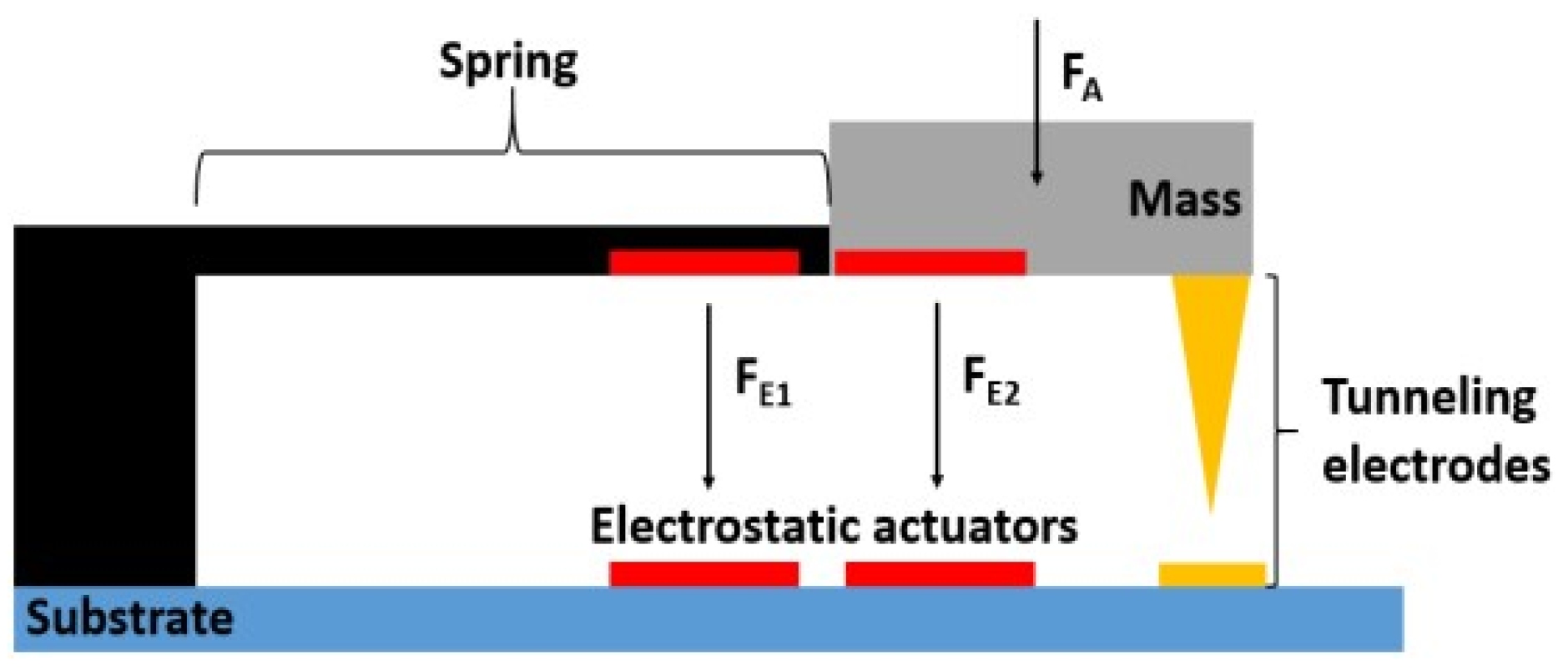
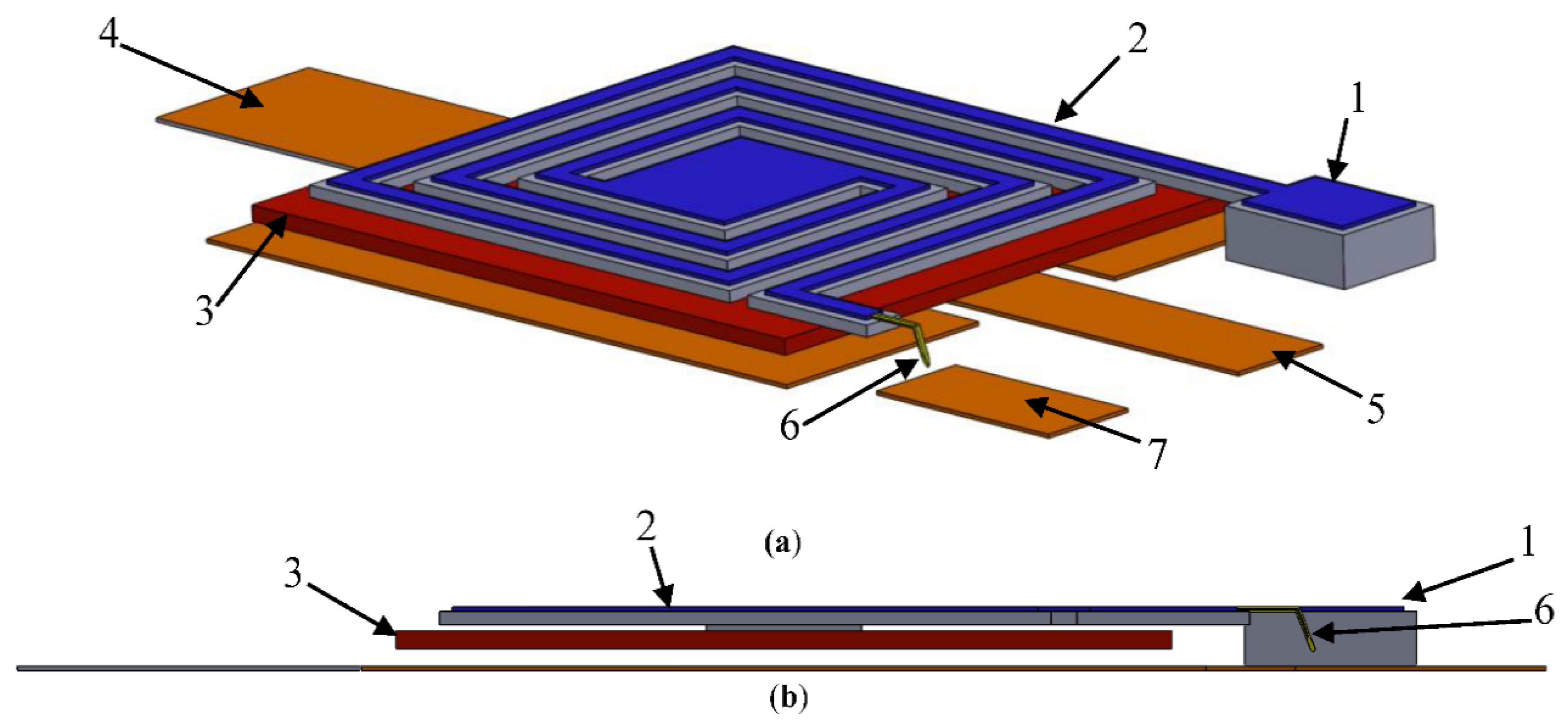
2. Sensor Structure
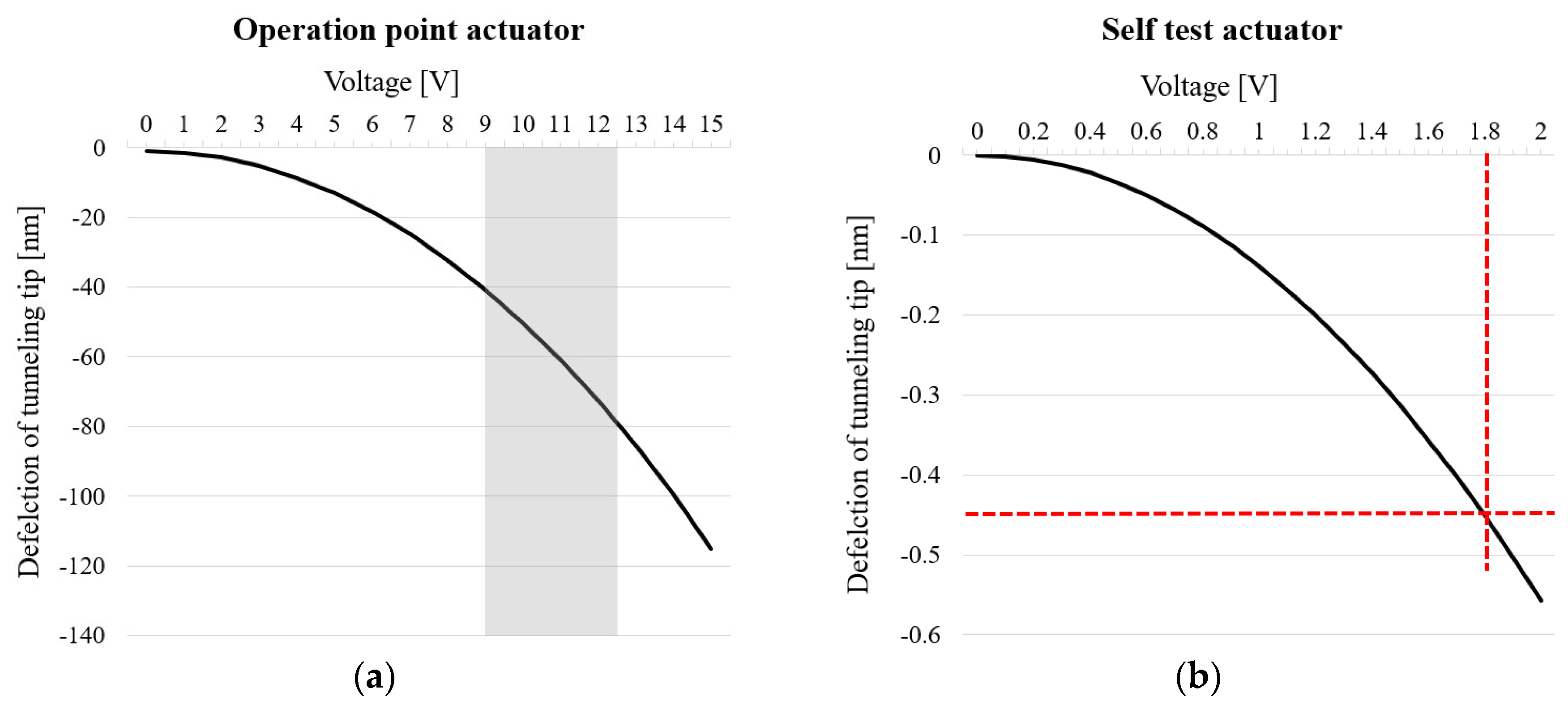
3. Electrostatic Actuators
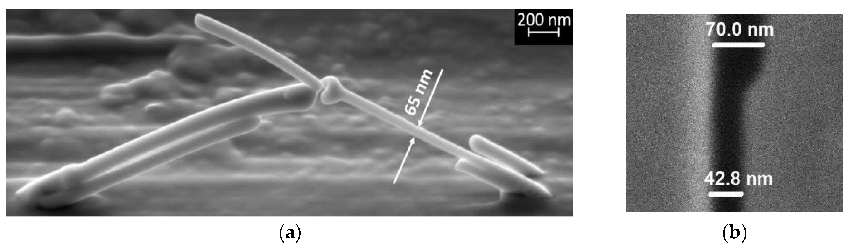
4. Tunneling Tip
5. Conclusion and Summary
Acknowledgments
Conflicts of Interest
References
- Rockstad, H.K.; Tang, T.K.; Reynolds, J.K.; Kenny, T.W.; Kaiser, W.J.; Gabrielson, T.B. A miniature, highsensitivity, electron tunneling accelerometer. Sens. Actuators A Phys. 1996, 53, 227–231. [Google Scholar] [CrossRef]
- Liu, C.-H.; Kenny, T.W. A High-Precision, Wide-Bandwidth Micromachined Tunneling Accelerometer. J. Micromech. Syst. 2001, 10, 425–433. [Google Scholar] [CrossRef]
- Zavracky, P.M.; McClelland, B.; Warner, K.; Wang, J.; Hartley, F.; Dolgin, B. Design and process considerations for a tunneling tip accelerometer. J. Micromech. Microeng. 1996, 6, 352358. [Google Scholar] [CrossRef]
- Miao, M.; Hu, Q.; Hao, Y.; Dong, H.; Wang, L.; Shi, Y.; Shen, S. A bulk micromachined Si-on-glass tunneling accelerometer with out-of-plane sensing capability. In Proceedings of the IEEE International Conference on Nano/Micro Engineered and Molecular Systems, Bangkok, Thailand, 16–19 January 2007. [Google Scholar]
- Strobelt, T. Hochauflösende Beschleunigungssensoren mit Tunnelstrecke. Ph.D. Thesis, University of Stuttgart, Stuttgart, Germany, 3 July 2000. [Google Scholar]
- Kobayashi, D.; Hirano, T.; Furuhata, T.; Fujita, H. An Integrated lateral tunneling unit. In Proceedings of the IEEE Micro Electro Mechanical Systems, Travemunde, Germany, 4–7 February 1992. [Google Scholar]
- Kubena, R.L.; Atkinson, G.M.; Robinson, W.P.; Stratton, F.P. A new miniaturized surface micromachined tunneling accelerometer. IEEE Electron Device Lett. 1996, 17, 306–308. [Google Scholar] [CrossRef]
- Patra, S.; Bhattacharyya, T.K. Design and Fabrication of micromachined tunneling accelerometers with micro-g resolution and their comparison. In Proceedings of the International Workshop on Electron Devices and Semiconductor Technology, Mumbai, India, 1–2 June 2009. [Google Scholar]
- Daniel, J.H.; Moore, D.F. A microaccelerometer structure fabricated in silicon-on-insulator using a focused ion beam process. Sens. Actuators A Phys. 1999, 73, 201–209. [Google Scholar] [CrossRef]

Publisher’s Note: MDPI stays neutral with regard to jurisdictional claims in published maps and institutional affiliations. |
© 2018 by the authors. Licensee MDPI, Basel, Switzerland. This article is an open access article distributed under the terms and conditions of the Creative Commons Attribution (CC BY) license (https://creativecommons.org/licenses/by/4.0/).
Share and Cite
Haub, M.; Hummel, S.; Bogner, M.; Sandmaier, H. Novel Design of an Extremely Miniaturized Accelerometer Based on Quantum Tunneling Effect. Proceedings 2018, 2, 1045. https://doi.org/10.3390/proceedings2131045
Haub M, Hummel S, Bogner M, Sandmaier H. Novel Design of an Extremely Miniaturized Accelerometer Based on Quantum Tunneling Effect. Proceedings. 2018; 2(13):1045. https://doi.org/10.3390/proceedings2131045
Chicago/Turabian StyleHaub, Michael, Sebastian Hummel, Martin Bogner, and Hermann Sandmaier. 2018. "Novel Design of an Extremely Miniaturized Accelerometer Based on Quantum Tunneling Effect" Proceedings 2, no. 13: 1045. https://doi.org/10.3390/proceedings2131045
APA StyleHaub, M., Hummel, S., Bogner, M., & Sandmaier, H. (2018). Novel Design of an Extremely Miniaturized Accelerometer Based on Quantum Tunneling Effect. Proceedings, 2(13), 1045. https://doi.org/10.3390/proceedings2131045