Proceeding Paper

Flatness Improvement of Double-Sided Magnetic Film for Narrow Gap Electromagnetic Energy Harvester †

Graduate School of Engineering, University of Hyogo, Himeji 671-2280, Japan
*
Author to whom correspondence should be addressed.
Presented at the Eurosensors 2018 Conference, Graz, Austria, 9–12 September 2018.
Proceedings 2018, 2(13), 1043; https://doi.org/10.3390/proceedings2131043
Published: 11 December 2018
(This article belongs to the Proceedings of EUROSENSORS 2018)

Abstract

:
This paper reports the design, modeling and preliminary fabrication result of the flatness improved magnetic film on a silicon structure for narrow-gap electromagnetic (EMG) vibration energy harvester (VEH). The harvester has double-sided corrugated shape silicon vibration mass with 15 µm-thick NdFeB permanent magnet. The narrower air-gap between the magnetic film and a counter coil electrode the higher output power. While the sputtered magnetic film shows good characteristics equivalent to a bulk magnet, it hinders to reduce the air-gap because the silicon structure was curved by its high residual stress. Applying the double-sided magnet to our previous device, the curvature radius of moving mass with 15 µm-thick NdFeB film was improved from 5.3 m to 40.1 m because of the stress compensation. With the narrowed 2 µm air-gap device, the resulting simulated output power is 48 µW that is 190 times as large as previous device.

1. Introduction

The IoT (Internet of things) and the AI (artificial intelligence) are most promising technologies for changing our world. Huge number of sensors and its systems will be spread and gather various data from our circumstances. To realize those systems, an autonomous power source is the most important issue [1,2]. Our group have been focused on to study a vibration energy harvester (VEH) for IoT power source by using MEMS (micro electromechanical systems) technology. Among these, an electromagnetic (EMG) type VEH has some advantages e.g., low output impedance, so there are many studies by using bulk magnet and coils [3]. Because of its difficulty for fine fabrication of permanent magnet in MEMS, there are very few researches of MEMS based EMG VEH. We have been developed a VEH with NdFeB/Ta multilayer film on a silicon MEMS structure. In order to obtain an alternating magnetic field, a sputtered magnetic film on a corrugated silicon MEMS structure was developed. Crossing by different distance between moving magnet and fixed coil, an electromotive force i.e., output voltage can be generated [4].
This paper reports the design, modeling and preliminary fabrication result of the flatness improved magnetic film on a silicon structure for narrow-gap EMG VEH. The harvester has double-side corrugated shape silicon vibration-mass with 15 µm-thick NdFeB permanent magnet. The narrower air-gap between the magnetic film and a counter coil electrode the higher output power. While the sputtered magnetic film shows good characteristics equivalent to a bulk magnet [5], it hinders to reduce the air-gap because the silicon structure was curved by its high residual stress. Applying the double-sided magnet to our previous device [6], the curvature radius of moving mass will be improved.

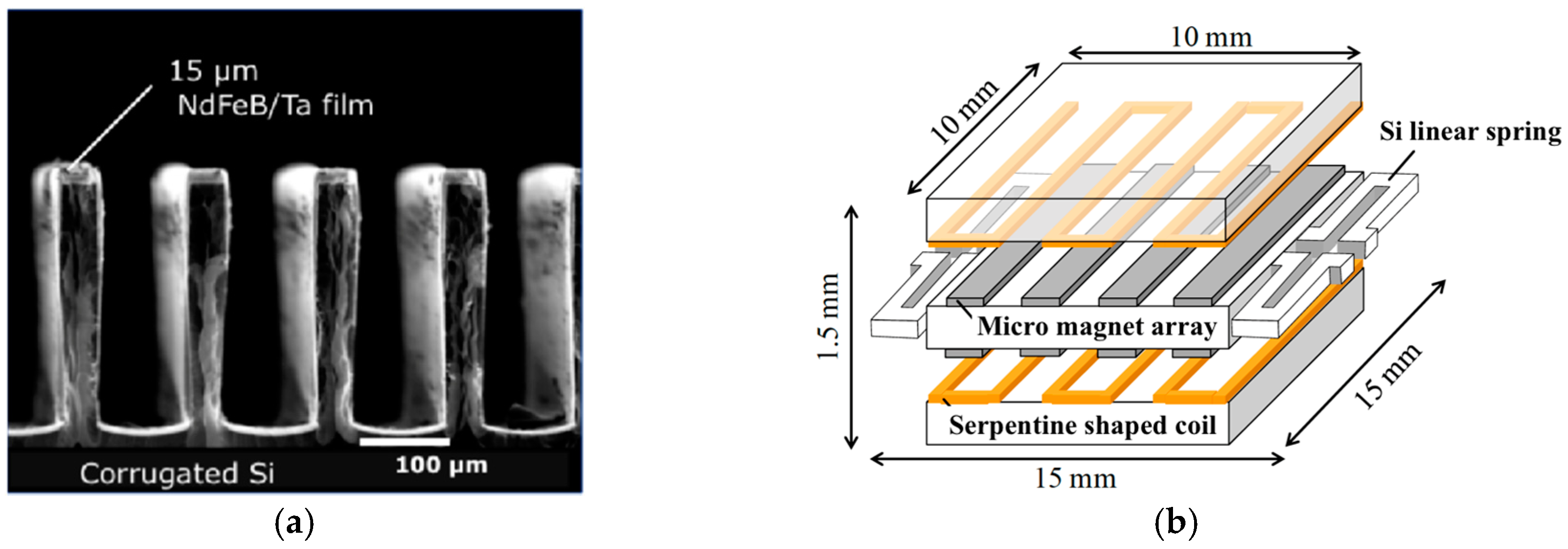
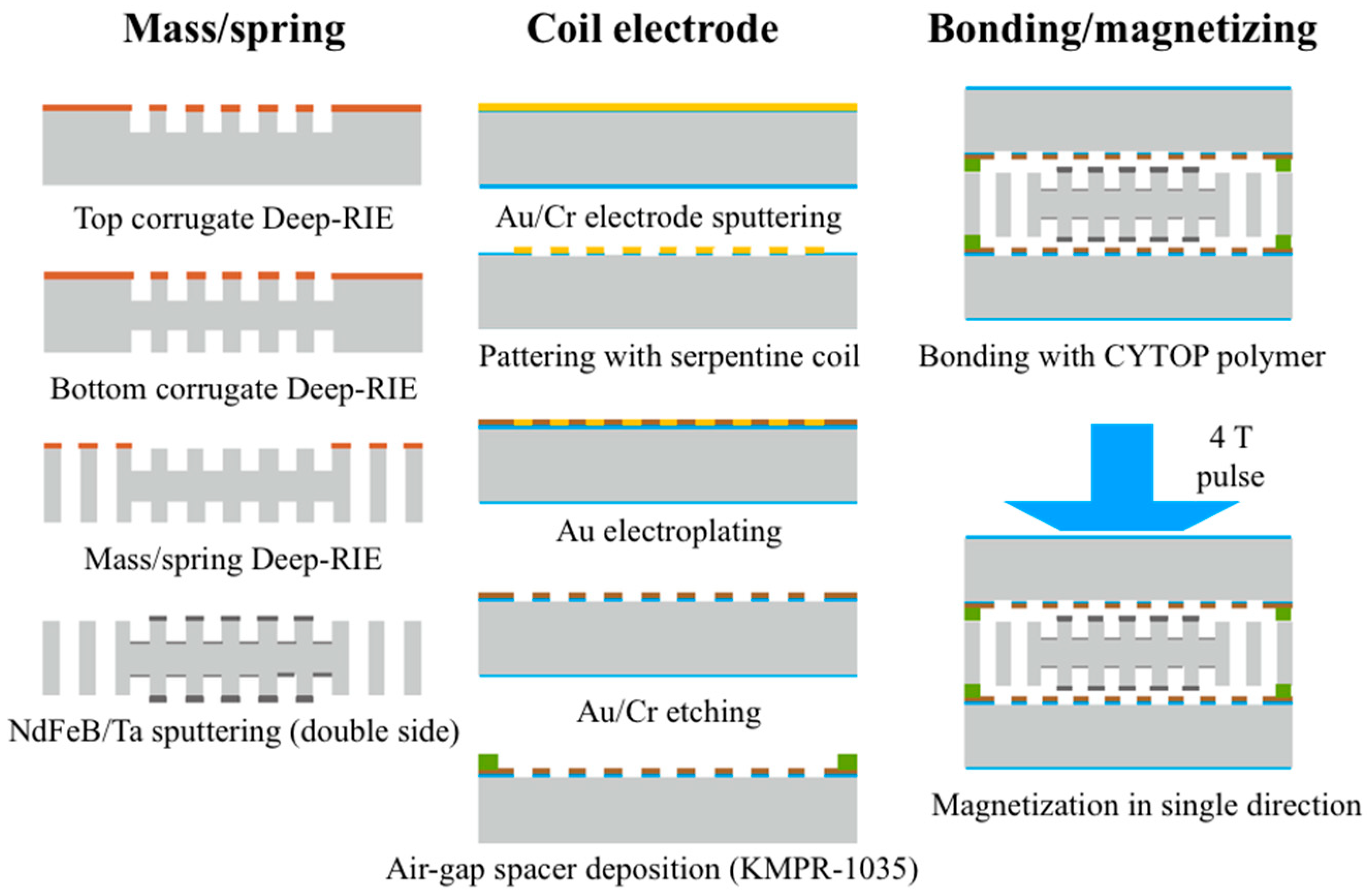
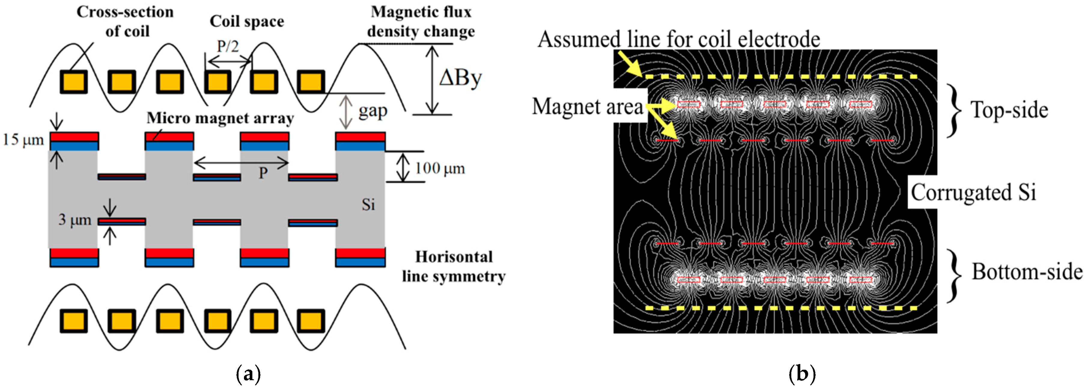
2. Double-Sided NdFeB EMG VEH

Figure 1a shows an SEM photograph of the sputtered NdFeB/Ta multilayer film on a silicon trench structure with depth of 300 µm by using a deep-RIE (reactive ion etching) process. A vital area of the magnetic film was deposited on the top and bottom of the trench structure. In order to improve magnetic characteristics, the process requires the sputtering temperature of higher than 600 °C. It induces large residual stress on the silicon wafer, and hinders to reduce the air-gap between the magnet and coil-electrode for large power harvesting. In addition, the stress limits a maximum thickness of sputtered NdFeB under 20 µm.
Figure 1b shows design of the novel double-sided EMG VEH. The 15 µm-thick sputtered NdFeB/Ta film on the 500 µm-thick silicon with 100 µm width and 200 µm depth trench. The chip size of 15 × 15 × 1 mm3 and vibration mass size of 10 × 10 × 0.5 mm3. Unlike in case of the previous device, the magnetic film is deposited on the movable mass and spring layer. Top and bottom side counter electrodes (serpentine shaped coil) are gold electroplated. The residual stress can be compensated by horizontal line symmetry design.
The fabrication process was based on the previous work; however, the double-sided NdFeB/Ta sputtering process was added (Figure 2). The magnetization process was performed after the bonding step by the pulse magnetizing with amplitude of 4 T in single-direction.
The surface contour profiles after the sputtering process were measured by 3D optical profilometer (ZYGO NewView6300, Canon, Tokyo, Japan). Figure 3 shows the comparison for flatness of (a) single-sided and (b) double-sided sputtered structures. The curvature radiuses of single and double-sided one can be calculated as 5.3 m and 40.1 m, respectively.

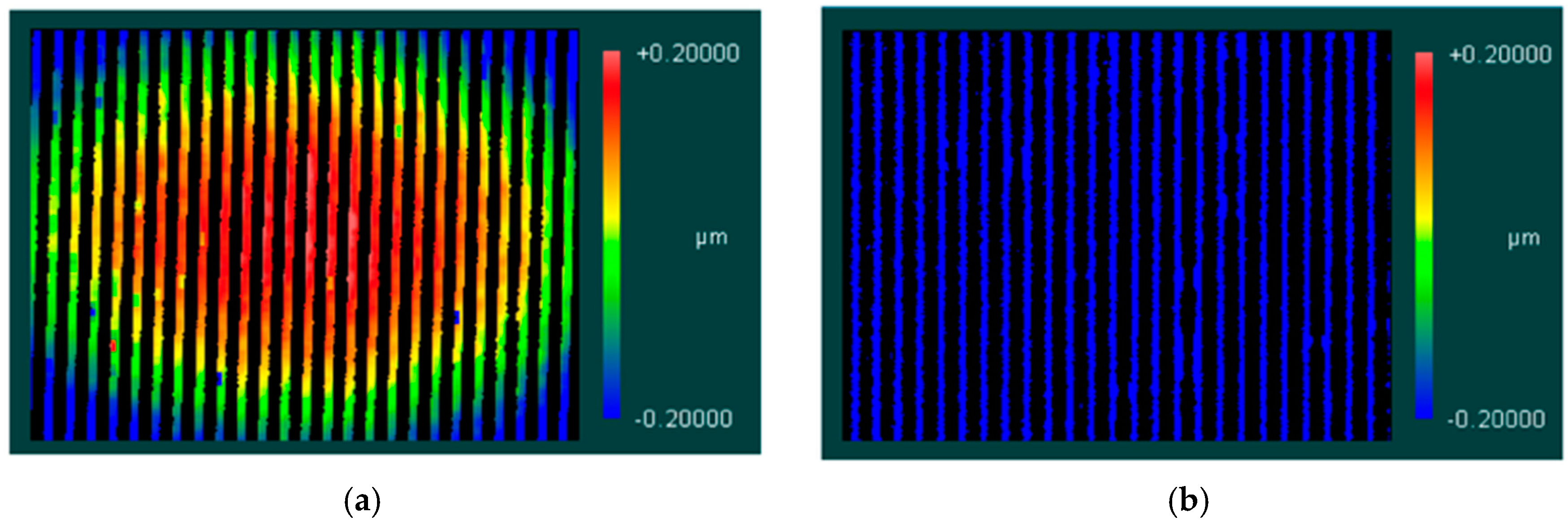
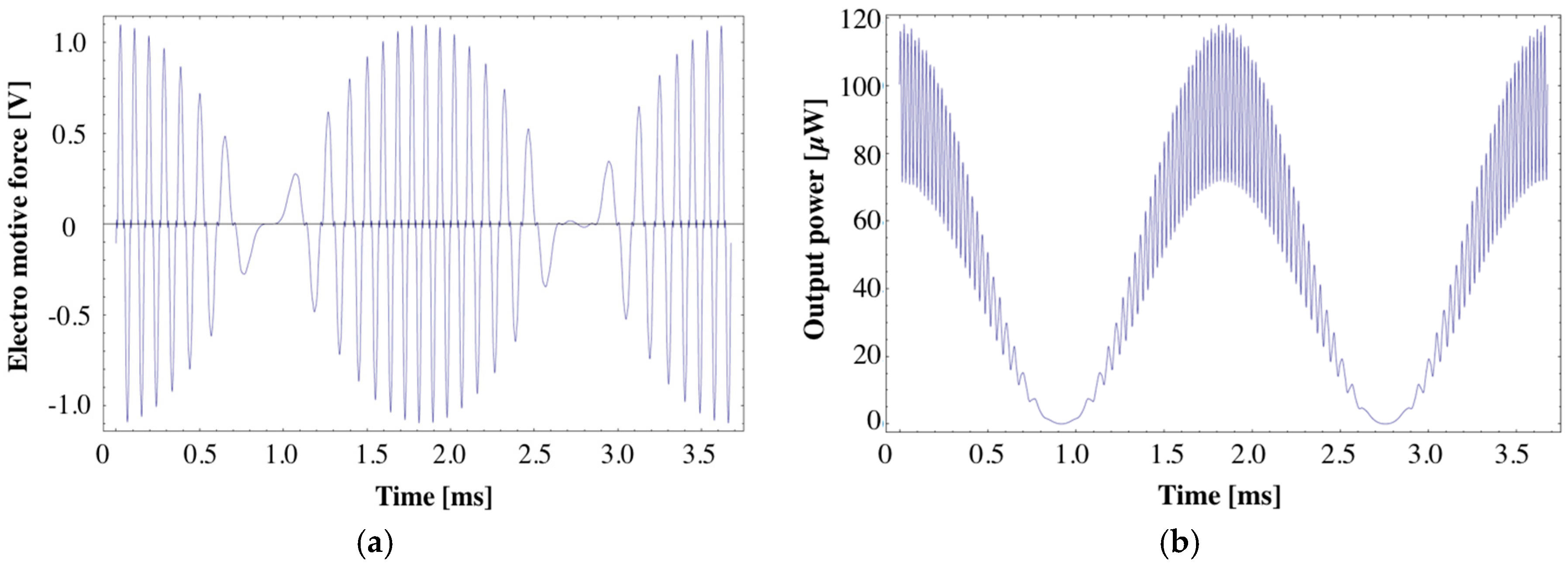
3. Harvesting Evaluation from Flatness Improved Structure

The flatness of the device was drastically improved by the stress conpensation. The maximum camber within 10 mm chip length was reduced to 0.3 µm. Thus, the assumed air-gap between the moving magnet and the stator coils can be reduced from 30 µm to 2 µm. The evaluated harvesting output by using an FEM analysis is obtained. Figure 4a shows simplified model for FEM analysis with 2 µm air-gap and optimum trench dimensions i.e., 28 µm line and space and 100 µm depth. The deferences of magnetic flux density, ∆B, from the assumed position for coil electrodes were calculated by the FEM analysis as shown in Figure 3b. Using the spacial data of ∆B, the output power can be expected to 47.8 µW with assumption of 2 µm air-gap, 4 µmp-p applied displacement, mechanical Q-factor of 470 (measured value from the previous work) and in resonant frequency of 272 Hz. The power is around 190 times as large as previous device. Figure 5a,b show simulated waveform of an electro motive force and simulated waveform of an output power with optimum load resistance, respectively.

4. Conclusions

Applying the double-sided magnet structure to the previous device, the curvature radius of moving mass with 15 µm-thick NdFeB/Ta film was improved from 5.3 m to 40.1 m because of the stress compensation. With the maximum camber of 0.3 µm, the resulting simulated output power of 48 µW from the 2 µm air-gap device is confirmed, which is 190 times as large as previous device.

Acknowledgments

This work was partly supported by JSPS (Japan Society for the Promotion of Science, Tokyo, Japan) KAKENHI Grant-in-Aid for Scientific Research(C) Number 16K06308.

References

  1. Shaikh, F.K.; Zeadallyc, S. Energy harvesting in wireless sensor networks. J. Renew. Sustain. Energy Rev. 2016, 55, 1041–1054. [Google Scholar] [CrossRef]
  2. Iannacci, J. Microsystem based Energy Harvesting (EH-MEMS): Powering pervasivity of the Internet of Things (IoT)—A review with focus on mechanical vibrations. J. King Saud Univ. 2017. [Google Scholar] [CrossRef]
  3. Wang, Y.; Zhang, Q.; Zhao, L.; Shkel, A.; Tang, Y.; Kim, E.S. Stackable Dual-Layer Coil Based on Wafer-Level Transfer Technique for Electromagnetic Energy Harvester. In Proceedings of the IEEE International Conference on Micro Electro Mechanical Systems, Shanghai, China, 24–28 January 2016; pp. 1264–1267. [Google Scholar]
  4. Yamaguchi, K.; Fujita, T.; Kanda, K.; Maenaka, K. Optimal Design of Electromagnetic Harvester with Sputtered Thin NdFeB/Ta Film and Considering Lorentz Force. IEEJ Trans. Sens. Micromach. 2016, 136, 72–76. [Google Scholar] [CrossRef]
  5. Uehara, M. Microstructure and permanent magnet properties of a perpendicular anisotropic NdFeB/Ta multilayered thin film prepared by magnetron sputtering. J. Magn. Magn. Mater. 2004, 284, 281–286. [Google Scholar] [CrossRef]
  6. Yamaguchi, K.; Tanaka, Y.; Fujita, T.; Takehira, N.; Sonoda, K.; Kanda, K.; Maenaka, K. Optimization and Experiment of Electromagnetic Energy Harvester by Using NdFeB Sputtered on High aspect-ratio Corrugated Si. J. Phys. Conf. Ser. 2014, 557, 012056. [Google Scholar] [CrossRef]
Figure 1. (a) SEM photograph of sputtered NdFeB/Ta multilayer film on 300 µm depth corrugated silicon; (b) Orthogonal schematic diagram of double-sided NdFeB magnetic film energy harvester.
Proceedings 02 01043 g001
Figure 2. Fabrication process flow of double-sided EMG VEH.
Proceedings 02 01043 g002
Figure 3. Surface contour profiles measured by 3D optical profilometer for (a) single-sided and (b) double-sided.
Proceedings 02 01043 g003
Figure 4. (a) Simplified model of double-sided EMG VEH for analysis; (b) Electromagnetic field simulation result from FEM (ANSYS, Canonsburg, PA, USA).
Proceedings 02 01043 g004
Figure 5. Simulated waveforms: (a) Electro motive force; (b) Harvesting output power.
Proceedings 02 01043 g005
Publisher’s Note: MDPI stays neutral with regard to jurisdictional claims in published maps and institutional affiliations.

