Proceeding Paper

Surface Plasmon Resonances in Sn: In2O3 Thin Films with Diffraction Grating †

1
Department of Electronics, Kyoto Institute of Technology, Kyoto 606-8585, Japan
2
WaferMaters, Inc., Dublin, CA 94568, USA
*
Author to whom correspondence should be addressed.
Presented at the Eurosensors 2018 Conference, Graz, Austria, 9–12 September 2018.
Proceedings 2018, 2(13), 1034; https://doi.org/10.3390/proceedings2131034
Published: 9 November 2018
(This article belongs to the Proceedings of EUROSENSORS 2018)

Abstract

:
We newly proposed transparent conductive oxide with diffraction grating structure as an excitation field of surface plasmon resonance working at near-infrared spectral region. We experimentally demonstrated the excitation of SPR using Sn-doped In2O3 films with micro-meter pitched diffraction grating. In this study, we considered the correlation between the grating pitch and the optical reflection spectra. Reflection spectra showed clear polarization properties in infrared spectral region, and the reflection edge has also correlation with the pitch of grating. From these results, the excitation of SPR grating was successfully demonstrated and the wavelength can be tuned by changing the grating pitch in infrared region.

1. Introduction

The sensing of molecules with high sensitivity, especially having complex structures such as biomolecules, can give detailed information on their molecule structure. Most of biomolecules contain the chemical bonds consist of C, O, N and H atoms. Their vibration frequencies often appear at near- and mid-infrared spectral region. One promising approach for increase in sensitivity is to amplify the interaction of molecular vibrations with infrared light by using surface plasmon resonance (SPR) enhancement [1]. It becomes possible by interacting the electric field comes from SPR and the polarization associated with the molecular stretching oscillation. And, further increase in sensitivity is also expected to synchronize the frequencies between molecule vibration and SPR. In this study, we newly propose transparent conductive oxides (TCOs) as an SPR material working at infrared spectral region, and especially focused on Sn-doped In2O3 (ITO) having grating structure. ITO has been expected as a candidate for infrared SPR material due to its electronic properties [2].

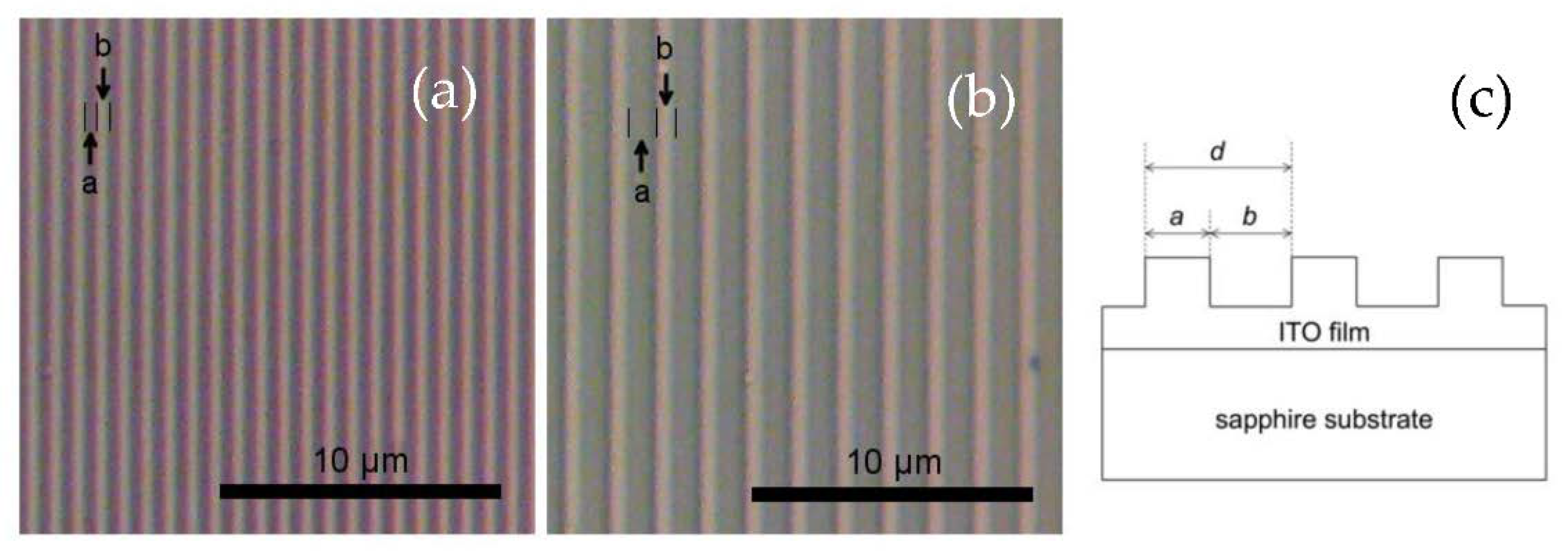
2. Materials and Methods

We prepared ITO films having grating structure with different pitches. The samples were prepared by following procedures. At first, ITO films were deposited on sapphire substrate at 300 °C by RF sputtering. We used the ITO ceramics target which contains [Sn] of 10%. The film thickness was roughly estimated at 700 nm. And then, the electronic properties were measured by Hall measurement, and the sample has the electron density and the mobility of 7.5 × 1020 cm−3 and 21 cm2V−1s−1, respectively. Second, the diffraction grating structures were fabricated by focused ion beam (FIB) technique. We prepared several grating structures with different pitches on the surface of one ITO film, and the grating pitches d were varied from 0.9 to 1.6 µm as a designed value. The micro structure of the grating was observed by optical microscope. And, the optical reflection properties of the sample were evaluated by the micro-optical reflection measurement.

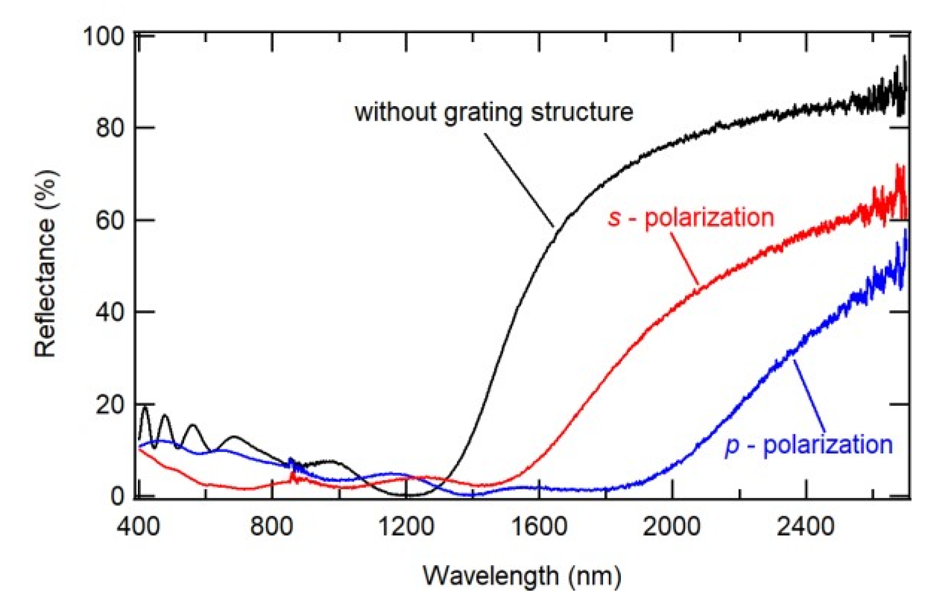
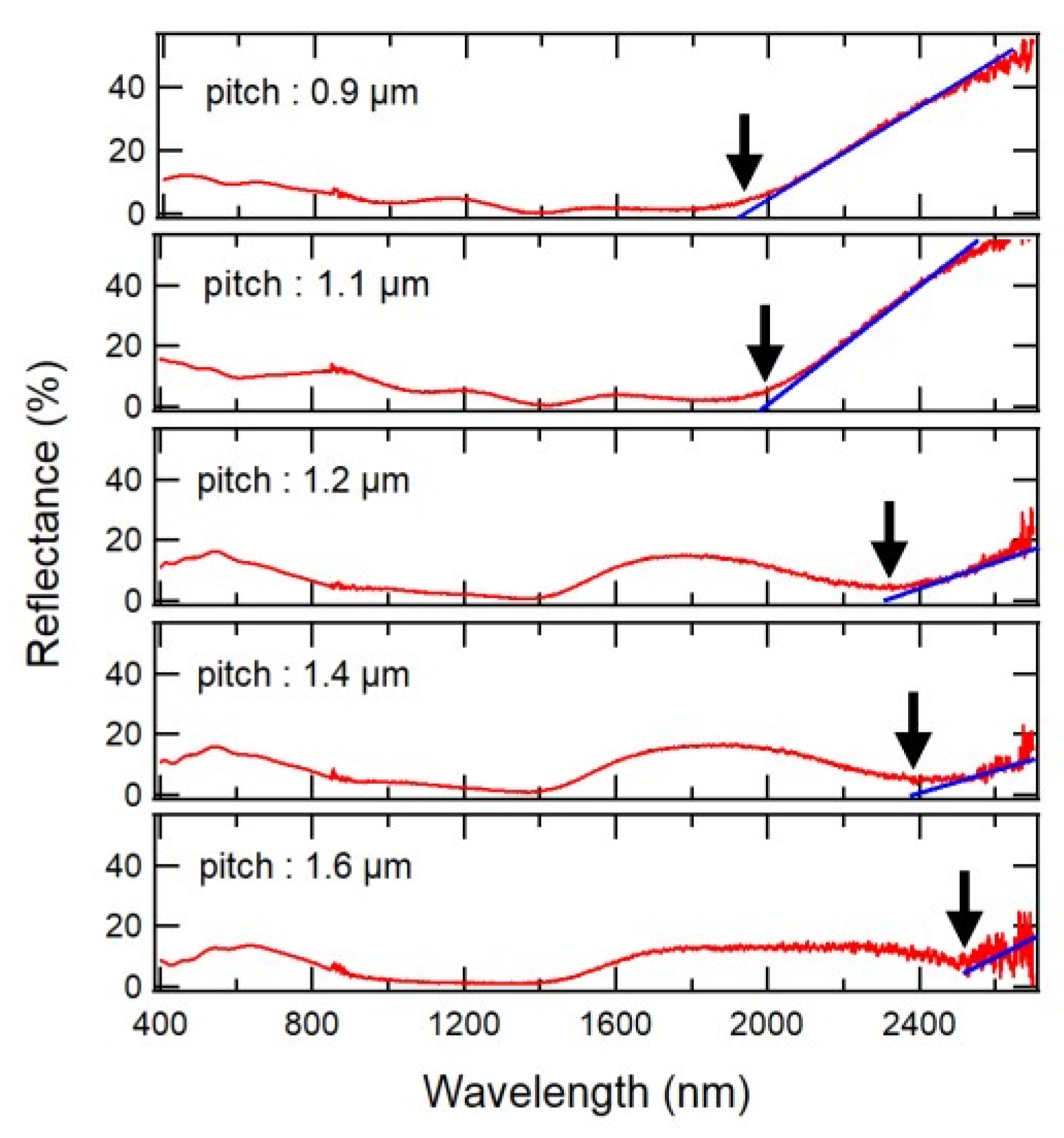
3. Results and Discussion

Figure 1a,b show the optical micrographs of the grating having the pitch “d” of 0.9 and 1.6 µm as a designed value, respectively. And, the schematic diagram of the grating structure is shown in Figure 1c. The characters of “a” and “b” shown in Figure 1a,b correspond to those characters in Figure 1c, and then the grating pitch “d” is given by adding “a” and “b”.
The stripes with definite contrast were observed in Figure 1a,b, and it was confirmed that the dark and bright stripes correspond to the part of “a” and “b”, respectively. The value of “d” were measured by using image processing software (PicMan from WaferMasters, Inc., Dublin, CA, USA). The measured values with standard deviation were summarized at Table 1, and the differences between designed and measured value were also shown in Table 1.
Figure 2 shows the optical reflection spectra for the gratings of 0.9 μm pitch. For comparison, the spectrum taken from the flat surface, without grating structure, was also shown in the figure. The incident light was polarized to the direction of diffraction gratings, and the polarization direction is described as s- and p-polarization. The former means that the direction of electric field of incident light is perpendicular to the direction of grating vector, and the latter means that these directions are parallel. It was clearly observed that the spectrum taken from the flat surface shows the interference patterns in the visible region. And then, the reflectance sharply increases at the wavelength of ~1.4 μm in the spectrum. This feature can be explained as plasma reflection by free electrons in the ITO film, and the mechanism is based on Drude model which often applied to metallic materials. The wavelength of the plasma reflection edge depends on the electronic properties such as electron density, mobility, effective mass and dielectric constant [3,4]. In the spectrum of s-polarization, the plasma reflection edge shifted to longer wavelength side, and the slope also became gentle slightly. Although the shift indicates the decrease in density of free electrons in the film, there are several possibilities regarding the reason. First, the grating structures were fabricated by FIB, in which the processes were carried out by using focused Ga ion beam. Usually, Ga ions become trivalent ion and its oxide Ga2O3 has larger bandgap than that of In2O3. If some Ga ions were incorporated in the ITO film during the fabrication processes, they might form Sn: In2−xGaxO3 alloy, which has larger bandgap energy than ITO, near the surface of grating structure. This causes the increase in activation energy of donors and decrease in the free electron density in Sn: In2−xGaxO3 alloy. At the same time, FIB processes might generate the oxygen vacancies, because the processes were carried out in the high vacuum condition and Ga ions with high energy can be used for fabrication. Above these two factors causes the decrease in electron density [5,6]. Second, the FIB processes might cause some damages such as disorder and defects on the sample surface, and these strongly influence the electric conductivity in ITO film. Especially, the plasma oscillation of the free electron is strongly damped, which appears as a change in slope of the plasma reflection edge on the spectrum. In our case, the slope become gentle slightly, which means the strong damping of the plasma oscillation due to the deterioration of the crystallinity of ITO films. As mentioned above, we consider that the shift and the change in slope of the plasma reflection edge in the spectrum with s-polarization might be caused by both the incorporation of Ga ions and the deterioration of the crystallinity. On the other hand, although the p-polarization spectrum showed same slope on the reflection edge as s-polarization spectrum, the position of the reflection edge showed further shift in the p-polarization spectrum. This is due to the excitation of SPR on the ITO gratings. It has well-known that the excitation of SPR with gratings can be achieved by using p-polarized incident light. The shift can be considered due to the SPR excitation appeared around the wavelength at 1.8 μm. Here, we think about the validity of the SPR excitation wavelength. The SPR with gratings have been well-studied by using metallic gratings, and the SPR wavelength corresponds to the pitch of the grating following the equation below;
𝑘𝑠𝑝 = 𝑘0 sin𝜃 + 𝑛𝑘′
where, ksp and k0 are the wavenumber of the surface plasmon and the incident light, respectively. And, θ is the angle of the incident light with respect to the normal to the diffraction grating plane, and n is the integer. k’ is diffraction grating vector, which is given by 2π/Λ. Λ is the pitch of the grating. As can be seen in the equation, when the p-polarized light was incident perpendicularly to the gratings (θ = 0), ksp has same value as k’ (n = 1). In other word, the SPR wavelength corresponds to the pitch of grating. However, the observed value (~ 1.8 μm) showed the difference from above predicted value (0.9 μm).
Figure 3 shows the optical reflection spectra taken from the other samples (grating 1 to 5). All spectra were observed by using p-polarized incident light, and the SPR wavelength were indicated by arrows in the figure. It was easily confirmed that the SPR wavelength shifted to longer wavelength side as increase in grating pitch. Although this behavior shows qualitatively well correspondence with above theoretical predictions, the values are far from the predicted values. This indicates that the theoretical prediction of SPR wavelength based on metallic grating could not be applied directly to that of TCOs, because TCOs have different electronic band structure from metals. The plasma oscillation in TCO have a relatively large damping constant γ than that in metals. So, in order to analyze the SPR wavelength more accurately in TCO, it is necessary to introduce the influence due to the difference of the electronic band structure from metal.

4. Conclusions

In this study, we prepared ITO film having the diffraction grating structure with micro-meter pitch using FIB technique, and the correlations between the grating pitch and the optical reflection properties were studied. It was confirmed that FIB processes using Ga ion beam had strong influence on the electronic characteristics of ITO film. And, although the excitation of SPR in ITO grating can be achieved by using p-polarized incident light, the observed SPR wavelengths are far from the value which was predicted from the classical theory based on metallic grating. This might be due to the difference of the electronic properties between TCO and metal, and it is necessary to introduce their influences in order to analyze the SPR excitation in TCOs.

References

  1. Morichika, I.; Kusa, F.; Takegami, A.; Sakurai, A.; Ashihara, S. Antenna-Enhanced Nonlinear Infrared Spectroscopy in Reflection Geometry. J. Phys. Chem. C 2017, 121, 11643–11649. [Google Scholar] [CrossRef]
  2. Matsui, H.; Furuta, S.; Tabata, H. Role of electron carriers on local surface plasmon resonances in doped oxide semiconductor nanocrystals. Appl. Phys. Lett. 2014, 104, 211903. [Google Scholar] [CrossRef]
  3. Wolf, N.; Gerstenlauer, D.; Manara, J. Modelling the spectral reflectances of miscellaneous ITO coating by using only the Drude theory. J. Phys. Conf. Ser. 2012, 395, 012064. [Google Scholar] [CrossRef]
  4. Look, D.C.; Leedy, K.D. Optical measurements and mapping in Ga- and Al-doped ZnO and Sn-doped In2O3. Phys. Status Solidi A 2015, 212, 1427–1432. [Google Scholar] [CrossRef]
  5. Choi, J.H.; Kang, S.H.; Oh, H.S.; Yu, T.H.; Sohn, I.S. Design and characterization of Ga-doped indium tin oxide films for pixel electrode in liquid crystal display. Thin Solid Films 2013, 527, 141–146. [Google Scholar] [CrossRef]
  6. Berginc, M.; Campa, A.; Vojisavljevic, K.; Malic, B.; Panjan, P.; Topic, M. Relation between sputtering parameters and optical electrical properties of Ga doped ITO transparent conductive oxide. Energy Procedia 2015, 84, 183–189. [Google Scholar] [CrossRef]
Figure 1. The optical micrographs of the grating with the pitch “d” of 0.9 µm (a) and 1.6 µm (b) as a designed value. The schematic diagram of the grating structure is shown in (c).
Proceedings 02 01034 g001
Figure 2. The reflection spectra taken from the grating with 0.9 µm pitch by using polarized incident light. The spectrum taken from the flat surface without grating structure is also shown for comparison.
Proceedings 02 01034 g002
Figure 3. The reflection spectra taken from the grating with different pitches by using p-polarized incident light. The SPR wavelengths are shown by the arrows.
Proceedings 02 01034 g003
Table 1. The designed and measured values of the grating pitch, and the difference between these values are also indicated. The measured values are shown with standard deviate.
Designed Value Measured Value Difference |ddesigndmeasured|/ddesign
ddesign (μm) dmeasured (μm) Δ (%)
grating 1 0.9 0.84 ± 0.03 6.7
grating 2 1.1 1.05 ± 0.03 4.5
grating 3 1.2 1.25 ± 0.03 4.2
grating 4 1.4 1.36 ± 0.03 2.9
grating 5 1.6 1.67 ± 0.04 4.4
Publisher’s Note: MDPI stays neutral with regard to jurisdictional claims in published maps and institutional affiliations.

