Proceeding Paper

Design and Numerical Evaluation of a Highly Selective CMOS-Compatible Mid-IR Thermal Emitter/Detector Structure Using Optical Tamm-States †

Institute for Microelectronics and Microsensors, Johannes Kepler University Linz, 4040 Linz, Austria
*
Author to whom correspondence should be addressed.
Presented at the Eurosensors 2018 Conference, Graz, Austria, 9–12 September 2018.
Proceedings 2018, 2(13), 1032; https://doi.org/10.3390/proceedings2131032
Published: 16 November 2018
(This article belongs to the Proceedings of EUROSENSORS 2018)

Abstract

:
In this work we propose and evaluate a concept for a selective thermal emitter suitable for monolithic on-chip integration suitable for fabrication by conventional CMOS-compatible processes. The concept is based on our recently presented work on vertical-cavity enhanced resonant thermal emission (VERTE). Here we present the application of this concept to a slab waveguide structure, instead of depositing extended dielectric layers forming a one-dimensional photonic crystal. We optimize the dimension by certain design considerations and genetic- algorithm optimization and demonstrate effective absorbing/emitting properties (depending on different slab heights) of such a low-cost structure by exciting so-called optical Tamm-states on the metal-dielectric interface.

1. Introduction

Recently, the excitation of optical Tamm plasmon-polaritons (TPPs) at the metal-dielectric interface by 1D multilayer stacks was shown to provide highly coherent absorption and emission properties suitable for monolithic integration into optical absorption sensors [1,2,3].
In this work, we expand the concept of one-dimensional (1D) TPP structures to two dimensional slab structures featuring guided slab modes instead of plane waves. The CMOS-compatible geometry includes a silicon slab waveguide suspended on a thin silicon nitride membrane together with air surroundings (see Figure 1b). The refractive index contrast can be created easily by modern CMOS fabrication processes (e.g., deep reactive ion etching). In general, photonic crystal slab designs introduce an additional confinement of light in lateral direction by index guiding feature an incomplete bandgap [4,5]. Here, the slab layers are considered to be infinitely extended out-of-plane (i.e., z-direction, see Figure 1b). The presented TPP structure confines light vertically (y-direction) by index guiding and horizontally (x-direction) by a bandgap structure. The uniformity of the geometry out-of-plane facilitates numerical evaluation (as it does not require 3D simulations) as well as experimental characterization (higher intensities by extended spatial dimension). For 1D simulations the transfer matrix method (TMM) was employed, whereas the two-dimensional structures were characterized by finite-element method simulations with the software package COMSOL Multiphysics 5.3 (both methods in frequency-domain). Four different slab heights (0.75, 1, 1.25 and 1.5 µm) featuring different fundamental resonance modes are considered and optimized for maximum absorption.

2. Design and Methods

Figure 1a shows a conventional VERTE structure featuring silicon in the continuous region preceding the TPP stack (“bandgap structure” + “cavity”) composed of alternating Air/Si layers.
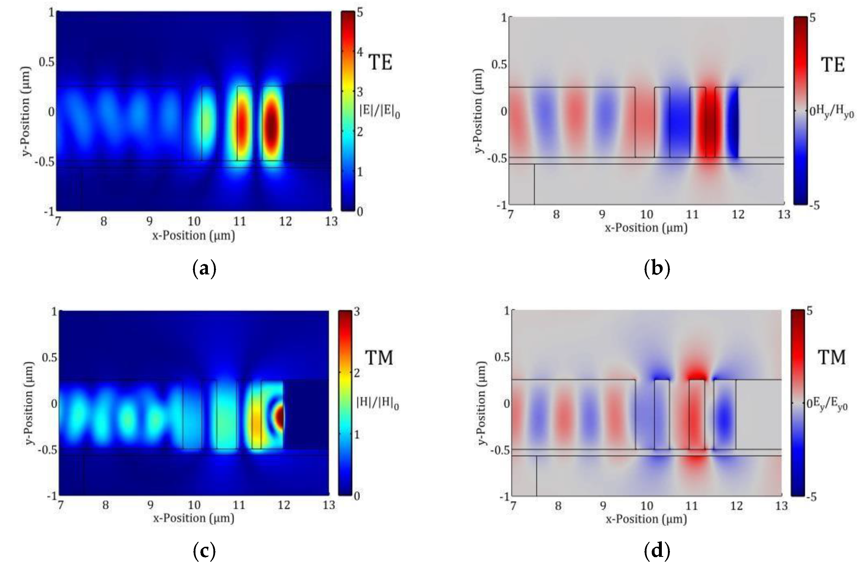
The slab design (Figure 1b) laterally features the same structure including a distributed reflector (DR) as a bandgap structure and a silicon cavity layer with adjusted width (𝑑6), which primarily determines the resonance wavelength. As we focus on the mid-IR region, we set the target resonance wavelength 𝜆 to 4.26 µm (CO2 absorption line). The cavity terminates at a silver interface, which acts as reflective mirror and heat source. Absorbing boundaries were applied at the side walls of the simulation domain (see Figure 1b). Heating of the metal leads to excitation of TPPs at the metal-dielectric interface and results in a monochromatic field enhancement in the cavity (see Figure 2a–d), which couples into the fundamental guided mode of the Si slab. The energy required for heating the metal can be fed from an exterior heat source or by Joule heating. We utilize Kirchhoff’s law and reciprocity by simulating the reciprocal situation of an incident guided mode (propagating in positive x-direction) and evaluate the power absorbed by the silver via Poynting’s theorem. This approach allows efficient simulation of plasmonic emitter structures (see e.g., [1,6,7]).

3. Properties of TPP Structures and Design Considerations

The ultimate goal of the TPP structure design is to avoid radiation losses into the air region. Therefore, some design choices were initially employed before optimizing the structure with a GA algorithm and modifying it for vertical confinement. A first step to minimize the losses is to consider an optical resonance at steady-state featuring a large fraction of the electric field intensities inside the silicon. This facilitates confinement of the cavity resonance by keeping the index guided slab bands away from the light cone [4]. As a result, we set the air gap width 𝑑5 adjacent to the cavity region to 200 nm, which is a feasible limit for a modern deep-reactive-ion etching. Although this represents a significant deviation from a distributed Bragg reflector (DBR), aperiodic configurations are also well known for providing excellent performance as a distributed reflector [2,8]. The lengths of the other air/silicon regions 𝑑1 − 𝑑4 are initially set to quarter wavelength thickness resembling an ordinary DBR. The number of five or six dielectric layers for a VERTE structure together with silver as metal has been proven to be best for optimal performance, as shown in [3]. This configuration now can be optimized using a GA-optimization algorithm with upper and lower bounds on the layer widths. It was set up in a similar way as in Refs. [2,8]. The stack configuration yielding the best results for slab structures together with unity absorptance in the 1D case (see inset of Figure 1a) was used for further optimization for a maximum absorption performance at the target resonance wavelength by carefully modifying the individual widths 𝑑1-𝑑6 (with the exception of 𝑑5) for every slab height 𝑤. An increase of 𝑤 results in an increase of the propagation constant 𝑘𝑥 of the fundamental slab mode. As a result, the horizontal layer widths tend to decrease (especially 𝑑6) for increasing 𝑤. Simultaneously, energy of a slab cavity mode cannot be described by two perpendicular field oscillations (horizontal and vertical). An increasing ratio d 6 w increases the energy contained in such a mode, as the field at the corner regions deviates significantly from a superposition of horizontal and vertical field oscillations. As this increases the resonant incident wavelength (resonance now occurs at lower energies), the dimensions have to be scaled to smaller values for decreasing 𝑤 in order to reach the target resonant wavelength of 4.26 µm.
As a result, both effects (reduction of 𝑘𝑥 and increase of cavity mode energy by mode profile) compensate each other for the most part enabling the utilization of the geometry by slab structures by only slightly modifying the individual widths from the configuration obtained by the GA-optimization (see Table 1).

4. Evaluation and Results

We calculate the power fraction absorbed by the silver by surface integration of the orthogonal Poynting vector component (real part, x-component) along the Si-Ag interface [4,6]. The net power flux (i.e., absorption) into the silver is evaluated as P x TE = 1 2 0 w Re ( E z ( x int , y ) H y * ( x int , y ) )   d y for TE-polarization (𝐸𝑧 only) and as P x TM = 1 2 0 w Re ( E y ( x int , y ) H z * ( x int , y ) )   d y for TM-polarization (𝐻𝑧 only), respectively, where 𝑥int denotes the horizontal position of the Si-Ag interface. Each configuration with different slab height was optimized for a maximum absorption performance at the resonance wavelength at 4.26 µm for TE polarization. Table 1 and Figure 3a show the optimized dimensions for each configuration and the absorbed power fraction they could provide. Increasing 𝑤 from 0.75 to 1.5 µm results in an increased mode confinement (as explained above) and, subsequently, in an increased relative absorption by the silver at resonance A res   TE from 70% to nearly 90%. It is worth mentioning that the high absorption for 𝑤 = 1.5 µm assumes an incoming fundamental slab mode.
Although an essential property of TPP resonator structures is that they are largely independent of polarization (especially for small angles), this is not true for applying this concept to slab structures with incomplete bandgaps. Introducing an index guiding slab fundamentally introduces a symmetry axis along the plane y = w 2 resulting in a subdivision into even and odd modes with respect to the electric field profiles, depending on the polarization of the slab mode. Particularly for TM polarization, the field profile 𝐸𝑥 is odd (i.e., it has a node in the symmetry plane, see Figure 1c). This has significant consequences for the confinement of the fields at resonance, as the odd field in the slab does not couple as efficiently to a cavity mode compared to the case of an even electric field profile (see Figure 3c). As a result, the coupling to radiation modes is much higher and the resonance Q-factor is much worse for TM polarization.
For example, peak at 3.7 µm in Figure 3b (green line) does not only feature a lower maximum absorption, the resonance peak also is much broader indicating greatly enhanced radiation loss. The resonant wavelength is lower for the corresponding TM resonance (characteristic field 𝐸𝑦 can be seen in Figure 2d), reflecting the higher energies of the index guided TM band.

Acknowledgments

This project has been supported by the COMET K1 centre ASSIC Austrian Smart Systems Integration Research Center. The COMET—Competence Centers for Excellent Technologies- Programme is supported by BMVIT, BMWFW and the federal provinces of Carinthia and Styria.

Conflicts of Interest

The authors declare no conflict of interest. The founding sponsors had no role in the design of the study; analyses; in the writing of the manuscript, and in the decision to publish the results.

References

  1. Yang, Z.Y.; Ishii, S.; Yokoyama, T.; Dao, T.D.; Sun, M.G.; Pankin, P.S.; Timofeev, I.V.; Nagao, T.; Chen, K.P. Narrowband wavelength selective thermal emitters by confined tamm plasmon polaritons. ACS Photonics 2017, 4, 2212–2219. [Google Scholar] [CrossRef]
  2. Pühringer, G.; Jakoby, B. Taming parasitic thermal emission by Tamm plasmon polaritons for the mid-infrared. J. Opt. Soc. Am. B 2018, 35, 1490–1503. [Google Scholar] [CrossRef]
  3. Celanovic, I.; Perreault, D.; Kassakian, J. Resonant-cavity enhanced thermal emission. Phys. Rev. B 2005, 72, 2–7. [Google Scholar] [CrossRef]
  4. Joannopoulos, J.J.D.; Johnson, S.; Winn, J.N.J.; Meade, R.R.D. Photonic Crystals: Molding the Flow of Light; Prinston University Press: Princeton, NJ, USA, 2008. [Google Scholar]
  5. Villeneuve, P.R.; Fan, S.; Johnson, S.G.; Joannopoulos, J.D. Three-dimensional photon confimement in photonic crystals of low-dimensional periodicity. IEE Proc. 1998, 145, 384–390. [Google Scholar]
  6. Lipson, M.; Pollock, C. Integrated Photonics; Kluwer Academic Publishers: Norwell, MA, USA, 2003. [Google Scholar]
  7. Pühringer, G.; Jakoby, B. Efficient Vertical-Cavity Mid-IR Thermal Radiation to Silicon-Slab Waveguide Coupling Using a Shallow Blazed Grating. Proceedings 2017, 1, 286. [Google Scholar] [CrossRef]
  8. Granier, C.H.; Afzal, F.O.; Min, C.; Dowling, J.P.; Veronis, G. Optimized aperiodic highly directional narrowband infrared emitters. J. Opt. Soc. Am. B 2014, 31, 1316–1321. [Google Scholar] [CrossRef]
Figure 1. 1-D Simulation domain of the conventional TPP structure for the Transfer-Matrix Method (a) and 2-D FEM simulation domain of the slab TPP structure (b). The inset in (a) shows the absorption performance of the GA optimized stack configuration. The even 𝐻𝑧 profile (upper panel) and the odd 𝐸𝑥 profile of the pure TM slab mode is shown in (c).
Proceedings 02 01032 g001
Figure 2. Resonance profile for the total electric field amplitude |𝐸| (a) and the y-component of the magnetic field 𝐻𝑦 (b) (TE) and 𝑤 = 1.5 µm. The correspondings fields (TM) of |𝐻| and 𝐸𝑦 are shown in (c,d). |𝐸|0,0,|𝐻|0,𝐸𝑦0 denote the incident wave field amplitude.
Proceedings 02 01032 g002
Figure 3. Absorbed fraction of incoming light by Ag of the slab TPP structure for TE (a) and TM (b) polarization. The broad peaks around 3.5 µm featured by the green, black and blue lines and the peak at 3 µm of the red line in (b) correspond to the TM-resonance featuring a similar electric field profile as in the TE case. (c) Odd 𝐸𝑥 mode profile at the TM resonance (λ = 3.7 µm, 𝑤 = 1.5 µm).
Proceedings 02 01032 g003
Table 1. Widths and absorption for the obtained optimized configurations and featuring different slab heights 𝑤 from 0.75 to 1.5 µm. 𝑤 = ∞ corresponds to the 1D VERTE structure.
𝒘 (µm) 𝒅𝟏 𝒅𝟐 𝒅𝟑 𝒅𝟒 𝒅𝟓 𝒅𝟔 A res   TE
1 0.40 0.33 0.410.350.15 0.48 100%
1.5 0.42 0.33 0.44 0.35 0.2 0.49 90%
1.25 0.44 0.34 0.45 0.36 0.2 0.50 84%
1 0.42 0.35 0.44 0.37 0.2 0.52 80%
0.75 0.45 0.37 0.46 0.39 0.2 0.54 70%
1 1D VERTE structure obtained directly from GA-optimization (incident plane wave, see Figure 1a).
Publisher’s Note: MDPI stays neutral with regard to jurisdictional claims in published maps and institutional affiliations.