Proceeding Paper

On-Glass Optoelectronic Platform for On-Chip Detection of DNA †

by
Domenico Caputo
1,*,
Francesca Costantini
2,3,
Nicola Lovecchio
1,
Marco Nardecchia
1,3,
Augusto Nascetti
3 and
Giampiero de Cesare
1
1
Department of Information Engineering, Electronics and Telecommunications, Sapienza University of Rome, 00184 Rome, Italy
2
Department of Chemistry, Sapienza University of Rome, 00185 Rome, Italy
3
School of Aerospace Engineering, Sapienza University of Rome, 00138 Rome, Italy
*
Author to whom correspondence should be addressed.
Presented at the Eurosensors 2018 Conference, Graz, Austria, 9–12 September 2018.
Proceedings 2018, 2(13), 1014; https://doi.org/10.3390/proceedings2131014
Published: 3 December 2018
(This article belongs to the Proceedings of EUROSENSORS 2018)

Abstract

:
Lab-on-chip are analytical systems which, compared to traditional methods, offer significant reduction of sample, reagent, energy consumption and waste production. Within this framework, we report on the development and testing of an optoelectronic platform suitable for the on-chip detection of fluorescent molecules. The platform combines on a single glass substrate hydrogenated amorphous silicon photosensors and a long pass interferential filter. The design of the optoelectronic components has been carried out taking into account the spectral properties of the selected fluorescent molecule. We have chosen the [Ru(phen)2(dppz)]2+ which exhibits a high fluorescence when it is complexed with nucleic acids in double helix. The on-glass optoelectronic platform, coupled with a microfluidic network, has been tested in detection of double-stranded DNA (dsDNA) reaching a detection limit as low as 10 ng/µL.

1. Introduction

Detection of deoxyribonucleic acid (DNA) has always received a lot of attention in different and important fields such as genetic research [1], food safety [2], forensic [3] and so on. At the same time, in the last years, lab-on-chip systems have known a great development due to the significant reduction of sample, reagent, energy consumption and waste production that they offer with respect to the traditional methods. Detection systems based on electrochemical [4] mechanical [5] and optical [6] methods have been developed. Among the optical techniques, mostly of those used for DNA detection are based on the detection of fluorescence. This is usually determined by fluorophores/fluorochromes intercalated into the target DNA molecules [7].
In this paper, we report the technological development of an on-glass optoelectronic platform based on thin film technologies for fluorescence detection. The proposed platform is a very compact system, because reduces to a few hundred of microns the distance between the fluorescence source and the photosensor. This characteristic leads to a strong decrease of optical losses due to light diffusion and to an improvement of limit of detection and sensitivity of the system.

2. Materials and Methods

The optoelectronic devices have been fabricated through standard microelectronic thin film technologies such as photolithography, metal, semiconductor and oxide deposition and etching. The platform assembly foresees at first the photosensor fabrication and subsequently the filter deposition.

2.1. a-Si:H Photosensor Fabrication

The a-Si:H sensors are n-type doped/intrinsic/p-type doped stacked structures fabricated through a five-mask procedure described in [8]. In particular, the photodiodes have been deposited by Plasma Enhanced Chemical Vapor Deposition at temperature below 200 °C. The thickness of the n, i, and p regions are 50, 350 and 10 nm, respectively.

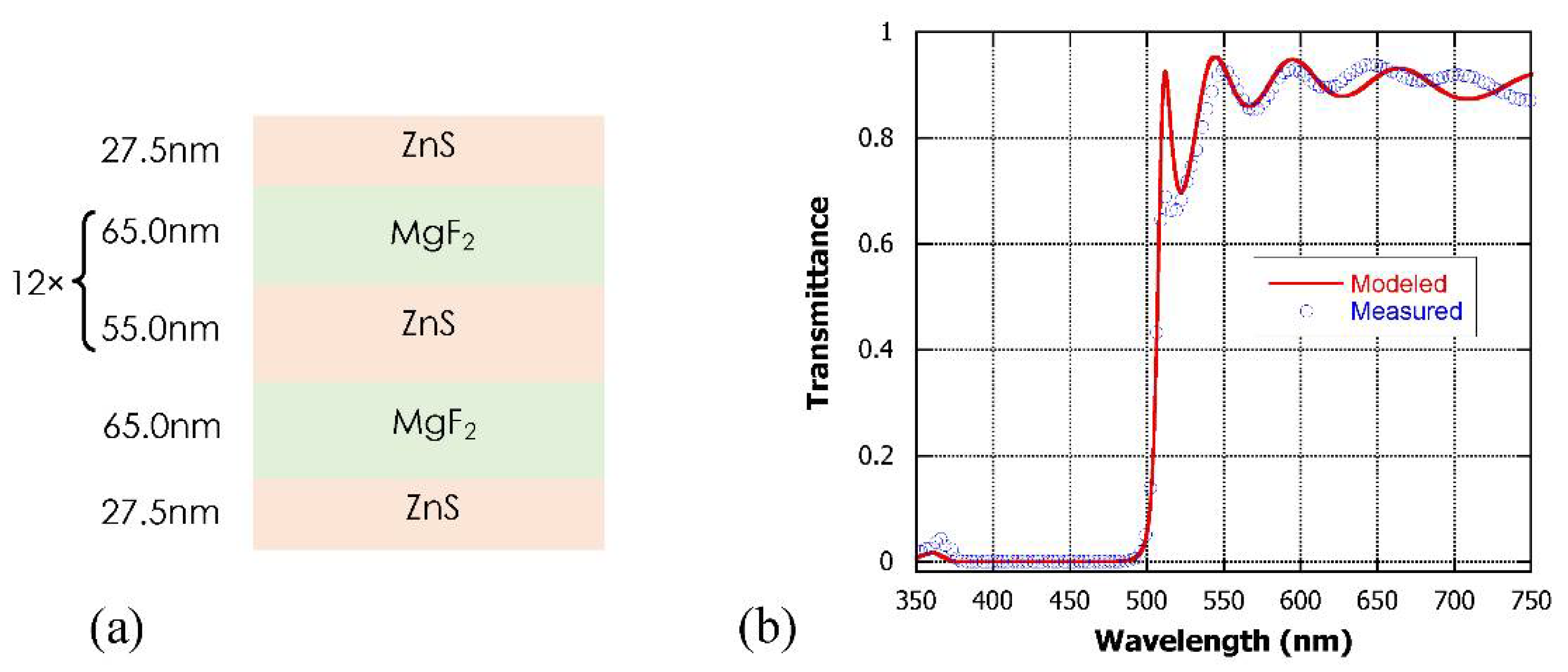
2.2. Filter Fabrication

The filter is a long-pass interferential constituted by alternating layers of zinc sulfide (ZnS) and magnesium fluoride (MgF2) deposited directly over the a-Si:H diodes. Its structure is reported in Figure 1a. In order to avoid degradation of the optoelectronic performances of the previously deposited a-Si:H photodiodes, the filter has been deposited at room temperature by Electron Beam Physical Vapor Deposition without any patterning process.

2.3. Microfluidic Network Fabrication

The microfluidic network, constituted by a 40 mm-long, 1 mm-wide and 50 µm-high linear channel, is made in polydimethylsiloxane (PDMS). The one used in this work is the Sylgard 184 (Dow Corning, Midland, MI, USA), constituted by a base and a curing agent. The microfluidic chip has been fabricated by pouring a mixture of the PDMS linear polymer and the crosslinker over a mold deposited on a silicon wafer. After curing (at 60 °C for 2 h 30 min), the PDMS has been peeled from the mold and bonded to the glass substrate using the transfer bonding technique with PDMS as adhesive [9].

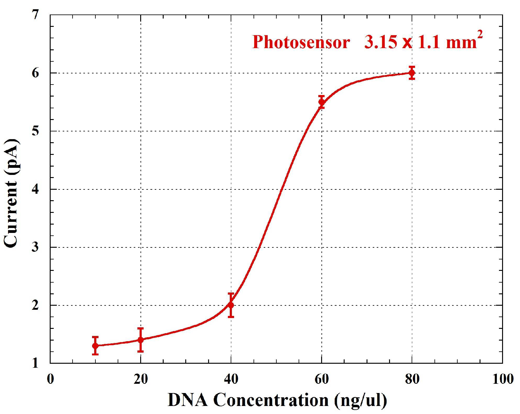
3. Results and Discussion

As reported in Figure 2, the platform combines on a single glass substrate a-Si:H photosensors [10] and a long pass interferential filter [11]. The operation principle of the system is based on the excitation of a fluorescent dye complexed with the double-stranded DNA (dsDNA) molecules through a suitable radiation source. The filter reflects the excitation radiation and transmit only the re-emitted light, which is detected by the photosensors and monitored as output current signal.
The design of both photosensors and filter depends on the optical properties of the selected fluorescent dye. In our work, we have chosen the ruthenium complex [Ru(phen)2(dppz)]2+ which exhibits a high fluorescence when it is complexed with nucleic acids in double helix. Specifically, the absorption spectrum of the [Ru(phen)2(dppz)]2+-dsDNA complex is centered at 400 nm, while its fluorescence shows a strong emission with a peak around 610 nm [12]. Taking into account these characteristics, the filter has been designed as an interferential structure by using XOP [13].
We have preliminarily measured the performances of the interferential filter and the photosensors. The experimental data of transmittance of the filter deposited on a plain glass substrate are reported in Figure 1b. We observe a long-pass behavior with a cut-off wavelength (50% of transmittance) at 510 nm and a very good agreement between theory and experiment. Furthermore, from the raw data we derive that the ratio between the transmittance at 610 nm and 400 nm is equal to 105 indication of a very good rejection of the excitation source.
From the experimental characterization of the photosensors before and after the filter deposition, we have found that while the spectral response remains almost unchanged for wavelength longer than 550 nm, it presents a sharp decrease at wavelengths below 530 nm. Specifically, we found that:
Q Y B ( 400   nm ) Q Y A ( 450   nm ) = 400 ,  
where QYB and QYA are the quantum efficiency before and after the filter deposition, respectively.
Testing of the system in detection has been performed by coupling the optoelectronic platform to the microfluidic network. The micro-channels have been aligned with the a-Si:H photosensors and filled with solutions at different dsDNA concentrations and a fixed concentration of ruthenium complex equal to 6 × 10⁻⁵ M. Results are reported in Figure 3. Data demonstrate the successful detection of dsDNA with a detection limit of 10 ng/µL.

4. Conclusions

We have presented an integrated optoelectronic platform designed to detect fluorescent molecule. In particular, a-Si:H photosensors and a thin film interferential filter have been fabricated on a single glass substrate, by using thin film microelectronic technologies. The system has been tested by coupling the optoelectronic platform to a PDMS microfluidic network, filled with solutions at different dsDNA concentrations and a fixed concentration of [Ru(phen)2(dppz)]2+. A detection limit of 10 ng/µL has been achieved, suggesting that the proposed system is effective for application in the real-time monitoring of DNA amplification.

Author Contributions

D.C., A.N., G.C. designed the optoelectronic platform, F.C. conceived and designed the DNA experiments; M.N., D.C. and G.C. and fabricated the optoelectronic platform, F.C. and N.L. performed the experiments on DNA; all authors analyzed the data; D.C. wrote the paper.

Acknowledgments

Authors thank the Italian Space Agency through the project PLEIADES and the MIUR through the University Research Project 2017 (prot. RG11715C8213BD81).

Conflicts of Interest

The authors declare no conflict of interest.

References

  1. Schena, M. Microarray Analysis; John Wiley & Sons: Hoboken, NJ, USA, 2003. [Google Scholar]
  2. Munster, V.; Wallensten, A.; Olsen, B.; Rimmelzwaan, G.F.; Osterhaus, A.D.M.E.; Fouchier, R.A.M. Influenza A Virus Surveillance in Wild Birds. In Avian Influenza: Prevention and Control; Schrijver, R.S., Koch, G., Eds.; Springer: Dordrecht, The Netherlands, 2005; Chapter 4; pp. 25–30. [Google Scholar]
  3. Butler, J.M. Advanced Topics in Forensic DNA Typing: Methodology; Academic Press: Cambridge, MA, USA, 2011. [Google Scholar]
  4. Wongkaew, N.; He, P.; Kurth, V.; Surareungchai, W.; Baemner, A.J. Multi-channel PMMA microfluidic biosensor with integrated IDUAs for electrochemical detection. Anal. Bioanal. Chem. 2013, 405, 5965–5974. [Google Scholar] [CrossRef]
  5. Waggoner, P.S.; Craighead, H.G. Micro- and nanomechanical sensors for environmental, chemical, and biological detection. Lab Chip 2007, 7, 1238–1255. [Google Scholar] [CrossRef]
  6. Pires, N.M.M.; Dong, T.; Hanke, U.; Hoivik, N. Recent Developments in Optical Detection Technologies in Lab-on-a-Chip Devices for Biosensing Applications. Sensors 2014, 14, 15458–15479. [Google Scholar] [CrossRef] [PubMed]
  7. Bruijns, B.B.; Tiggelaar, R.M.; Gardeniers, J.G. Fluorescent cyanine dyes for the quantification of low amounts of dsDNA. Anal. Biochem. 2016, 511, 74–79. [Google Scholar] [CrossRef] [PubMed]
  8. Petrucci, G.; Caputo, D.; Lovecchio, N.; Costantini, F.; Legnini, I.; Bozzoni, I.; Nascetti, A.; de Cesare, G. Multifunctional system-on-glass for Lab-on-chip applications. Biosens. Bioelectron. 2017, 93, 315–321. [Google Scholar] [CrossRef] [PubMed]
  9. Satyanarayana, S.; Karnik, R.N.A.; Majumdar, A. Stamp-and-stick room-temperature bonding technique for microdevices. J. Microelectromechanical Syst. 2005, 14, 392–399. [Google Scholar] [CrossRef]
  10. Costantini, F.; Sberna, C.; Petrucci, G.; Reverberi, M.; Domenici, F.; Fanelli, C.; Manetti, C.; de Cesare, G.; Derosa, M.; Nascetti, A.; et al. Aptamer-based sandwich assay for on chip detection of Ochratoxin A by an array of amorphous silicon photosensors. Sens. Actuators B Chem. 2016, 230, 31–39. [Google Scholar] [CrossRef]
  11. Caputo, D.; Costantini, F.; Lovecchio, N.; Viri, V.; Tucci, M.; Mangiapane, P.; Ruggi, A.; Petrucci, G.A.; Nascetti, A.G.; de Cesare, G. Highly miniaturized system for on-chip detection of DNA. In Proceedings of the 20th International Conference on Miniaturized Systems for Chemistry and Life Sciences, Dublin, Ireland, 9–13 October 2016; pp. 1234–1235. [Google Scholar]
  12. Jiang, Y.; Fang, X.; Bai, C. Signaling aptamer/protein binding by a molecular light switch complex. Anal. Chem. 2004, 76, 5230–5235. [Google Scholar] [CrossRef] [PubMed]
  13. Available online: http://www.esrf.eu/Instrumentation/software/data-analysis/xop2.4 (accessed on 21 September 2017).
Figure 1. (a) Cross section of the interferential filter structure. (b) Modeled and measured transmittance of the filter deposited on a plain glass substrate.
Proceedings 02 01014 g001
Figure 2. Schematic cross section of the structure for the on-chip detection of DNA. The thicknesses of the interferential filter is a few tens of microns. The thickness of each glass is 1 mm.
Proceedings 02 01014 g002
Figure 3. Sensor photocurrents as a function of the DNA concentration in the solution inside the microfluidic channel. Concentration of ruthenium complex is 6 × 10⁻⁵ M. Symbols and error bars represent the averaged values and standard deviations over three independent measurements, respectively.
Proceedings 02 01014 g003
Publisher’s Note: MDPI stays neutral with regard to jurisdictional claims in published maps and institutional affiliations.

