Fabrication of Planar Copper Microcoils for Telemetric Orthodontic Applications †

Abstract
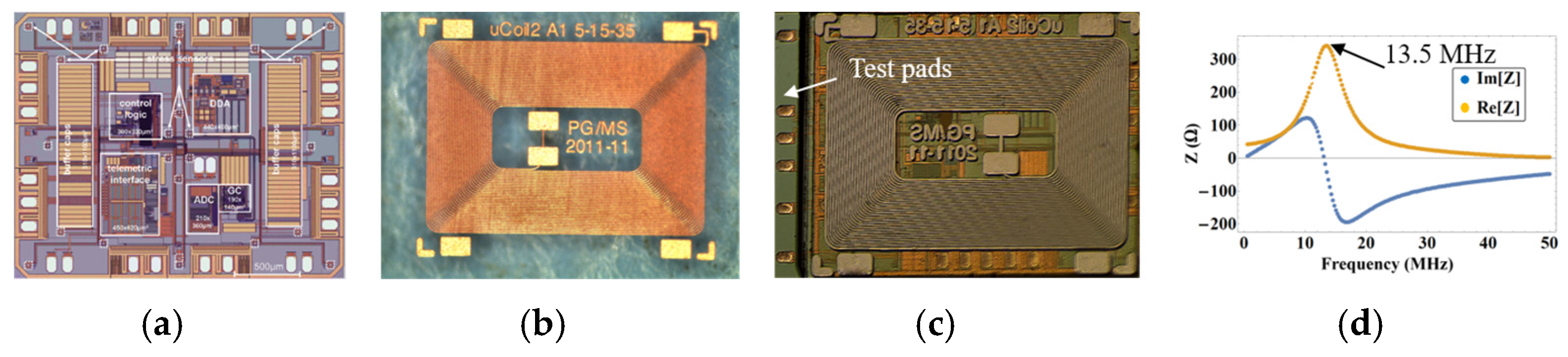
:1. Introduction
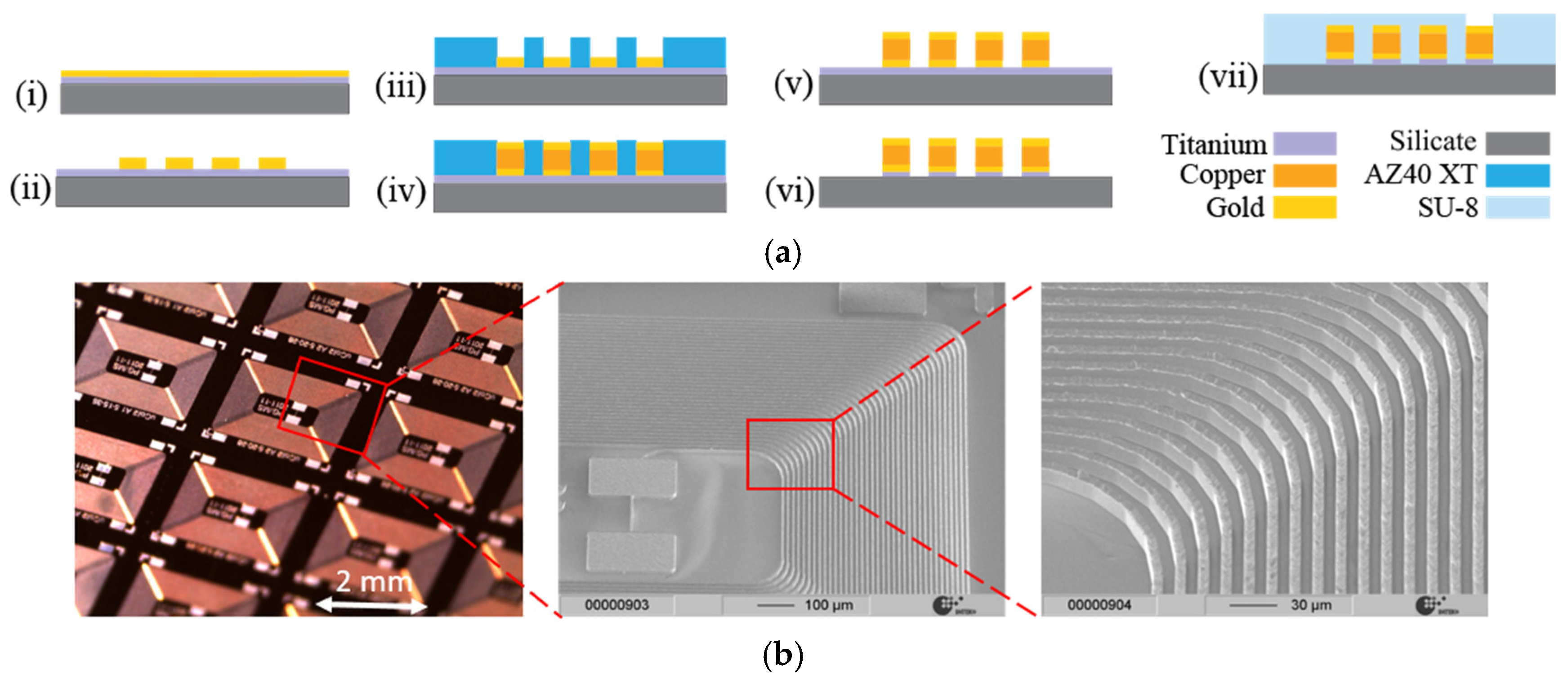
2. Microcoil Fabrication
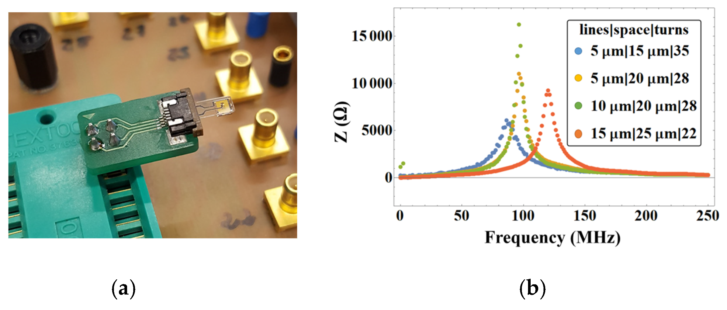
3. Electrical Characterization
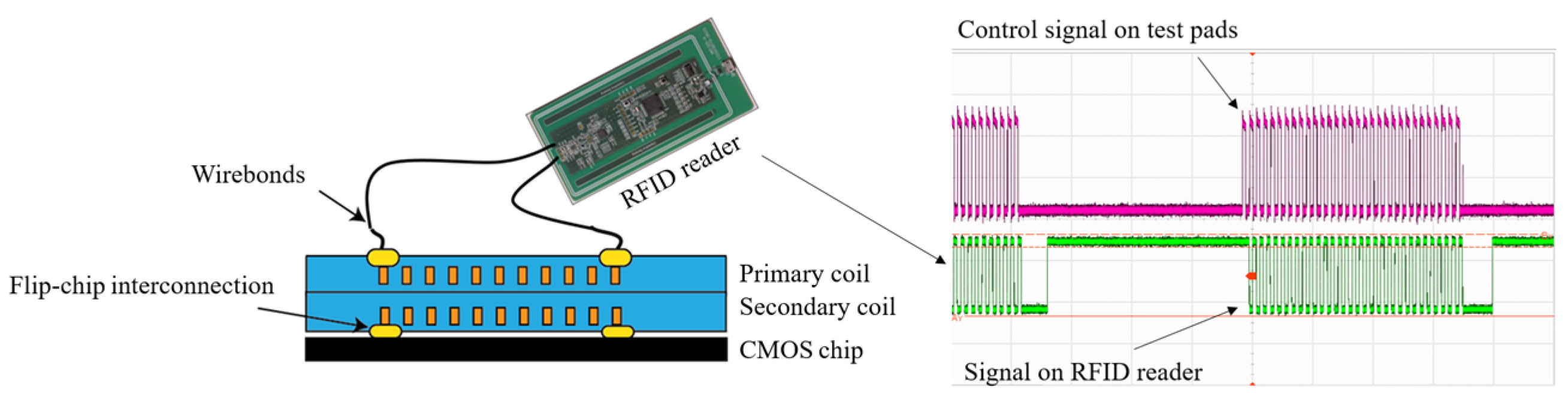
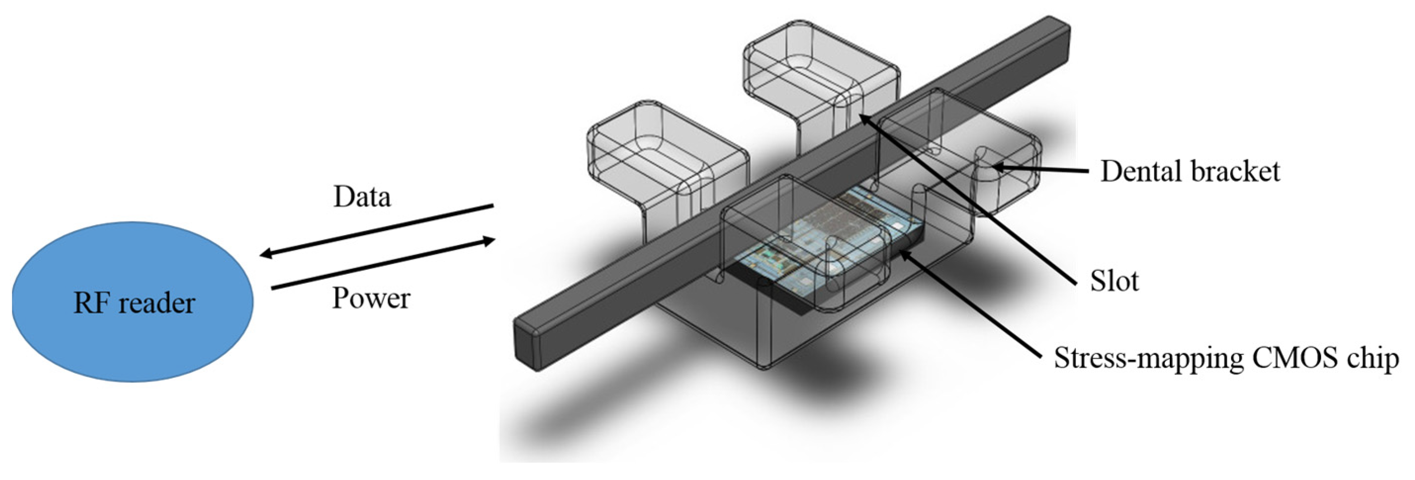
4. System Assembly and Telemetric Link
5. Conclusions
Acknowledgments
Conflicts of Interest
References
- Kuhl, M.; Gieschke, P.; Rossbach, D. A telemetric stress-mapping CMOS chip with 24 FET-based stress sensors for smart orthodontic brackets. In Proceedings of the 2011 IEEE International Solid-State Circuits Conference Digest of Technical Papers (ISSCC), San Francisco, CA, USA, 20–24 February 2011; pp. 108–110. [Google Scholar]
- Bartholomeyczik, J. Advanced CMOS-Based Stress Sensing. Ph.D. Thesis, Department of Microsystems Engineering (IMTEK), University of Freiburg, Freiburg im Breisgau, Germany, 30 April 2006. [Google Scholar]
- Moulin, J.; Woytasik, M.; Martincic, E.; Dufour-Gergam, E. Copper planar microcoils applied to magnetic actuation. In Proceedings of the DTIP; HAL: Stresa, Lago Maggiore, Italy, 2007; hal-00257693; pp. 225–229. [Google Scholar]
- Neagu, C.R.; Jansen, H.V.; Smith, A.; Gardeniers, J.G.E.; Elwenspoek, M.C. Characterization of a planar microcoil for implantable microsystems. Sens. Actuators A Phys. 1997, 62, 599–611. [Google Scholar] [CrossRef]
- Fastfieldsolvers. Available online: http://www.fastfieldsolvers.com (accessed on 28 June 2017).


| Lines | Space | Turns | Measurement | Simulation |
|---|---|---|
| 5 μm | 15 μm | 35 | 2.09 μH | 30 Ω | 1.9 pF | 3.3 μH | 38 Ω | 0.29 pF |
| 5 μm | 20 μm | 28 | 1.58 μH | 23 Ω | 1.9 pF | 2.0 μH | 30 Ω | 0.29 pF |
| 10 μm | 20 μm | 28 | 1.42 μH | 14 Ω | 1.6 pF | 2.0 μH | 15 Ω | 0.29 pF |
| 15 μm | 25 μm | 22 | 1.03 μH | 7 Ω | 1.7 pF | 1.3 μH | 8 Ω | 0.29 pF |
Publisher’s Note: MDPI stays neutral with regard to jurisdictional claims in published maps and institutional affiliations. |
© 2017 by the authors. Licensee MDPI, Basel, Switzerland. This article is an open access article distributed under the terms and conditions of the Creative Commons Attribution (CC BY) license (https://creativecommons.org/licenses/by/4.0/).
Share and Cite
Hafner, J.; Kuhl, M.; Schwaerzle, M.; Hehn, T.; Rossbach, D.; Paul, O. Fabrication of Planar Copper Microcoils for Telemetric Orthodontic Applications. Proceedings 2017, 1, 571. https://doi.org/10.3390/proceedings1040571
Hafner J, Kuhl M, Schwaerzle M, Hehn T, Rossbach D, Paul O. Fabrication of Planar Copper Microcoils for Telemetric Orthodontic Applications. Proceedings. 2017; 1(4):571. https://doi.org/10.3390/proceedings1040571
Chicago/Turabian StyleHafner, Julian, Matthias Kuhl, Michael Schwaerzle, Thorsten Hehn, Daniel Rossbach, and Oliver Paul. 2017. "Fabrication of Planar Copper Microcoils for Telemetric Orthodontic Applications" Proceedings 1, no. 4: 571. https://doi.org/10.3390/proceedings1040571
APA StyleHafner, J., Kuhl, M., Schwaerzle, M., Hehn, T., Rossbach, D., & Paul, O. (2017). Fabrication of Planar Copper Microcoils for Telemetric Orthodontic Applications. Proceedings, 1(4), 571. https://doi.org/10.3390/proceedings1040571