Abstract
A piezo resistive, phase locked loop (PLL) controlled micro tactile measurement system for contact resonance spectroscopy (CRS) at high-aspect-ratio geometries was developed and characterised. Therefore, a piezo resistive silicon cantilever with a silicon tip at its free end was brought into contact with a sample surface and excited into resonance by a piezo actuator. The resonance frequency of the contacted cantilever was tracked by a homemade closed-loop PLL circuit. Different materials and layer thicknesses of photo resist (PR) on silicon were used to validate the system. To optimise the sensitivity and efficiency of the measurement system, amplitude and phase of the cantilever in surface contact were analysed under different contact forces and excitation amplitudes.
1. Introduction
Micro-boreholes are used for ventilating, filtering or injecting applications. Due to their ever-increasing requirements in precision and long-term stability, the demands for the drilling also increase. Gases or fluids flowing inside a hole, interact with the sidewalls and this can quickly lead to abrasions or deposits which alter the specifications of the concerned system. In the case of injection nozzles in motor vehicles, for example, fuel deposits lead to efficiency losses and higher exhaust gas values [1]. To analyse the wear process of spray holes with a diameter of around 100 µm, a non-destructive sensor is needed. Direct imaging of the sidewalls using, e.g., scanning electron microscopy (SEM) analysis, however, needs destructive sample preparation [2]. Recently, we described a tactile piezo resistive cantilever sensor for non-destructive form and roughness measurements of high-aspect-ratio surfaces [3]. Subsequently, we extended the applicability of this probe by an additional operating mode, i.e., contact resonance spectroscopy (CRS) [4], which is well-established for material and layer analysis using atomic force microscopy (AFM) [5,6]. Cantilever tip radius, surface roughness and material specific parameters like the Young's modulus, have an effect on the resonant frequency of the cantilever being in contact with a sample. In this paper the novel measurements setup and its operating principle is described in detail as well as its performance for probing relevant model artefacts, e.g., lithographically patterned photo resist layers on silicon.
2. Measurements Setup and Principle
The measurement setup of the micro tactile sensor and a schematic description for CRS is shown in Figure 1a,b, respectively. We used a piezo positioning table PI P-518.ZCD (Physik Instrumente (PI) GmbH & Co. KG) controlled by a LabView program to adjust the contact force in z-direction. For automatic scanning measurements in x-direction we additionally employed a second positioning table (PI P-621.1CD). With this setup, we are able to scan surfaces over a range of 100 µm. During a CRS measurement the cantilever is forced into resonance, while the resonance frequency is tracked by a homemade PLL circuit. Probing of thin layers of different thicknesses on a thick substrate lead to a resonance frequency shift, which is determined by the stiffness of the cantilever tip-sample contact k*. k* can be calculated by Equation (1) [5]:
where R is the radius of the tip, Ec, Es, νc, and νs are the Young’s moduli and the Poisson ratios of the cantilever and the sample, respectively. F0 is the external force applied to the tip-surface contact, kc and fn are the spring constant and the resonance frequency of the tip-supporting cantilever, respectively.
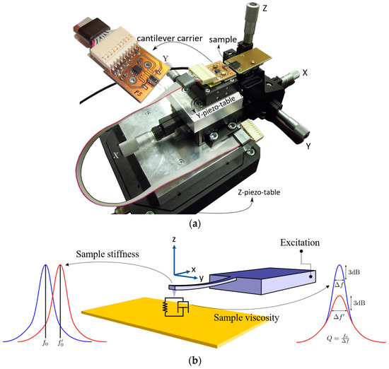
Figure 1.
(a) Measurement setup and (b) schematic description of CRS.
Different materials and photo-resist (PR) layer thicknesses between 0.9 µm and 1.65 µm on a silicon wafer were measured. In automated measurement sequences, transitions between material stacks of different effective plate moduli (Es/(1 − νs2)) were analysed.
3. Results
Figure 2 shows the measurement results for different PR layer thicknesses. Two different contact forces (0.40 mN and 0.93 mN) are used. In relation to Equation 1, the resonance frequency of the cantilever decreases with increasing layer thickness, which is explained by the lower stiffness of the cantilever tip-sample contact k* due to the decreasing influence of the substrate on Es (ESi >> EPR). As expected as well, at the higher probing force we find for all layer thicknesses increased resonance frequencies. According to Equation 1 k* (and thus fn) increases with F0. In Figure 3 and Figure 4, scanning measurements at F0 = 0.67 mN over a length in x-direction of 100 µm are shown. We see a very clear distinction between the PR layer transition and the silicon-PR structure in Figure 3 and Figure 4, respectively. We can see a very clear frequency change at the edges of the PR structures. Using Figure 2 as calibration, we can approximate layer thicknesses of ~2.77 µm and ~0.7 µm for the PR and residual resist layers in Figure 3, respectively. The resonance frequency change in Figure 4 allows an unambiguous material distinction.
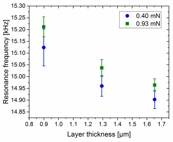
Figure 2.
CRS measurement of different PR-layer thicknesses with two contact-forces (F0) of 0.4 mN and 0.93 mN.
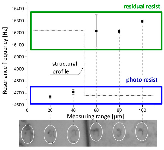
Figure 3.
CRS measurement of a patterned PR-layer in the transition range of 100 µm between the layer and the uncovered substrate area.
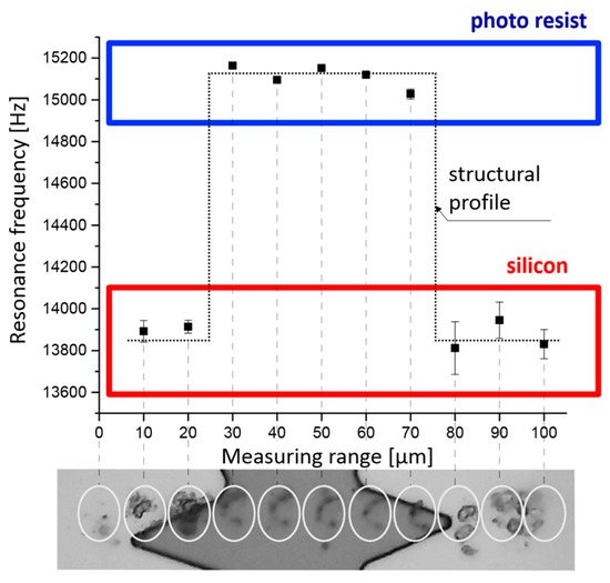
Figure 4.
CRS measurement of a PR-pattern on a silicon wafer over a range of 100 µm.
In the measurements of Figure 4, we see a lower resonance frequency measured on silicon than on PR. This, in relation to Equation (1) unexpected behaviour is caused by the 180° dynamic of the phase detector and the limited bandwidth of the voltage controlled oscillator (fmin = 13,032 Hz, fmax = 16,458 Hz) as illustrated in Figure 5 (grey marked area). Due to this, the PLL detects two 90° transitions, the resonance at ~13.2 kHz and another at ~15.8 kHz as seen in the Bode diagram in Figure 5 for silicon (PR shows a similar behaviour shifted to lower frequencies). Obviously, the PLL locked on the first transition for silicon but at the second transition for PR. This shows a problem of the PLL-circuit which has to be adjusted very accurate to the used cantilever, which can be solved by a dynamic, intelligent PLL-circuit controlled by a micro controller, e.g., using an amplitude comparison.
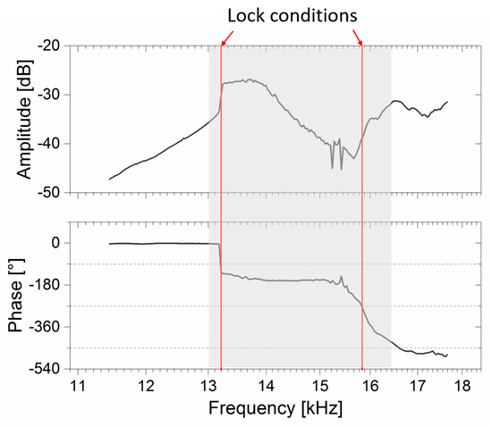
Figure 5.
Bode diagram of a cantilever in contact with a silicon wafer.
4. Conclusions
Experimental measurements of the contact resonance spectroscopy were described. The measurements on silicon and different PR layers show a significant resonance shift that demonstrate the high potential of this measurement method. By using a PLL circuit, the resonance frequency can be tracked in real time. Although some effects are still unanswered, we find a good consistency with the analytic model of CRS. For further clarification and improvements in dynamic and precision of the out-reading electronic, work is ongoing. Besides the frequency profile, a height profile will be able to measured parallel, to combine the CRS with other tactile measurement.
Acknowledgments
The authors thank Karl-Heinz Lachmund for his valuable technical support. Financial support from “Niedersächsisches Vorab”, Germany, through the “Quantum- and Nanometrology (QUANOMET)” initiative with the project NP 2-2 is acknowledged.
Conflicts of Interest
The authors declare no conflict of interest.
References
- Rounthwaite, N.J.; Williams, R.; Mc Givery, C.; Jiang, J.; Giulliani, F.; Britton, B. A Chemical and Morphological Study of Diesel Injector Nozzle Deposits—Insights into their Formation and Growth Mechanisms. SAE Int. J. Fuels Lubr. 2017, 10. [Google Scholar] [CrossRef]
- Henkel, S.; Hardalupas, Y.; Taylor, A.; Conifer, C.; Cracknell, R.; Goh, T.K.; Reinicke, P.-B.; Sens, M.; Rieß, M. Injector Fouling and Its Impact on Engine Emissions and Spray Characteristics in Gasoline Direct Injection Engines. SAE Int. J. Fuels Lubr. 2017, 10. [Google Scholar] [CrossRef]
- Wasisto, H.S.; Doering, L.; Brand, U.; Peiner, E. Ultra-High-Speed Cantilever Tactile Probe For High-Aspect-Ratio Micro Metrology. In Proceedings of the 2015 18th International Conference on Solid-State Sensors, Actuators and Microsystems (TRANSDUCERS), Anchorage, AK, USA, 21–25 June 2015; pp. 1061–1064. [Google Scholar] [CrossRef]
- Zhang, S.; Ding, Y.; Wu, W.; Bertke, M.; Wasisto, H.S.; Doering, L.; Brand, U.; Peiner, E. Direct-reading resonant silicon cantilever for probing of surface deposits. Proc. Eng. 2016, 168, 658–661. [Google Scholar] [CrossRef]
- Rabe, U.; Janser, K.; Arnold, W. Vibrations of free and surface-coupled atomic force microscope cantilevers: Theory and experiment. Rev. Sci. Instrum. 1996, 67, 3281–3293. [Google Scholar] [CrossRef]
- Stan, G.; Solares, S.D. Frequency, amplitude, and phase measurements in contact resonance atomic force microscopies. Bellstein J. Nanotechnol. 2014, 5, 278–288. [Google Scholar] [CrossRef] [PubMed]
Publisher’s Note: MDPI stays neutral with regard to jurisdictional claims in published maps and institutional affiliations. |
© 2017 by the authors. Licensee MDPI, Basel, Switzerland. This article is an open access article distributed under the terms and conditions of the Creative Commons Attribution (CC BY) license (https://creativecommons.org/licenses/by/4.0/).