1. Introduction
Metamaterial-based infrared absorbers are usually fabricated using e-beam lithography, which results in high control over the shape and size of the metallic pattern at the expense of low fabrication throughput [
1]. Such a low fabrication yield hinders the integration of metamaterial structures with MEMS. I-line UV lithography has been recently utilized to alleviate the process integration for the fabrication of the infrared metamaterials and detector arrays by exploiting its batch process capability.
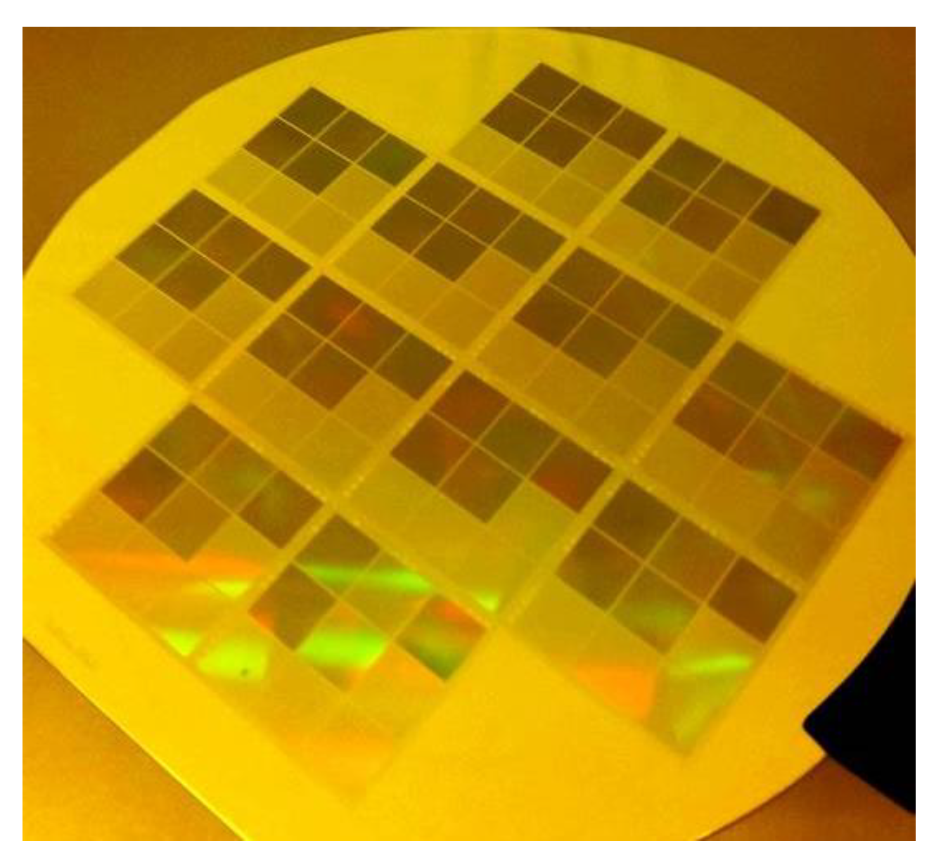
Figure 1 shows a set of metamaterial designs fabricated on the wafer level (4in Si wafer). The dependency of the response of the metamaterial to the shape of the unit-cell enables the fabrication of different designs in a single process. However, the fabrication tolerances involved in the lithography-based process depend on the size and resolution of the pattern and must be assessed to achieve the adequate performance.
While errors in the thickness of the layers have been previously investigated and found to be manageable [
2], surface roughness and uncertainties in the shape and size of the metallic pattern have up to now received less attention. This paper analyzes both surface roughness and shape variations independently and investigates their effects on the performance of the metamaterial absorber.
2. Materials and Methods
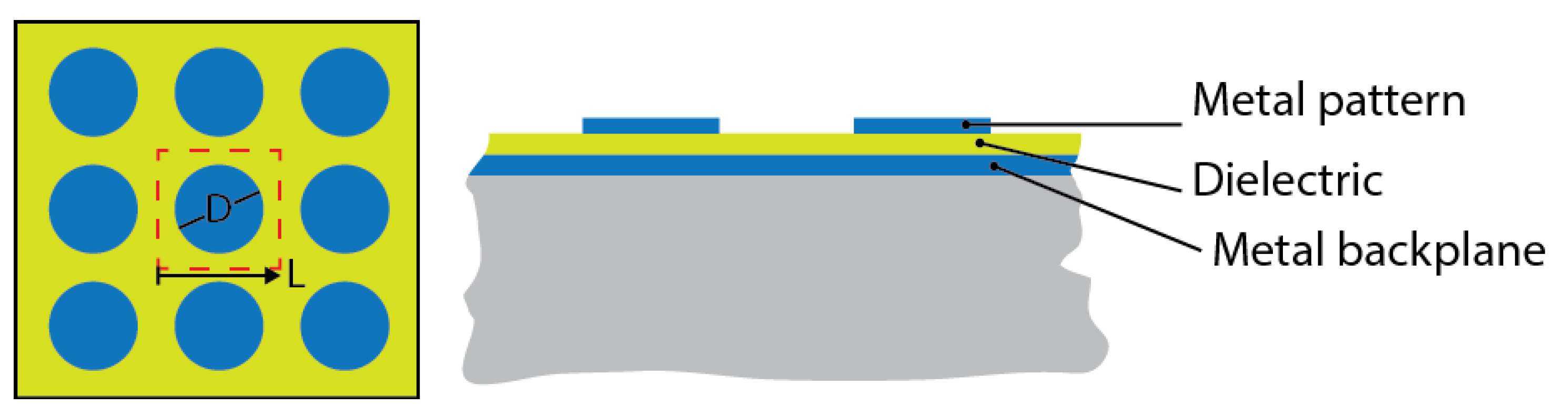
A metamaterial absorber is composed of a metal backplane, a dielectric spacer, and a regular arrangement of a metallic pattern (
Figure 2). The specific arrangement of the metallic pattern and the shape (and size) of the patterns determine the particular response of the metamaterial to the incident electromagnetic wave. Any irregularity or non-uniformity therein (such as absolute dimensions, corner quality, and eccentricity) results in deviations from the expected performance. The overall response of the metamaterial is an averaged effect over a large number of sub-wavelength elements. Therefore, the lateral lithography related defects mainly have a statistical effect on the performance of the structure.
Surface roughness affects the performance of the metamaterial not only due to the scattering of the electromagnetic wave, but more significantly due to the effect of the roughness on the electrical conductivity of the pattern. For a metal layer with a thickness in the order of its electron mean free path (18.9 nm for Aluminum [
3]), the electron-phonon scattering increases with surface roughness and density of grain boundaries, thereby resulting in an increased resistivity in the metal [
4,
5]. Moreover, the increased number of chemical bonds (e.g., native oxide) at the surface of metal increases the imaginary component in the permittivity (high loss angle), thus resulting in increased damping of the surface plasmon resonance [
6]. Finally, the shape of the pattern is affected by the roughness, which further reduces the performance of the metamaterial.
3. Fabrication and Discussion
The effect of the tolerances was tested using different infrared metamaterial absorbers composed of an array of circular aluminum disks. The fabrication process is based on standard UV lithography (ASML PAS 5500/80 wafer stepper), aluminum sputtering, and lift-off. A metamaterial with a disk diameter of 900 nm and a pitch size of 2600 nm results in a sharp spectral absorbance at 3.2 μm with 200 nm full width at half-maximum. Furthermore, tuning the disk diameter from 900 nm to 1100 nm shifts the absorption band from 3.2 μm to 3.8 μm.
For investigating the effect of the roughness, the deposition recipe of the PECVD SiO
2 spacer layer was changed to obtain layers with different surface roughness. The spectral absorbance of the fabricated metamaterials was characterized in reflectance using an FTIR with a reflectance module and compared with the expected response.
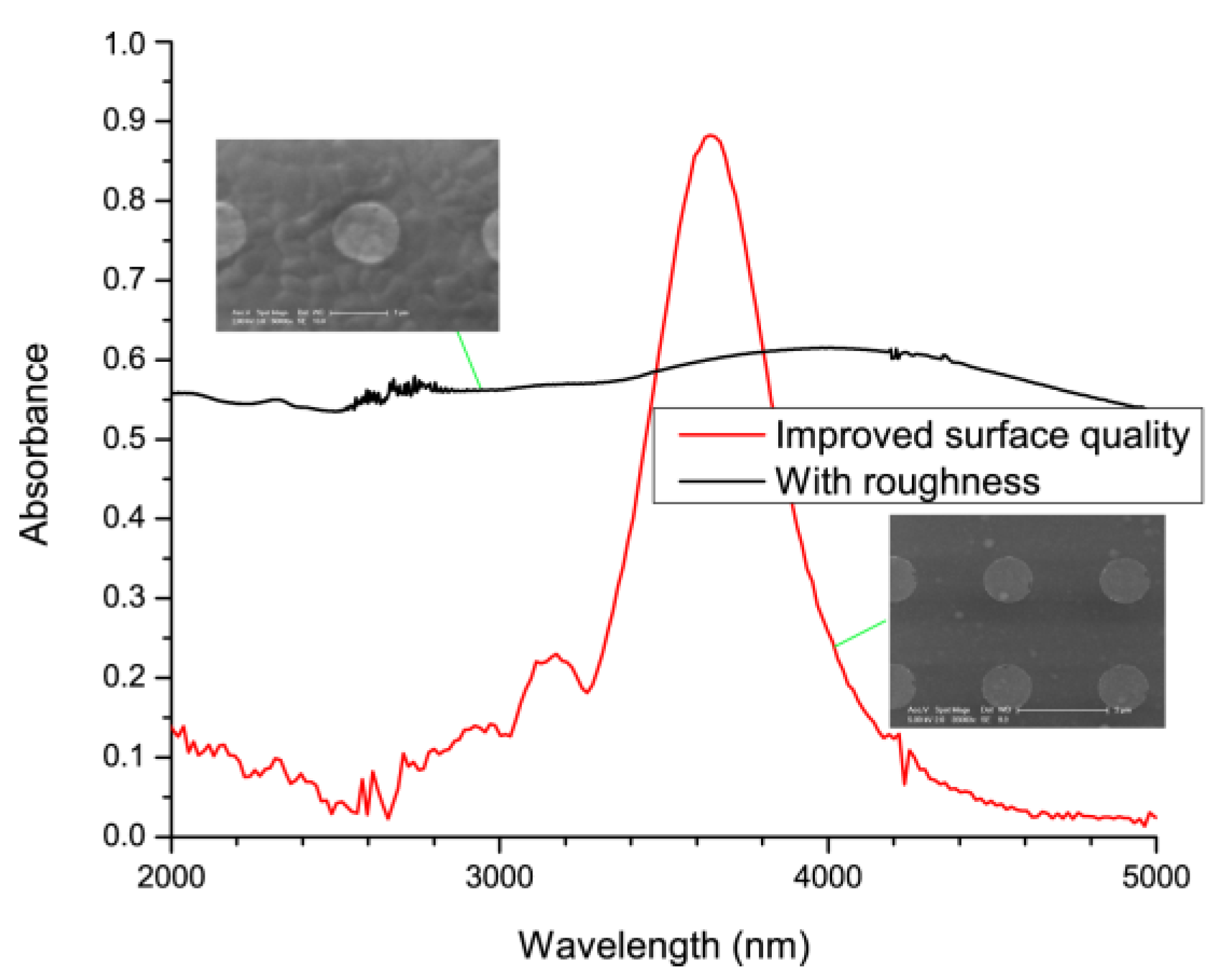
Figure 3 shows the spectral absorbance of the fabricated metamaterials. A high roughness resulted in a near flat absorbance with an amplitude of about 0.5. An improved surface roughness (RMS roughness < 10 nm) was found to highly improve the Q-factor in the resonator.
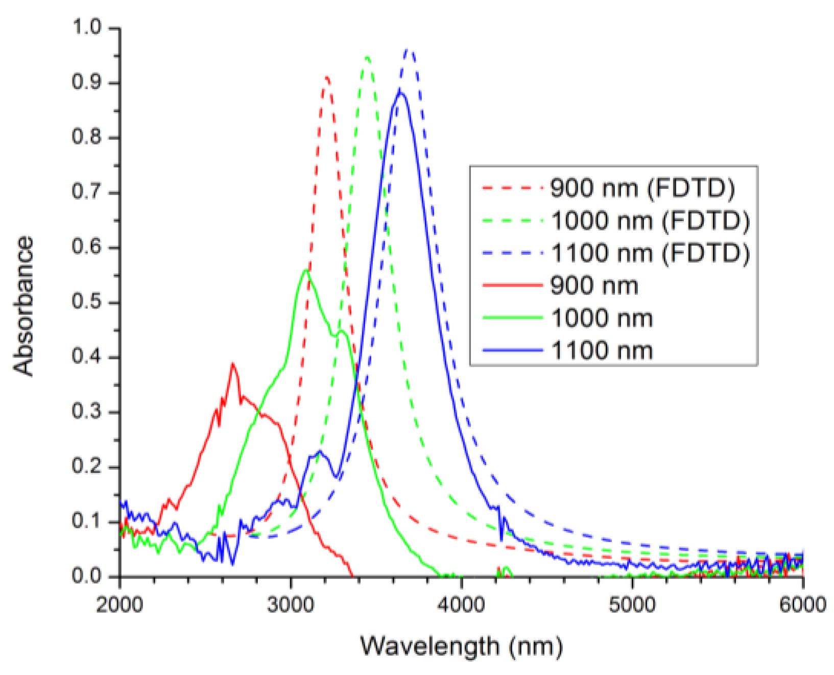
For validating the effect of size variations and eccentricity of the disks, absorbers with 900 nm, 1000 nm, and 1100 nm diameter were fabricated and characterized.
Figure 4 shows the spectral absorbance of the different metamaterial absorbers as compared to the expected value. The fabrication tolerances have resulted in both a peak widening and a shift to shorter wavelengths. Furthermore, the peak intensity is also reduced. As it is expected, the effect of the lithography related errors is higher for designs with a smaller disk diameter.
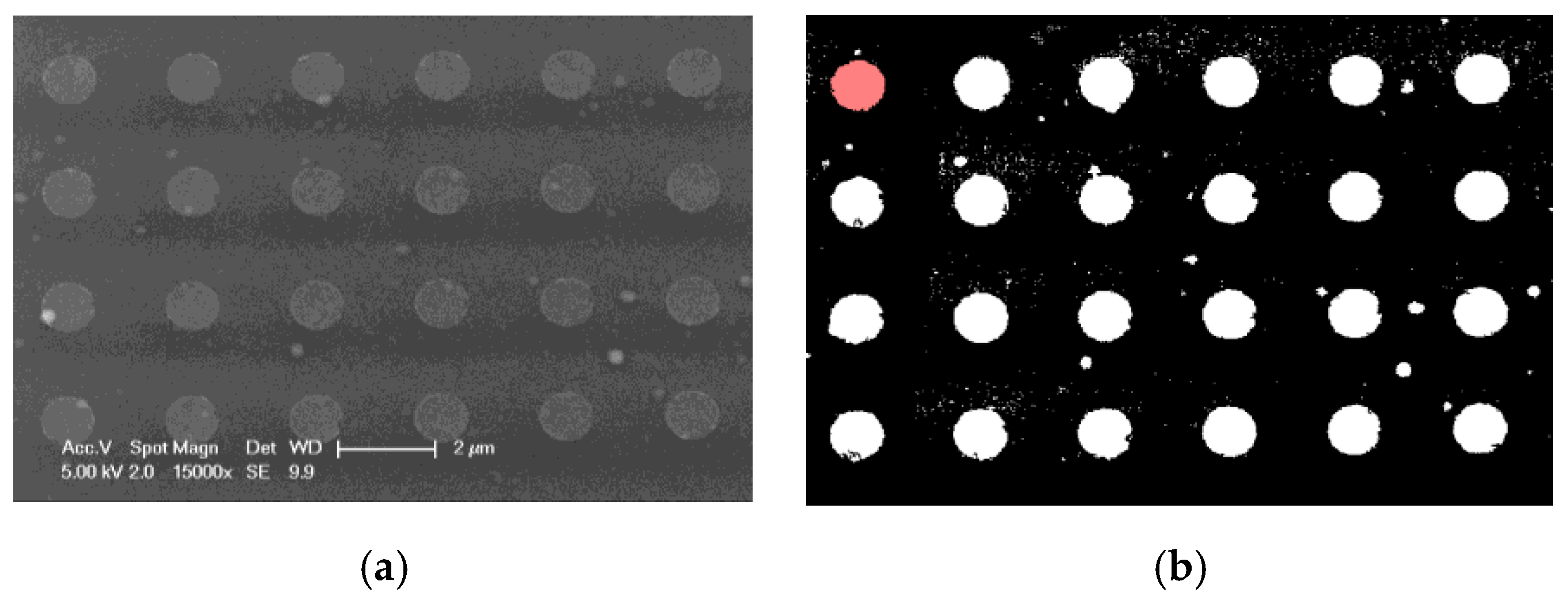
For enabling a quantitative analysis of the effect of size and shape on the performance of the metamaterials, different samples were imaged using SEM. The distribution of size and eccentricity (shape) were analyzed using an image processing algorithm in Matlab.
Figure 5 shows an example of SEM image and its corresponding binary image produced and utilized in the image processing algorithm.
Table 1 lists the statistical results obtained. As expected, larger diameter disks have a lower fabrication defect (lower standard deviation and lower eccentricity).
4. Conclusions
Lithography based fabrication of mid-infrared metamaterial absorbers enables the batch fabrication of the metamaterial absorbers suitable for MEMS applications. As compared to e-beam lithography, the lower level of control on the fabrication parameters as well as the lower minimum feature size available in UV lithography results in a higher level of fabrication errors. Various sources of errors, namely surface roughness, and size distribution, and their corresponding effect on the performance of the metamaterial were identified and analyzed in this work.
The roughness was found to have a significant effect on the Q-factor of the metamaterial absorber. Therefore, optimization of the deposition process of the underlying layers, e.g., backplane metal and spacer, is essential for the fabrication of metamaterials. The effect of lithography based errors on the performance of metamaterial absorbers with different diameter was also analyzed. It was shown that while the tolerance is low for disk diameters larger than 1000 nm, the UV lithography of 900 nm diameter disks resulted in smaller than nominal dimensions. Furthermore, the eccentricity was found to be higher for smaller disks. Such analysis can be used to compensate for shape tolerances in future designs.
Acknowledgments
This work has been supported by the Dutch Technology Foundation STW under Grant DEL.11476. The fabrication process was carried out in the Else Kooi Laboratory (formerly known as Dimes Technology Center), Delft, The Netherlands.
Conflicts of Interest
The authors declare no conflict of interest. The founding sponsors had no role in the design of the study; in the collection, analyses, or interpretation of data; in the writing of the manuscript, and in the decision to publish the results.
References
- Ma, W.; Wen, Y.; Yu, X. Broadband metamaterial absorber at mid-infrared using multiplexed cross resonators. Opt. Express 2013, 21, 30724–30730. [Google Scholar] [CrossRef] [PubMed]
- Karimi Shahmarvandi, E.; Ghaderi, M.; Ayerden, N.P.; de Graaf, G.; Wolffenbuttel, R.F. In CMOS-compatible metamaterial-based wideband mid-infrared absorber for microspectrometer applications. In Proceedings of the SPIE 9883, Metamaterials X, Brussels, Belgium, 3 April 2016. [Google Scholar] [CrossRef]
- Gall, D. Electron mean free path in elemental metals. J. Appl. Phys. 2016, 119, 085101. [Google Scholar] [CrossRef]
- Nagpal, P.; Lindquist, N.C.; Oh, S.-H.; Norris, D.J. Ultrasmooth patterned metals for plasmonics and metamaterials. Science 2009, 325, 594–597. [Google Scholar] [CrossRef] [PubMed]
- Timoshevskii, V.; Ke, Y.; Guo, H.; Gall, D. The influence of surface roughness on electrical conductance of thin Cu films: An ab initio study. J. Appl. Phys. 2008, 103, 113705. [Google Scholar] [CrossRef]
- Drachev, V.P.; Chettiar, U.K.; Kildishev, A.V.; Yuan, H.-K.; Cai, W.; Shalaev, V.M. The ag dielectric function in plasmonic metamaterials. Opt. Express 2008, 16, 1186–1195. [Google Scholar] [CrossRef] [PubMed]
| Publisher’s Note: MDPI stays neutral with regard to jurisdictional claims in published maps and institutional affiliations. |
© 2017 by the authors. Licensee MDPI, Basel, Switzerland. This article is an open access article distributed under the terms and conditions of the Creative Commons Attribution (CC BY) license (https://creativecommons.org/licenses/by/4.0/).


