1. Introduction
Silica Aerogels have porosities of 80–99.8% and pore sizes in the range of 10 nm to 70 nm [
1]. Consequently, these gels are attractive for thermal decoupling due to a very low thermal conductivity of 0.02 W/mK [
1] and have an extremely large inner surface area of up to 1000 m
2/g. Furthermore, silica aerogels are chemically inert as they consist only of silicone oxide (SiO
2) but also transparent with an optical transmission of 90%. By surface modification with hexamethyldisilazane (HMDS), the gels become superhydrophobic [
1]. Therefore, the integration of silica aerogels in microchips is of interest to many MEMS-applications like catalysis reactions, surface modifications (e.g., coating with antibodies), optical measurements or as interface between gases and liquids to solve the gases (e.g., cell cultivation for lab-on-a-chip applications).
Silica aerogels are usually formed in a two step sol-gel process by synthesizing an alcogel from a precursor containing tetraethyl orthosilicate (TEOS) and subsequent aging and drying processes. Due to their porosity, the gels shrink during these processes between 14% and 51% [
1] resulting in cracks or breakage of the gel and preclude the filling of cavities in MEMS. Therefore, silica aerogels have only been integrated into microchips in the form of ground particles as chromatographic stationary phase [
2], but not as a monolith produced inside the chip.
We present an adapted fabrication process that minimizes the shrinkage by adding polyethylene glycol (PEG), extending the aging step and coating the gel with HMDS. This process is used to generate silica aerogels as bulk material in cavities of borosilicate glass.
2. Materials and Methods
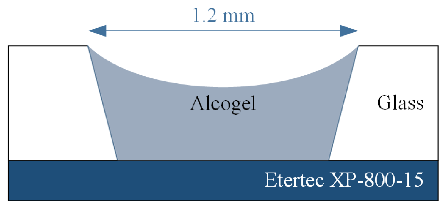
For the experiments a 500 μm thick borosilicate glass wafer which was laminated with i-HE dry-film-resist of Harke GmbH, Germany was used. By using the patterned resist as a mask, holes with a diameter of 1.2 mm were sandblasted. The dry-film-resist Etertec XP-800-15 of Eternal Chemical Co., Ltd., Taiwan was laminated as a removable bottom layer for the sol as shown in
Figure 1. The wafer was diced into chips of 17.5 mm length and 13 mm width.
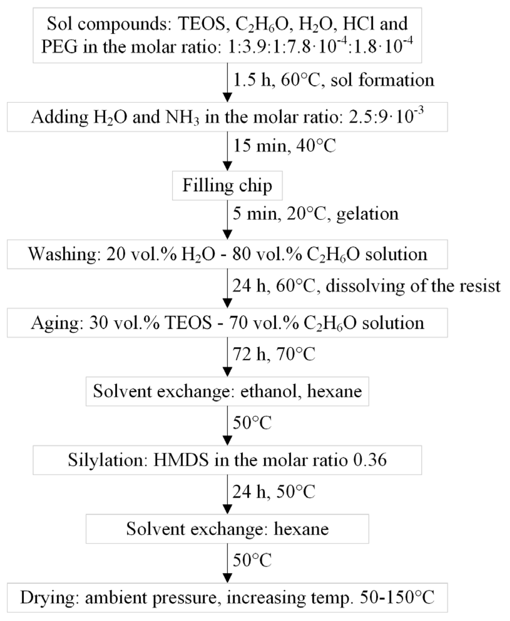
The silica gel is formed by a two-step acid-base sol-gel process. The compounds of the gel, their concentrations and the experimental procedure are presented in
Figure 2. The first step is a hydrolysis reaction of the precursor TEOS with water [
1]:
This reaction is catalysed by the addition of hydrochloric acid. Ethanol serves as solvent. The addition of PEG influences the pore sizes of the gel matrix and the resulting gel gets a higher mechanical strength and shrinks less during the drying process [
3].
In the second step the base catalyst ammonium speeds up polycondensation reactions [
1]:
Clusters are built due to the formation of siloxane bonds. After 15 min of the polycondensation reactions, the holes of the microchip are filled with the solution where the final gelation is carried out. Here polymer chains are formed and the substance turns solid.
During the washing process of 24 h and aging process of 72 h, more cross-linking occurs and the gel matrix is strengthened. Small particles are dissolved and deposited between bigger particles so that the bonds are stabilised [
3]. The dry-film-resist dissolves in the solution due to the ethanol and is removed from the chip in this way. The following silylation with HMDS
results in a hydrophobic aerogel and prevents a reaction of hydroxyl groups during the drying at ambient pressure [
1]. Those would otherwise form additional siloxane bonds when the gel is in a compressed state due to capillary pressure and the gel could not re-expand when the pressure is released.
3. Results and Discussion
Figure 3 shows a photograph of a part of the borosilicate glass chip in which the experiment was carried out. In this device, four out of five holes were filled with the silica aerogel.
To determine the porosity of the silica aerogel, an aerogel block of the same sol composition as used in the filled holes was analysed. The dimensions of the block are 2.9 mm × 2.74 mm × 2.1 mm and its weight is 6.6 mg. Thus the bulk density was calculated as 0.4 g/cm3. The skeletal density was presumed as 2.65 g/cm3 which is the density of SiO2 resulting in a porosity of 85%.
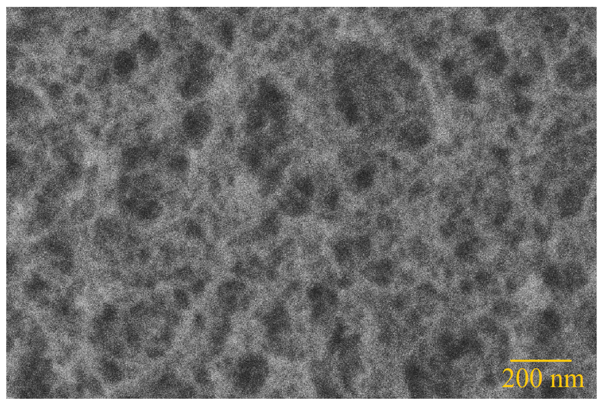
The structure of the silica aerogels was further analysed in a SEM as presented in
Figure 4. As expected the structure is a highly porous network. The measurements show pore diameters between 20 nm and 80 nm with an average pore size of 50 nm.
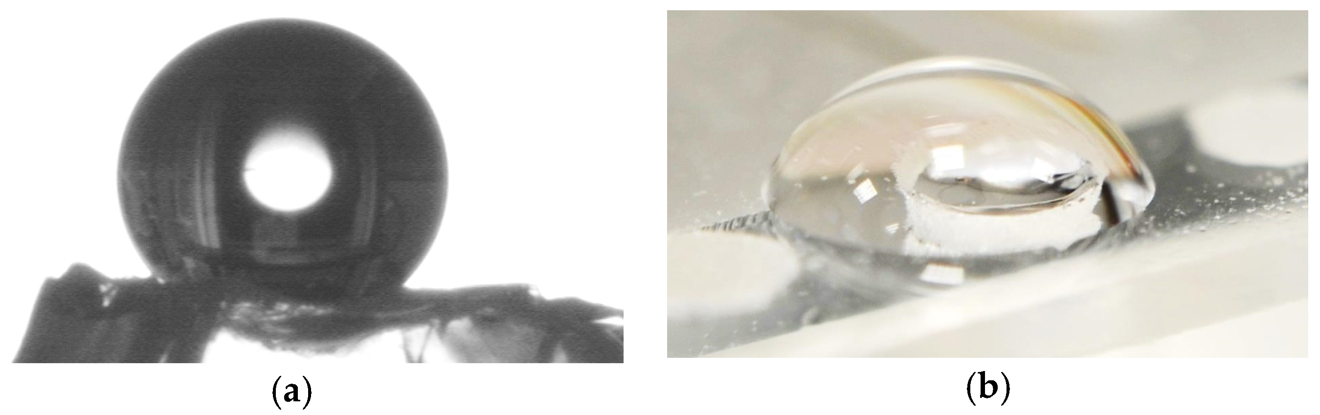
Due to the coating with HMDS, the gel became hydrophobic. The contact angle was determined as 136° on a silica aerogel block shown in
Figure 5a. Water is not sucked into the highly porous aerogel. Therefore, a droplet of water does not flow through the hole containing the gel as pictured in
Figure 5b in contrast to a hole without aerogel.
4. Conclusions
For the first time a method to integrate silica aerogels as bulk material monolithically into microchips is presented. The two step sol-gel process is used to synthesize the gel from the precursor TEOS. The addition of PEG, the extended aging process and the surface modification with HMDS increase the strength of the gel and result in hydrophobic aerogels with high porosity of 85%. Furthermore, the shrinkage during the solvent exchanges, silylation and drying is minimized which allows the filling of holes in a borosilicate glass with a diameter of 1.2 mm with silica aerogel. Without the presented modifications, the aerogel either cracks or crumbles during drying process or does not adhere and falls off the chip.
Due to its high porosity and the hydrophobicity, the gel contains much air but cannot be penetrated with liquids. Therefore this technology is of interest for microfluidic applications that require a stable liquid-gas interface without leakage of the fluid. Furthermore, the high porosity and the small pores between 20 nm and 80 nm result in very high inner surfaces that are attractive for surface modifications but also thermal isolation.
Acknowledgments
This work is a part of the research project “LifeChip” which is supported by the Federal Government’s and Federal States’ Excellence Initiative in the framework of the institutional strategy of University of Bremen, Germany.
Conflicts of Interest
The authors declare no conflict of interest. The founding sponsors had no role in the design of the study; in the collection, analyses, or interpretation of data; in the writing of the manuscript, and in the decision to publish the results.
References
- Rao, A.P.; Pajonk, G.M.; Rao, A.V. Effect of preparation conditions on the physical and hydrophobic properties of two step processed ambient pressure dried silica aerogels. J. Mater. Sci. 2005, 40, 3481–3489. [Google Scholar] [CrossRef]
- Gaspar, A.; Nagy, A.; Lazar, I. Integration of ground aerogel particles as chromatographic stationary phase into microchip. J. Chromatogr. A 2011, 1218, 1011–1015. [Google Scholar] [CrossRef] [PubMed][Green Version]
- Soleimani Dorcheh, A.; Abbasi, M.H. Silica aerogel; synthesis, properties and characterization. J. Mater. Process. Technol. 2008, 199, 10–26. [Google Scholar] [CrossRef]
| Publisher’s Note: MDPI stays neutral with regard to jurisdictional claims in published maps and institutional affiliations. |
© 2017 by the authors. Licensee MDPI, Basel, Switzerland. This article is an open access article distributed under the terms and conditions of the Creative Commons Attribution (CC BY) license (https://creativecommons.org/licenses/by/4.0/).


