1. Introduction
The field of microfluidics is rapidly expanding, and as a result the need for advanced microchannel fabrication technologies. The majority of the silicon based microfluidic devices, especially those with wide and/or deep microchannels like for instance integrated circuits for cooling or gas chromatography, are still sealed with wafer bonding techniques [
1,
2]. This cumbersome method limits miniaturization and further system integration possibilities.
Previous studies have already shown that it is possible to fabricate CMOS compatible microchannels that allow for the addition of actuators/sensors [
3,
4]. Furthermore, a recently proposed method for a two-step fabrication of sealable microchannels through a mesh mask, facilitates the development of the silicon based platforms like for instance Lab-on-a-Chip (LOC) or Organ-on-a-Chip (OOC). These high resolution silicon based microfluidic devices enable miniaturization and allow for further wafer processing and thus integration of actuators or sensors for in-situ stimulation or measurement. However, the major drawback of this method is the limited depth of the microfluidic channels, with maximum aspect ratio of 4, due to the saturation in the DRIE (Deep Reactive Ion Ethcing) of narrow trenches at a depth of about 40 µm [
5].
This paper introduces a new CMOS compatible method for the fabrication of fully embedded multidimensional microchannels with high aspect ratio (HAR) in a single DRIE step.
2. Materials and Methods
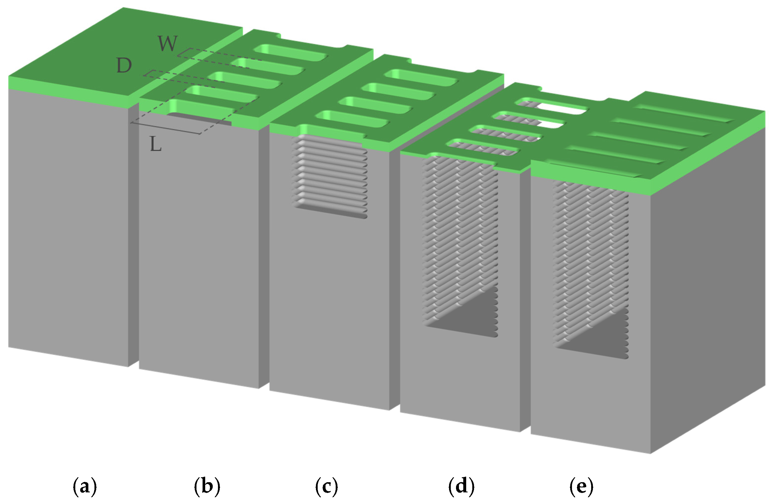
The fabrication starts with the depositions of a 2 μm thick layer of low-stress PECVD SiO
2 on a silicon substrate. At the location of test channels, rows of parallel arrays with 56 different combinations of sub-micron size rectangular slits are dry-etched in the silicon dioxide using standard photoresist mask. The slits dimentions (see
Figure 1) are varried as follows:
Slit lenght (L): 6.0 μm; fixed,
Slit width (W): 0.8 μm, 1.0 μm, 1.2 μm, 1.4 μm, 1.6 μm, 1.8 μm, 2.0 μm; variable,
Slit distance (D): 0.6 μm, 0.8 μm, 1.0 μm, 1.2 μm, 1.4 μm, 1.6 μm, 1.8 μm, 2.0 μm; variable.
Subsequently, channels in the silicon are etched through the meshed SiO
2 hard mask in a single DRIE using the Bosch process. In this process cycles of: dry silicon etch (using SF
6), walls passivation (using C
4F
8), and break-through the passivation layer on the bottom of the trench; are alternatively performed and repeated in number of loops. This results in deep trenches with straight walls in the silicon.
Figure 1 shows the graphical representation of the fabrication stages.
The duration of the silicon etch cycle varries from 1.5 s through 4 s up to 8 s. The number of etch-passivation loops, and thus the total etch time, is increased from 10 loops up to 150 loops for long etch cycles (8 s) and up to 500 loops for short etch cycles (1.5 s). The total etch time is limited in such a way that at least 500 nm of the silicon dioxide hard mask is preserved on top of each channel. The preserved mesh mask is closed with a 2.5 μm thick layer of PECVD SiO2 to form the embedded network of microchannels.
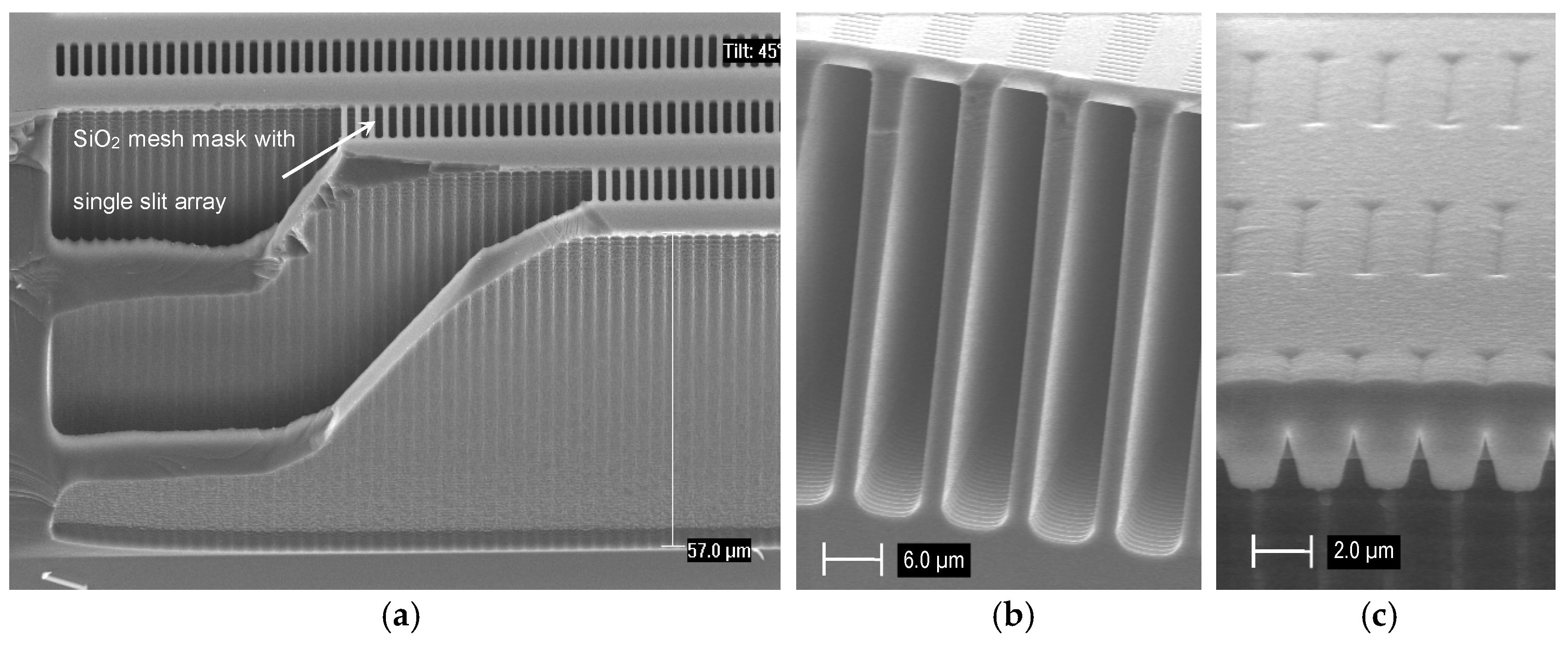
The cross-section of each fabcricated channel is inspected in 45° and 90° tilt with SEM (Scanning Electron Microscope) to determin its depth and shape, and to examine the silicon dioxide mesh mask before and after closing the channel.
3. Results and Discussion
A number of microchannels were etched in silicon through the 2 µm thick hard etch mask of silicon dioxide. At first it was observed that very uniform (approximately 590 µm long and 6 µm wide) channels with a depth of almost 60 µm were etched in the silicon when the walls between single trenches were removed (
Figure 2a). This results in aspect ratios of up to 10. The maximal reached depth of the trench was limited only by the thickness of the SiO
2 mask, which had to be preserved in order to allow for CMOS-compatible and low-topography sealing of the structures with PECVD SiO
2 (
Figure 2b,c).
The mechanism of etching trough the fine mesh mask and related to it walls removal was further studied in respect to process parameters: the etch cycle time and the number of etch-passivation loops; and design parameters: the slits width and the distance between the slits (slits length is fixed).
3.1. Process Parameters
To test the influence of process parameters on the channels formation and their etch rate, three series of wafers with etch cycle times
tecth = {1.5 s; 4.0 s; 8.0 s}, and increasing number of etch-passivation loops were etched through the oxide mesh with the same, fixed slits dimensions. The dependence on the trench depth from the total etch time,
ttotal was calculated from:
where
toveretch is the time of the silicon etch during the passivation break-through cycle after the passivation layer has been removed (
toveretch = 1 s), was ploted in
Figure 3a. For short total etch time (
ttotal ≤ 250 s) the etch rates and reached depths are comparable for all three series. For longer total etch time (
ttotal > 250 s), the walls between trenches with smaller scallops (
tetch = 1.5 s) are still present, and a slight trench depth saturation can be observed. For trenches with bigger scallops (
tetch = {4 s; 8 s}) the walls were removed at
ttotal ≈ 800 s and
ttotal ≈ 400 s respectively (the exact wall removal moment is hard to determine as it is a gradual process). The walls removal is directly connected with the shift in the etch rate curve allowing for achieving HAR structures without noticeable saturation signs within this experiment.
3.2. Design Parameters
In the second experiment the process parameters were fixed (90 loops,
tetch = 8 s) while the mesh mask design parameters were varied: W [µm] = {0.8; 1.0; 1.2; 1.4; 1.6; 1.8; 2.0}, D [µm] = {0.6; 0.8; 1.0; 1.2; 1.4; 1.6; 1.8; 2.0}; resulting in channels with various depths. The dependence of the trench depth on the slit parameters: width
W and the distance between the slits
D is plotted in
Figure 3b. The trench depth is directly proportional to W, corresponding to the open mask area, and inversely proportional to D, corresponding to the trench wall thickness. The increase of the channels depth with decreasing slits distance is only noticable after the walls removal and thus formation of the channel. The thinner the walls between trenches is, the faster they merge into channels preventing its DRIE etch saturation.
4. Conclusions
With the new single-step DRIE process presented in this paper, it is possible to etch multidimetional microchannels with a uniform detpth and high aspect ratio of up to 10. By modifying the hard etch mesh mask design parameters (slit dimensions) and the Bosch process (DRIE) parameters, it is possible to simultaneously etch trenches and remove the walls between them forming a channel underneath the hard etch mesh mask. The channel formation underneath the mask changes the etching mechanism preventing DRIE etch saturation and therefore allows for the fabrication of HAR microchannels. After etching, the remaining mesh mask can be closed with PECVD SiO2 to form the embedded microchannels. Channels with different dimensions can be etched in the same single-step process by tuning the mask design parameters.
Future work will include application studies, such as the integration of sensors on top of the embedded microchannels, and optimization of the mask in order to be able to reach even higher aspect ratios.
Acknowledgments
This research and resulting paper were carried on within InForMed project funded by ECSEL JU grant no: 2014-2-662155. The experiments and measurements were conducted in the Else Kooi Laboratory—CL100 cleanroom facility.
Conflicts of Interest
The authors declare no conflict of interest. The founding sponsors had no role in the design of the study; in the collection, analysis, or interpretation of data; in the writing of the manuscript, and in the decision to publish the results.
References
- Zhang, X.; Han, X.; Sarvey, T.E.; Green, C.E.; Kottke, P.A.; Fedorov, A.G.; Joshi, Y.; Bakir, M.S. Three-Dimensional Integrated Circuit With Embedded Microfluidic Cooling: Technology, Thermal Performance, and Electrical Implications. J. Electron. Packag. 2016, 138, 1–9. [Google Scholar] [CrossRef]
- Lambertus, G.; Elstro, A.; Sensenig, K.; Potkay, J.; Agah, M.; Scheuering, S.; Wise, K.; Dorman, F.; Sacks, R. Design, fabrication, and evaluation of microfabricated columns for gas chromatography. Anal. Chem. 2004, 76, 2629–2637. [Google Scholar] [CrossRef]
- Huang, Y.; Mason, A.J. Lab-on-CMOS Integration of Microfluidics and Electrochemical Sensors. Lab. Chip 2013, 13, 3929–3934. [Google Scholar] [CrossRef]
- Dijkstra, M.; De Boer, M.J.; Berenschot, J.W.; Lammerink, T.S.J.; Wiegerink, R.J.; Elwenspoek, M. A versatile surface channel concept for microfluidic applications. J. Micromech. Microeng. 2007, 17, 1971. [Google Scholar] [CrossRef]
- Stoute, R.; Muganda, J.M.; Dahar, S.; Arslan, A.; Henderikx, R.J.M.; van Stiphout, P.C.M.; den Toonder, J.M.J.; Dekker, R. CMOS Compatible Embedded Microchannels. In Proceedings of the 20th International Conference on Miniaturized Systems for Chemistry and Life Sciences, Dublin, Ireland, 9–13 October 2016. [Google Scholar]
| Publisher’s Note: MDPI stays neutral with regard to jurisdictional claims in published maps and institutional affiliations. |
© 2017 by the authors. Licensee MDPI, Basel, Switzerland. This article is an open access article distributed under the terms and conditions of the Creative Commons Attribution (CC BY) license (https://creativecommons.org/licenses/by/4.0/).


