Article

Screen-Printed Metamaterial Absorber Using Fractal Metal Mesh for Optical Transparency and Flexibility

Department of Intelligent Semiconductor Engineering, Chung-Ang University, Seoul 06974, Republic of Korea
*
Author to whom correspondence should be addressed.
Fractal Fract. 2024, 8(5), 284; https://doi.org/10.3390/fractalfract8050284
Submission received: 3 April 2024 / Revised: 4 May 2024 / Accepted: 6 May 2024 / Published: 9 May 2024
(This article belongs to the Special Issue Advances in Fractal Antennas: Design, Modeling and Applications)

Abstract

:
In stealth applications, there is a growing emphasis on the development of radar-absorbing structures that are efficient, flexible, and optically transparent. This study proposes a screen-printed metamaterial absorber (MMA) on polyethylene terephthalate (PET) substrates using indium tin oxide (ITO) as the grounding layer, which achieves both optical transparency and flexibility. These materials and methods enhance the overall flexibility and transparency of MMA. To address the limited transparency caused by the silver nanoparticle ink for the top pattern, a metal mesh was incorporated to reduce the area ratio of the printed patterns, thereby enhancing transparency. By incrementing the fractal order of the structure, we optimized the operating frequency to target the X-band, which is most commonly used in radar detection. The proposed MMA demonstrates remarkable performance, with a measured absorption of 91.99% at 8.85 GHz and an average optical transmittance of 46.70% across the visible light spectrum (450 to 700 nm), indicating its potential for applications in transparent windows or drone stealth.

1. Introduction

Advancements in detection technology have taken various forms [1]. Sonar systems measure reflected sound waves, whereas radar systems measure reflected electromagnetic waves. Both systems activate after these waves strike a target, facilitating the detection and measurement of the target’s distance [2,3]. Infrared detectors are commonly employed to sense and visualize the thermal radiation patterns emitted by all objects [4]. Visible light detection functions by capturing light reflected from a target and is observable by the naked eye or a camera. Given the simultaneous use of various detection technologies, stealth must be concurrently incorporated across all methods. For instance, in a detection system that uses both radar and cameras for surveillance, the counter-detection system must effectively evade both radar and visible detection. Focusing solely on stealth in one domain is inadequate for avoiding detection.
Radar detection, which typically operates within the X-band to achieve optimal resolution and range, relies on the radar cross-section (RCS) to identify targets [5]. This is critical because an aircraft with a low RCS, smaller than that of a bird, for instance, can significantly reduce a radar’s ability to track it [6]. Achieving electronic wave absorption is critical for evading radar detection by minimizing reflection and reducing RCS. There are two common methods for achieving radar absorption, radar-absorbing materials (RAM) and radar-absorbing structures (RAS). RAMs provide benefits such as wide bandwidth and insensitivity to incident angles, often incorporating high magnetic materials or composites [7]. In addition, cost-effective and easily maintainable RASs, such as Salisbury screens and Dallenbach layers, are commonly used [8,9,10]. RAM and RAS complement each other’s advantages and can be synergistically employed [11].
The use of metamaterials as absorbers has recently garnered significant attention because of their thin profile, controllable and scalable working frequencies, and perfect absorption performance [12]. Metamaterials, characterized by their artificial composition consisting of periodic arrays of unit structures, are designed to exhibit properties uncommon to natural materials, such as negative refractive indices. This distinctive feature presents diverse opportunities for electronic applications [13,14]. Metamaterial unit structures are scaled smaller than the wavelength of interest, allowing each unit to act as an individual particle [15]. In these designed unit structures, the properties of the materials are not analyzed based on their individual permittivity or permeability but are considered in terms of effective permittivity and permeability. By leveraging these adjustable electronic properties, the reflection coefficient is minimized through impedance matching between the metamaterials and free space, thereby optimizing their function as absorbers [16].
To evade detection by visible light, metamaterial absorbers (MMA) can employ two primary approaches, camouflage or transparency. Camouflage adapts to visual detection by mirroring the colors of the surrounding environment. Transparency can be achieved in the following two ways, similar to radar absorption techniques: material selection and structural design. Constructing devices with transparent substances such as polyethylene terephthalate (PET) and polymethyl methacrylate (PMMA) is one such strategy [17,18,19]. Moreover, transparent conductive materials such as indium tin oxide (ITO) and silver nanowires are viable options [20,21]. Structurally, transparency is achieved by reducing the area ratio of non-transparent materials in the MMA composition. Metal mesh or metal wire patterns are commonly incorporated to achieve transparency [22,23]. This approach offers the dual benefit of providing electromagnetic shielding while allowing light transmission. Within MMAs, a metal mesh is typically integrated into the ground layer to enhance flexibility and transparency. The empty spaces in the mesh allow visible light to pass through, while the metal’s high conductivity provides electromagnetic shielding.
PET substrates are used not only for their transparency but also for their flexibility [24,25,26]. ITO or silver nanoparticle inks are employed as flexible conductors, contributing to the overall flexibility of the fabricated MMAs [27,28]. The fabrication method for these materials is particularly well-suited to screen-printing technology, which leverages masks to facilitate high-resolution printing on various flexible substrates [29,30]. Screen printing offers a simple, cost-effective, and rapid process, providing significant advantages in mass production capabilities compared to inkjet printing or laser alignment [31,32].
This article introduces the innovative use of fractals in conjunction with metal mesh in MMAs. Departing from the conventional use of metal mesh as a ground plate [33,34], this approach positions the metal mesh at the top layer to simultaneously enhance flexibility and transparency. Fractals are commonly used in electronic devices to enable multi-band operation or miniaturization [35,36,37,38,39]. In this study, fractals were used to optimize the resonant frequency within the targeted X-band. The developed MMA achieved a remarkable absorptivity of 91.99% at 8.85 GHz, aligning with the standard requirements for MMAs. In addition, the material achieved a transparency of 46.70% across the wavelength spectrum from 450 to 700 nm.

2. Design and Analysis

2.1. Geometric Structure and Simulation Setup

Figure 1a illustrates the proposed MMA, which comprises two conductive layers separated by a dielectric substrate. The top layer utilizes silver nanoparticle ink (INK), specifically DM-SIP-3072S (Dycotec Materials, Calne, UK), with a sheet resistance of 0.4 Ω/sq. The dielectric layer is composed of a transparent, flexible PET with a relative dielectric constant of 3.16 and a loss tangent of 0.0073. A continuous ITO film forms the bottom layer, exhibiting a resistance of 7 Ω/sq. The thicknesses of the PET substrate are 1.50 mm (t).
Figure 1b illustrates a top view of the MMA, depicting a unit structure that maintains its configuration after a 90° rotation. This unit cell is characterized by a second-order fractal design comprising square rings of uniform wire width that progressively increase with each iteration. The largest square ring, positioned at the center, has an inner side length of 2.4 mm, followed by the medium-sized square ring at 1.6 mm, and the smallest square ring at 0.8 mm. These rings are interconnected by the shared conductive wire sides. In our simulations, we defined the structural parameters as follows: periodicity (p) of 8.9 mm and wire width (w) of 0.2 mm.
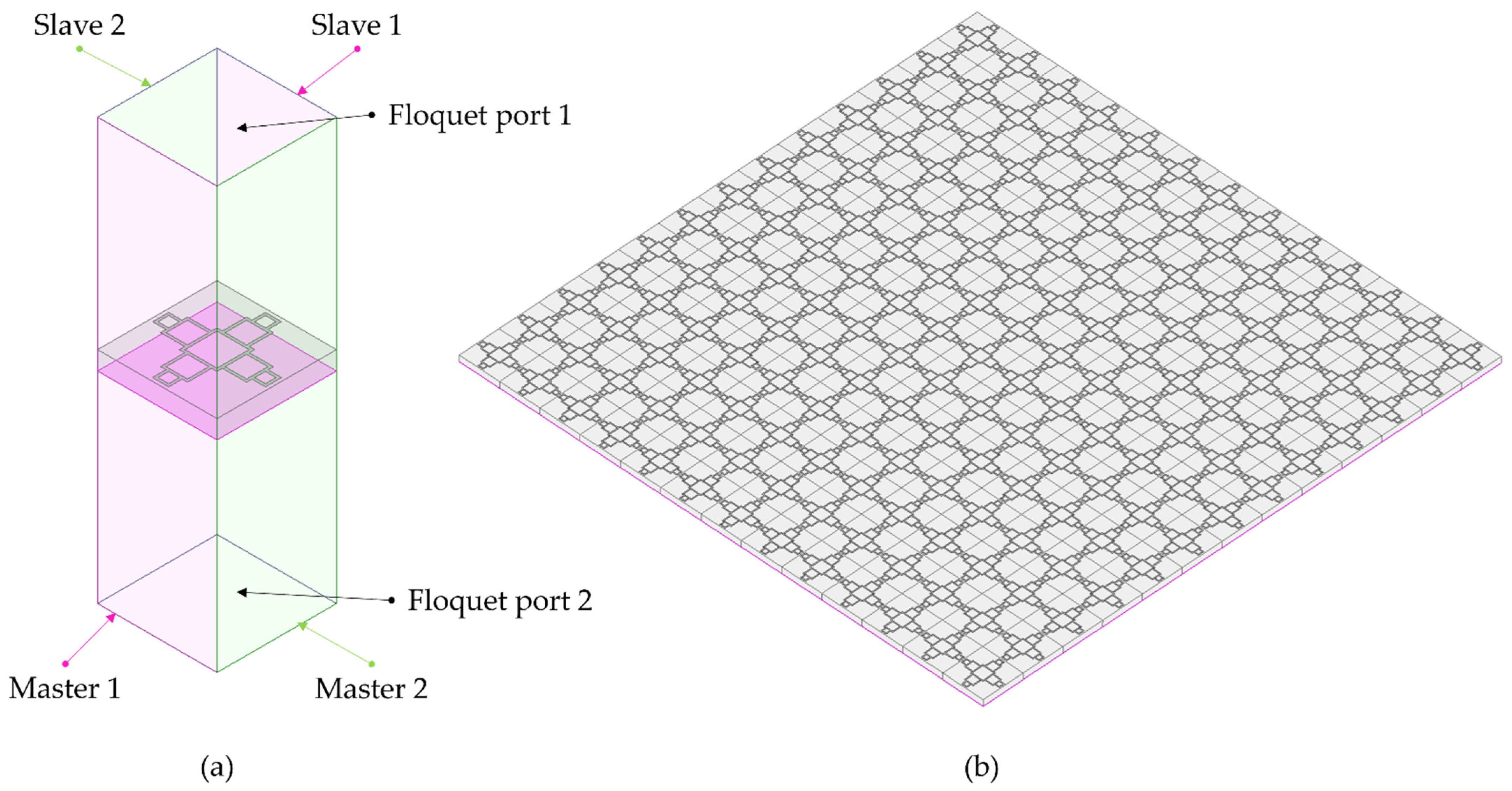
Simulations were conducted using a high-frequency structure simulator (HFSS, ANSYS, Canonsburg, PA, USA). As illustrated in Figure 2a, the parallel side faces of the unit cell were configured as master and slave to simulate an infinite array. Floquet ports were assigned to the top and bottom faces to facilitate the boundary conditions for the electromagnetic analysis. The result is a metal mesh form, as shown in Figure 2b, due to the periodic array.
The absorptivity ( A ω ) of the MMA is derived from the magnitude of the reflection coefficient ( R ω ) and transmission coefficient ( T ω ), according to the following equation:
A ω = 1 R ω T ω = 1 S 11 2 S 21 2
where ω denotes the angular frequency of the incident electromagnetic wave. In this context, R ω = S 11 2 represents the square of the reflection coefficient, signifying the proportion of the reflected wave, and T ω = S 21 2 indicates the square of the transmission coefficient, representing the proportion of the transmitted wave. It is customary to consider 90% absorptivity as the benchmark for bandwidth; this standard was adopted in the current study.

2.2. Principle of Metamaterial Absorber

To achieve optimal absorptivity, it is essential to reduce both the transmission and reflection coefficients. The high conductivity of the ground plane results in impedance approaching zero, which in turn, leads to near-total reflection and negligible transmission. Conversely, impedance matching between the metamaterial and free space minimizes the reflection coefficient.
S 11 = Z M ω Z 0 Z M ω + Z 0
Equation (2) expresses the reflection coefficient under normal incidence, where Z M ω denotes the impedance of the metamaterial. Z 0 represents the impedance of free space.
Z M ω = μ 0 μ r ω ε 0 ε r ω = Z 0 μ r ω ε r ω
Given that metamaterials comprise composite materials rather than single media, the permittivity and permeability are construed as effective permittivity and effective permeability, represented by μ r ω   and ε r ω , respectively. This relationship is defined in Equation (3). Manipulating its structure allows for the customization of the electromagnetic characteristics of the metamaterial [12].
Figure 3a depicts the proposed metamaterial absorber modeled as a lumped element RLC circuit and a transmission line [40]. Within the equivalent circuit, the thin current-carrying wire is modeled as an inductance, while the coupling between unit structures or between layers is represented by capacitance.
Z i n = Z F S S | | Z T L
The input impedance, Z i n , is the parallel of the impedance of the RLC and the transmission line.
  Z F S S = R + j ω L + 1 j ω C
The top pattern of the MMA is functionally equivalent to a series RLC component, with Z F S S representing its impedance.
β = ω c 0 ε r μ r
  Z T L = Z d Z L + j Z d t a n β d Z d + j Z L t a n β d
Meanwhile, Z T L signifies the transmission line’s impedance, which is determined by aspects such as characteristic impedance, load impedance, permittivity, permeability, frequency, and the transmission line’s length. By integrating Equations (4)–(7) the input impedance Z i n can be represented using the parameters of the equivalent circuit. As described in Equation (2), in the equivalent circuit model, the reflection coefficient is minimized when the input impedance is matched with the impedance of free space. Consequently, as stated in Equation (1), the absorptivity is increased.
Utilizing the Advanced Design System (ADS, Keysight, Santa Rosa, CA, USA) simulation tool, concordance between the HFSS simulation and the equivalent circuit model was confirmed. Software (ADS 2016.01) optimization yielded R = 18.92 Ω, L = 2.15 nH, C = 84.83 fF, and ZL = 7.00 Ω. Figure 3b illustrates that employing these optimized parameters ensures agreement between the outcomes of both simulations.

2.3. Simulation Result

Figure 4 illustrates the distribution of electromagnetic fields at a resonant frequency of 8.98 GHz, highlighting the phases with the highest values. Figure 4a shows the electric field distribution of the proposed MMA, with peak intensities at the square termini. Figure 4b depicts the current density across the top pattern, with current predominantly traversing the top and bottom regions of the central five squares. Figure 4c illustrates the current density within the bottom ground layer, highlighting that the current primarily circulates through the central portion of the bottom layer, flowing in a direction opposite to that of the top layer. The structural unit comprising the top layer is instrumental in facilitating electrical resonance, whereas the overall structure promotes magnetic resonance, thus enabling efficient coupling of electromagnetic radiation to the resonant structure and effective impedance matching [41].
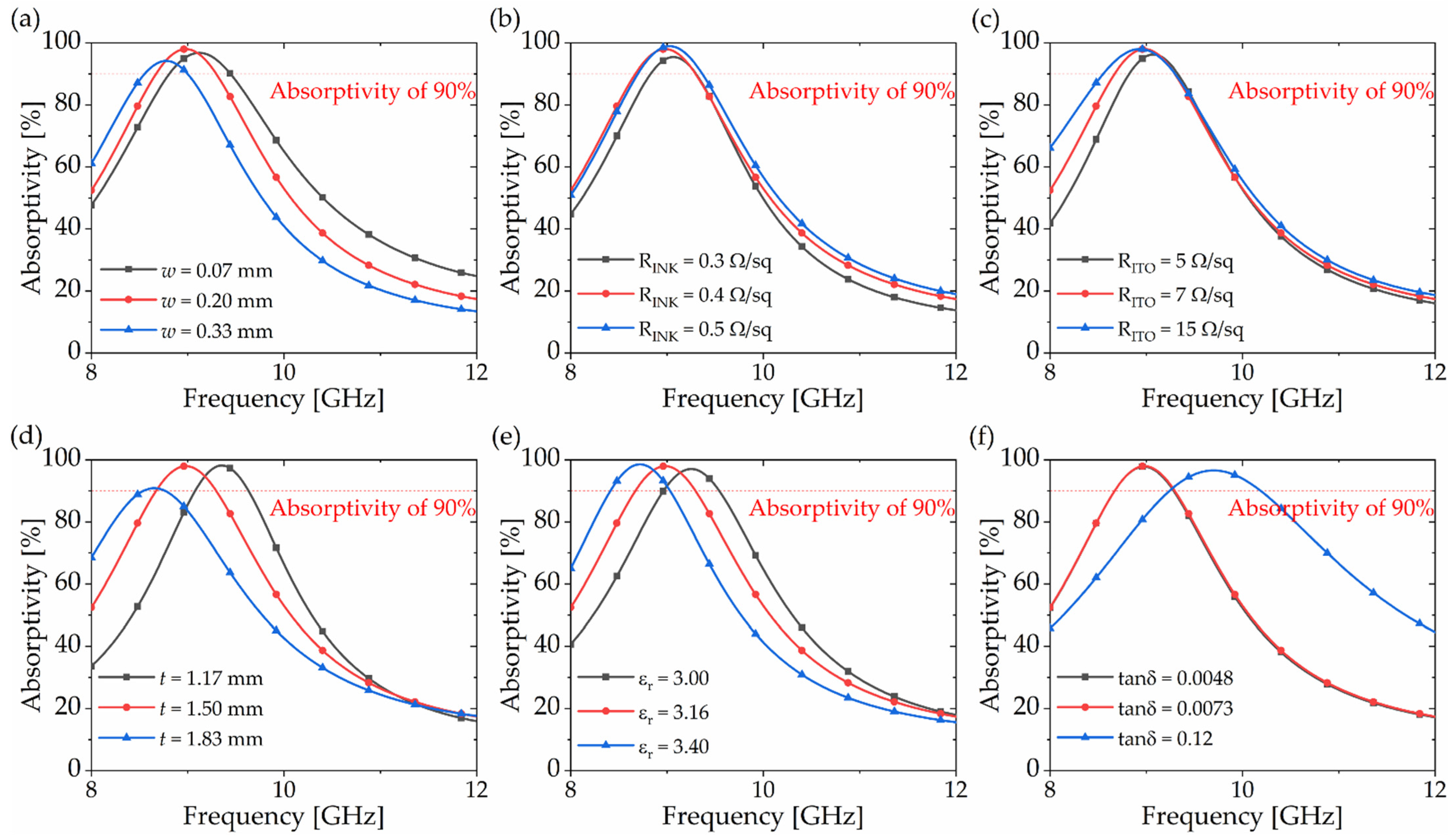
Figure 5 shows a parametric study on factors influencing the absorption rate and frequency; Figure 5a–c detail the primary factors affecting equivalent inductance, and Figure 5d–f explore the impact of substrate characteristics on equivalent capacitance. This study aids in optimizing design and addressing unforeseen effects.
Figure 5a shows that absorptivity is optimized at a specific wire width, with increases in wire width leading to decreases in absorption frequency. Figure 5b,c illustrate that an increase in the sheet resistance of silver ink and ITO films slightly enhances both absorptivity and absorption frequency. Figure 5d confirms that absorptivity is optimized at a particular substrate thickness, with thicker substrates resulting in lower absorption frequencies. In Figure 5e, an increase in the substrate’s permittivity is shown to decrease the absorption frequency. Lastly, Figure 5f indicates that a higher loss in the substrate leads to a wider bandwidth.
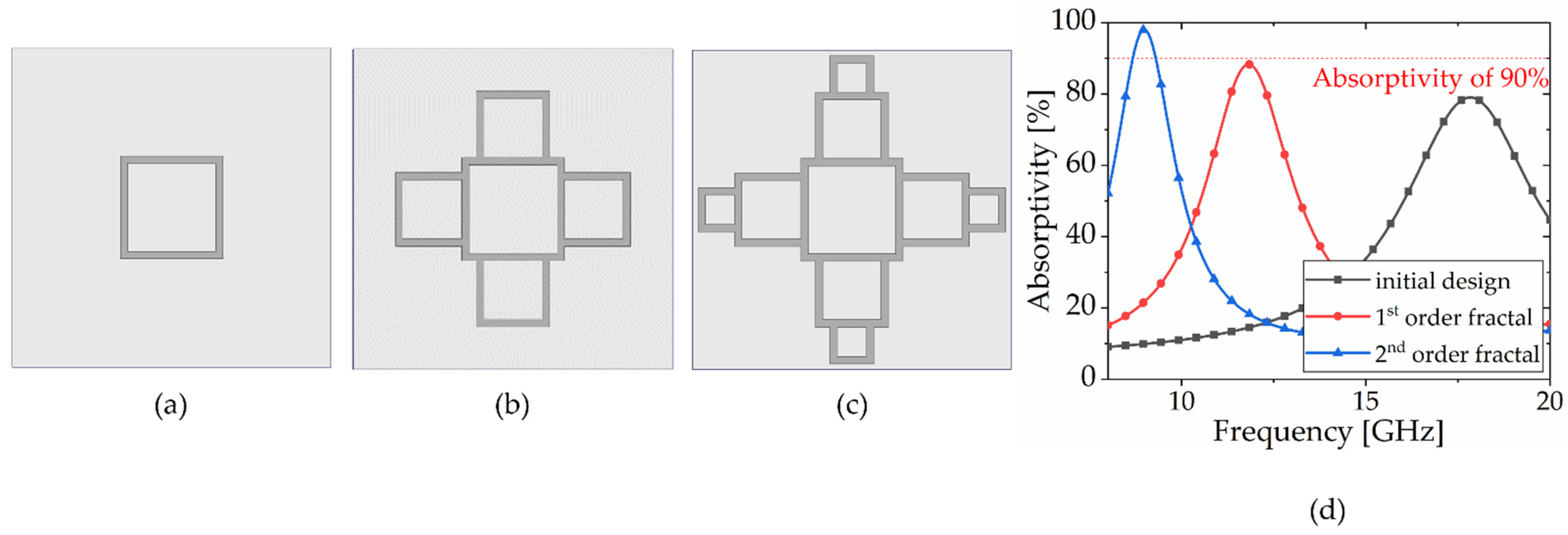
Figure 6 illustrates the absorptivity curves for successive order iterations of a fractal. The curves represent a single square (initial design), a fractal comprising five squares (first-order iteration), and a fractal comprising nine squares (second-order iteration). The plot reveals that higher-order fractals exhibit resonance at lower frequencies. Notably, the absorptivity peaks vary across designs; the initial design reaches its peak at 79.03% at 17.84 GHz, the first iterative design achieves 88.31% at 11.82 GHz, and the second iterative design peaks at 98.07% at 8.98 GHz. By leveraging the space-filling capabilities of the fractal iterations, we achieved frequency optimization. This approach ensures that the final design is finely tuned to precisely match the target frequency.
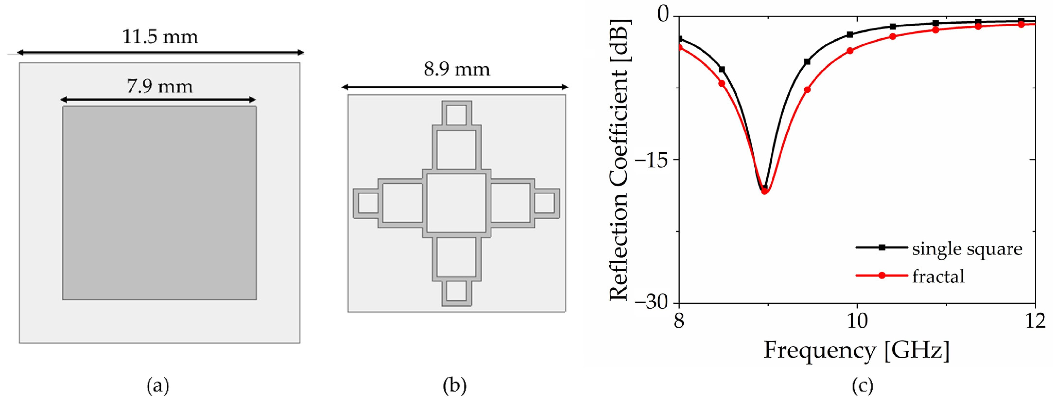
As shown in Figure 7, the single-square design can also achieve similar absorptivity to the proposed fractal design. However, the fractal design exhibits two distinct advantages, including enhanced transparency to visible light and a more compact unit structure compared to the single-square design. When transparency is defined as the ratio of the area devoid of conductor patterns to the total unit area [42], the transparency of the fractal design is 89.29%, while that of the single-square design is 47.19%. Therefore, the fractal design achieves higher transparency compared to the single-square design. In addition, the unit cell size of the fractal design is 8.9 × 8.9 m2, while that of the single-square design is 11.5 × 11.5 mm2 to achieve the same resonant frequency as shown in Figure 7. Therefore, the fractal design can reduce the unit cell size compared to the single-square design.
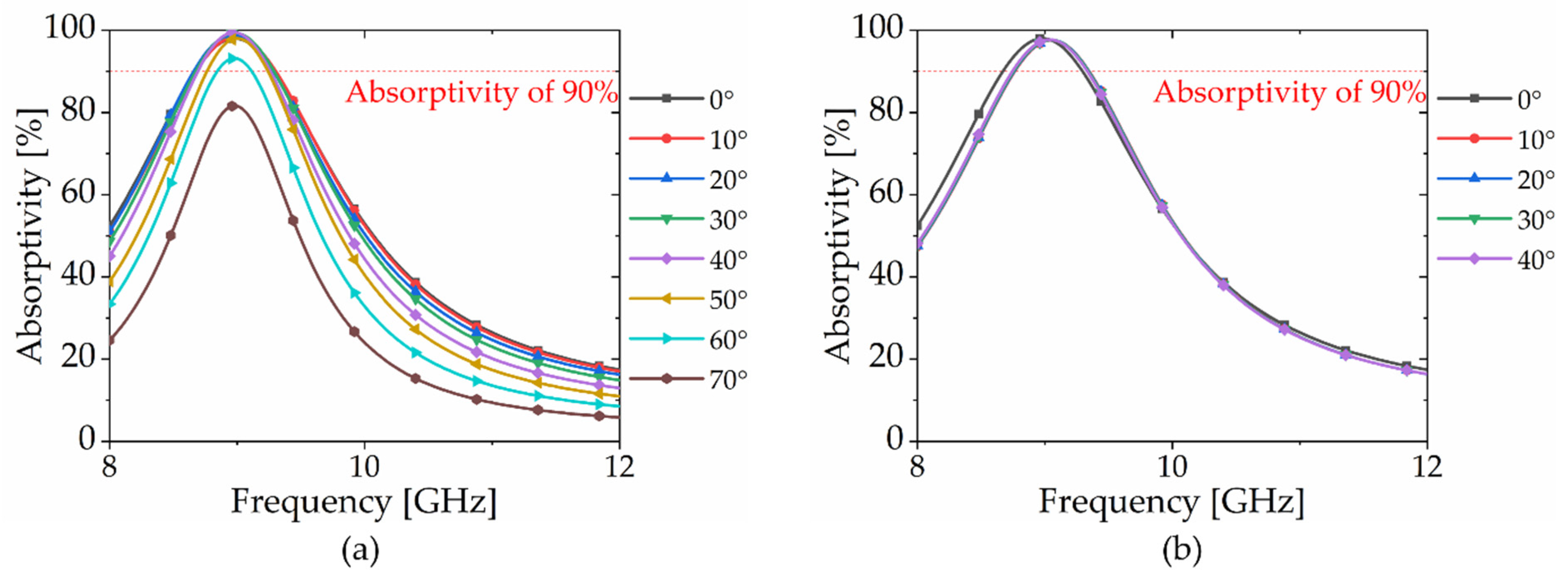
Figure 8a investigates the absorptivity of incident waves at varying angles. The results indicate that the absorptivity exceeds 90% at an incidence angle of 60°, reaching a maximum of 93.18%. Conversely, the absorptivity falls below 90% at an incidence angle of 70°, achieving only 81.64%. Figure 8b investigates the absorptivity of the incident waves under various polarization conditions. Although the proposed MMA exhibits symmetry at intervals of 90°, it was evaluated for polarization up to 45°. The results demonstrate polarization insensitivity, with absorptivity exceeding the 90% threshold across all tested angles, thereby affirming the effectiveness of MMA across a broad range of incident angles and polarization states.

3. Fabrication and Measurement

3.1. Fabrication

Figure 9 illustrates the screen-printing process in detail. The screen frame engraved with the desired pattern is shown in Figure 9c. In the screen frame, the blue areas are where ink cannot pass through, and the white areas allow ink to pass through. Figure 9a illustrates a side view of the situation before printing. Figure 9d illustrates the screen-printing machine for the squeegee operation. The successful transfer of the pattern onto the film is shown in Figure 9b. The sintering process facilitates solvent evaporation, thereby finalizing the film.
The samples of the proposed metamaterial absorber (MMA) were fabricated by layering multiple sheets of 0.25 mm thick PET films (UC224, Hyosung Chemical, Seoul, Republic of Korea) and 0.07 mm thick adhesive films (ARcare® 92561, Adhesives Research, Glen Rock, PA, USA). The electrical properties of the materials are characterized by the resonant cavity method. For instance, the complex permittivity of the PET film bonded by the adhesive film is measured using the split cylinder resonator (N1501AKEAD-710, Keysight, USA) at room temperature. Its relative permittivity and loss tangent are 3.16 and 0.0073, respectively.
Additional PET films and adhesive films are laminated to control the thickness of the screen-printed PET film and MMA, as illustrated in Figure 10. During the lamination process, air may enter, causing variations in the distance between the pattern and the ground and, consequently, affecting the dielectric properties of the substrate. To mitigate this, a presser is utilized to prevent the formation of air layers. Pressure, sufficient to prevent pattern deformation, is applied from one end to the other using a presser longer than one side of the PET film, aiming to remove air as effectively as possible. Subsequently, a 0.18 mm ITO-coated PET film (ITO film, Guluo Glass, Luoyang, China) was affixed to the ground plane of the bottom layer using the same lamination method.
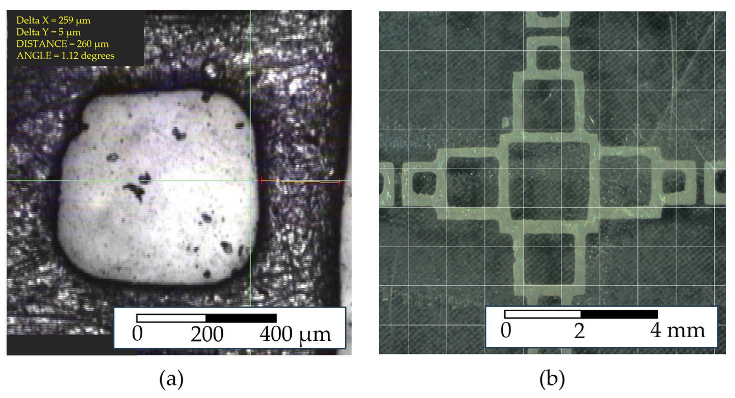
Figure 11a presents a magnified microscopic image to illustrate resolution errors observed in screen printing. Originally, during the design phase, the wire width (w) was intended to be 0.20 mm, but it measured 0.26 mm in the fabricated sample, with the rounding of the square’s corners attributed to resolution limits in the screen-printing process. Figure 11b displays a microscopic image of the entire unit structure. Such discrepancies were anticipated, prompting a parametric study, as demonstrated in Figure 5a. Although variations in wire width (w) influence the resonant frequency and absorption rate, simulations have confirmed that the magnitude of these errors remains within a range that does not significantly impact the performance of the fabricated samples.

3.2. Measured Optical Transparency

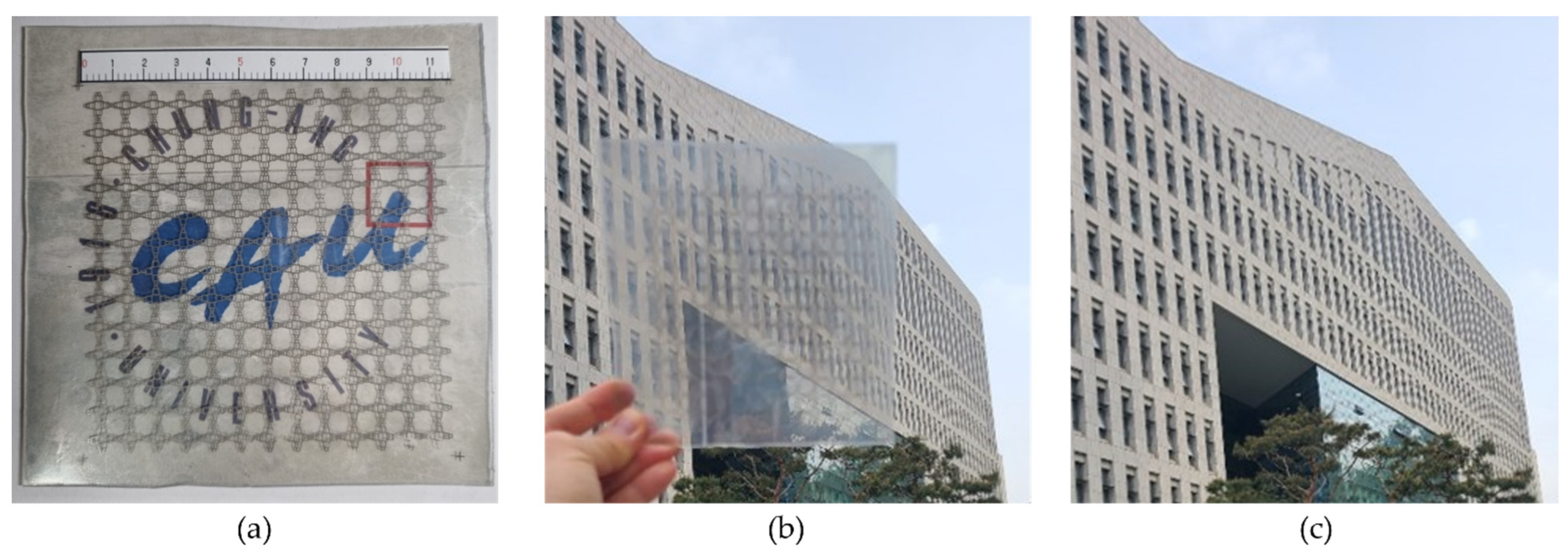
Figure 12 shows the transparency of the fabricated MMA. As shown in Figure 12a, the unit cells were arranged in a 13 × 13 array to implement the entire structure measuring 115.7 × 115.7 mm2. The transparency of the fabricated MMA is such that the logo on the back of the sample is clearly visible to the naked eye. The differences in Figure 12b,c, with and without the fabricated MMA, confirm that the transparency is appropriate for outdoor environments.
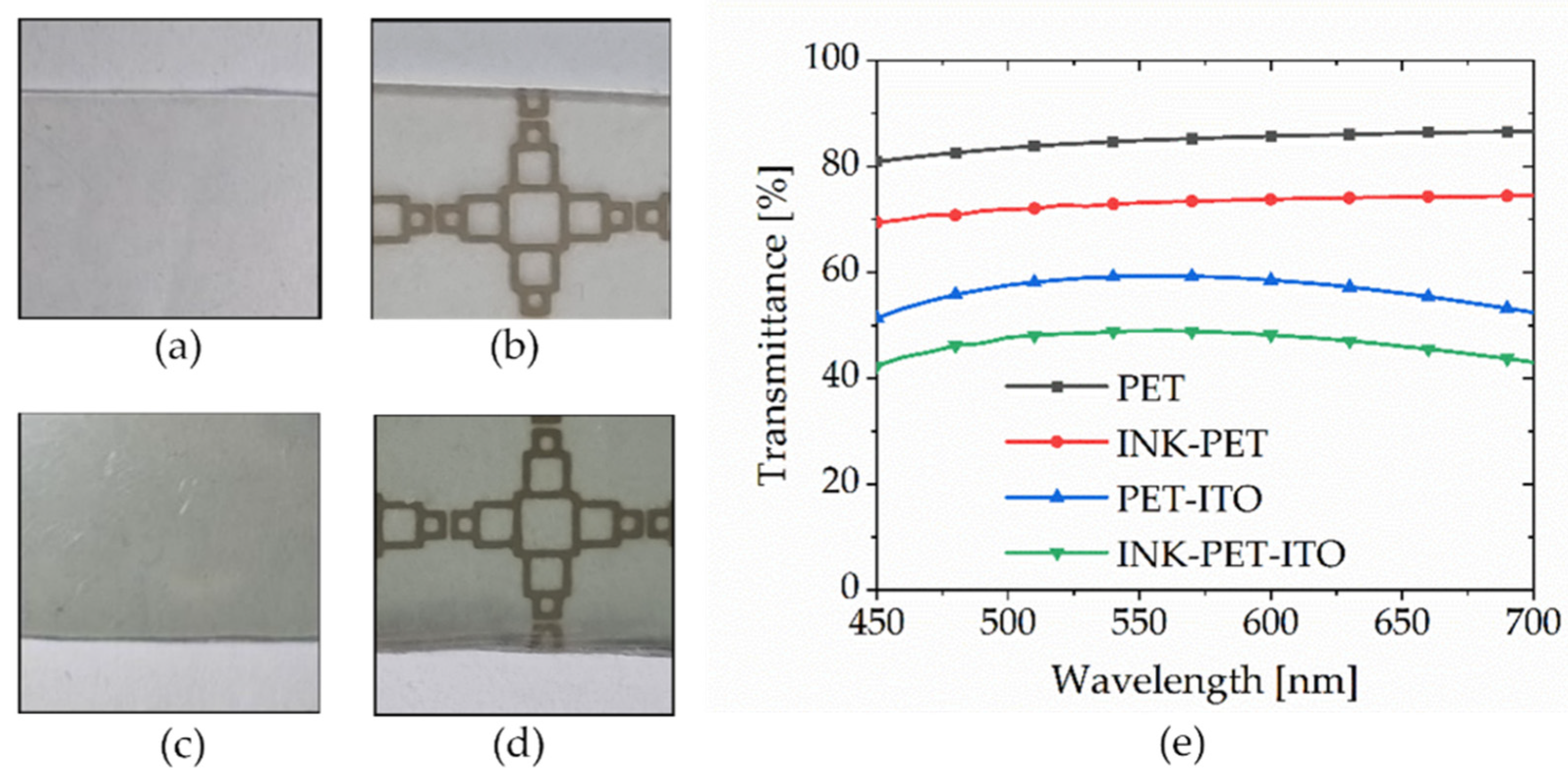
The proposed MMA boasts significant transparency as a performance characteristic. A spectrophotometer (CM-36dG, Konica Minolta, Tokyo, Japan) was used to quantitatively assess this aspect. The metamaterial absorber’s structure consists of three layers, including the top layer ink pattern, the PET substrate in the middle, and the ITO ground plane at the bottom. Optical transmittance across various spectral wavelengths was measured while keeping the substrate constant and varying the presence of the top and bottom layers. Figure 13a,b illustrate configurations without the bottom layer, whereas Figure 13a,c depict examples without the top layer. Figure 13e illustrates the sample’s average transparency, which is 46.70% across the visible light spectrum (450 to 700 nm). The PET substrate alone exhibits 84.12% transparency, whereas PET with an ink pattern exhibits 72.98% transparency, and PET with ITO exhibits 56.69%. Compared PET only, adding layers to either the top or bottom reduces transparency. The presence of ink patterns results in an 86.05% difference in transparency, and the presence or absence of ITO leads to a 66.84% difference in transparency. This highlights the effectiveness of using narrow-area ink patterns in achieving transparency.

3.3. Measured Absorptivity

Figure 14 illustrates the absorption measurement setup designed to validate the performance of the fabricated sample. The sample is positioned in the center of a wedge-shaped absorber, with horn antennas positioned at a distance of 1 m on both sides to satisfy the far-field condition. The corresponding time for this distance is calculated, and the impulse measured using the vector network analyzer (VNA, Anritsu MS2038C) at this time delay is considered the desired signal. All other signals outside this impulse in the time domain are removed, and the data are then transformed into the frequency domain. This method is applied to both a copper plate and air to measure the reflection and transmission coefficients, assuming that the copper plate reflects all signals while air transmits all signals.
F n = n λ d 1 d 2 d 1 + d 2
Equation (8) is employed to calculate Fn, the radius of the nth order Fresnel zone. Where, d1 and d2 denote the distances from each antenna, respectively, and λ represents the wavelength of the target frequency in air [43]. The calculated radius of the first-order Fresnel zone is 122.4 mm, indicating that the test window containing the sample may be insufficiently sized in relation to the Fresnel zone. To mitigate errors caused by the diffraction of electromagnetic waves due to this constrained window and waves reflected from other objects, we utilized a time-gating method [44]. We determined the duration required for electromagnetic waves to travel from the Tx Antenna to the Rx Antenna via the shortest path. Subsequently, employing the time-gating function of the vector network analyzer utilized in our measurements, we excluded all electromagnetic waves that followed paths other than the shortest one.
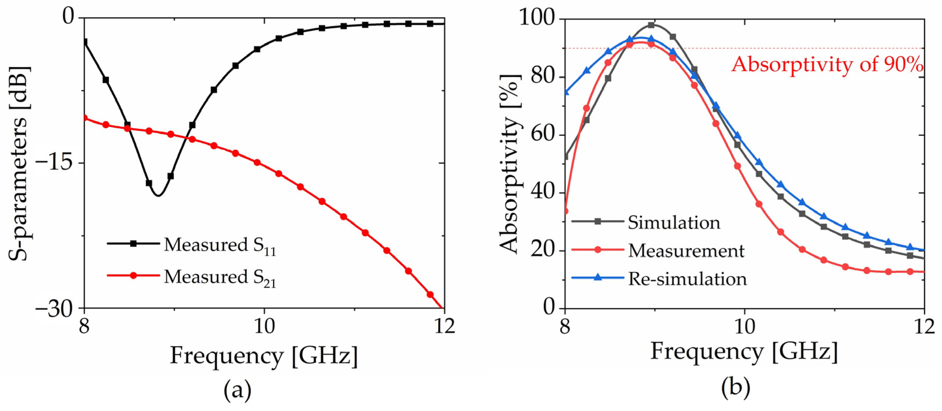
Figure 15a represents the difference in the reflection coefficient between the sample and copper as S11, and the difference in the transmission coefficient between the sample and air as S21, allowing for the removal of environmental effects. The reflection coefficient reaches a peak of −18.39 dB at 8.82 GHz, whereas the transmission coefficient is lower than −10.30 dB in the X-band. The result is subsequently converted back to absorptivity, as demonstrated in Figure 15b, utilizing Equation (1). The measured absorptivity peak was 91.99% at 8.85 GHz, which did not align with the simulation that achieved 98.00% at 8.98 GHz. To reconcile the discrepancies between the initial simulation and the measured values, the sheet resistivity of ITO film in the simulation was adjusted from 7 Ω/sq to 45 Ω/sq. This adjustment effectively brought the simulated results in closer agreement with the measured values.
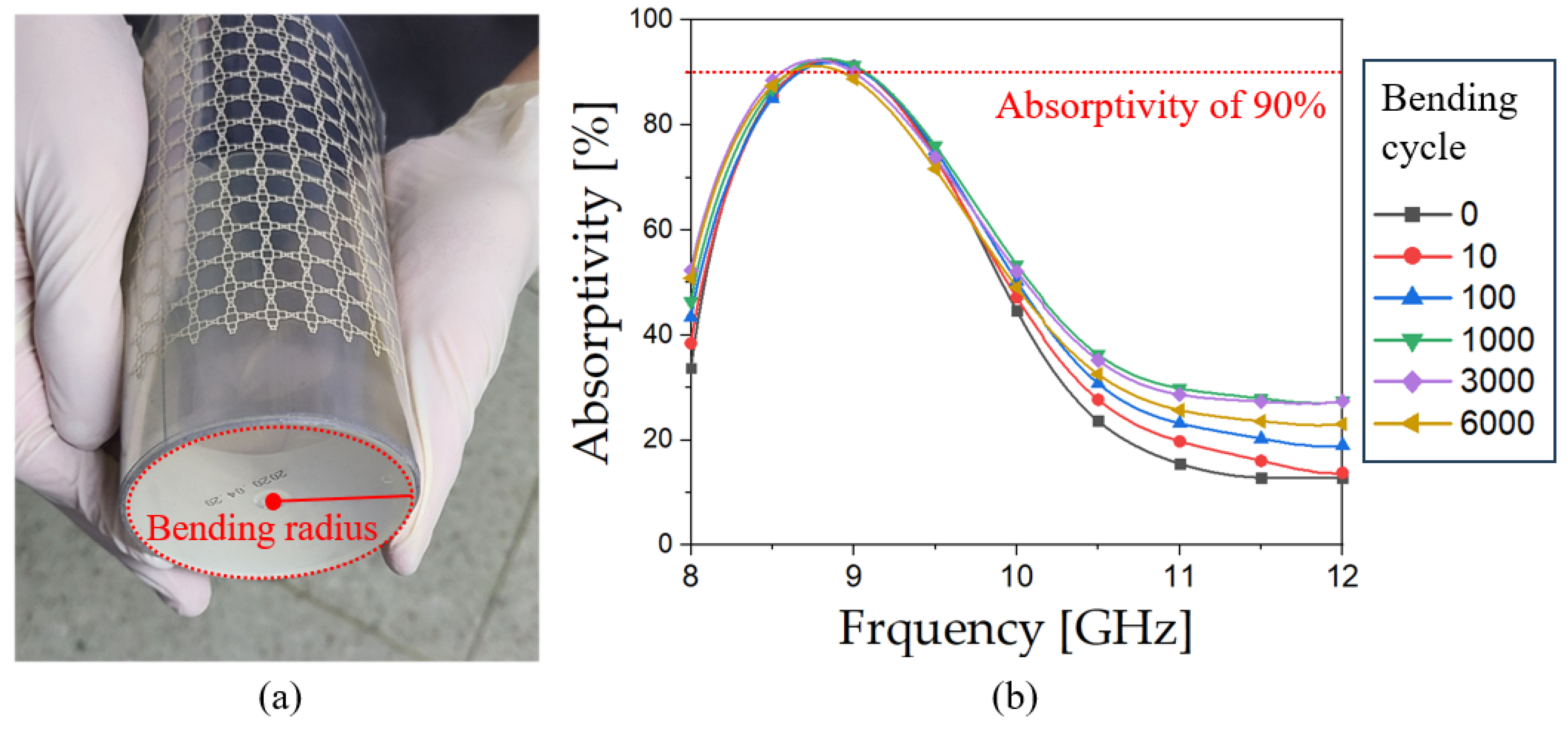
Figure 16 demonstrates the stability of the proposed MMA by evaluating the bending radius limit at which the MMA maintains its performance, as well as illustrating the variation in absorption performance under repeated bending. Specifically, Figure 16a investigates the minimum bending radius required to sustain absorber performance, confirming that the proposed MMA can tolerate bending without functional loss if the bending radius is at least 3.5 cm. Below this threshold, damage to the ITO layer on the ground surface leads to a loss in conductivity. Furthermore, Figure 16b assesses the durability of the proposed MMA by examining the absorption rate variation after more than 6000 bending cycles. The results indicate that the MMA retains over 90% of its electromagnetic wave absorption capacity at the resonant frequency, even after extensive bending. These experimental findings confirm that the proposed MMA not only exhibits significant flexibility but also maintains its performance through numerous bending cycles.
Table 1 compares the proposed MMA with other transparent and flexible MMAs. Although transparent and flexible substrates come in many varieties, incorporating conductive elements remains a challenge. For this comparison, fractional bandwidth was calculated according to the following equation:
F r a c t i o n a l   B a n d w i d t h = f h i g h f l o w f c
where f h i g h and f l o w are the highest and lowest frequencies, respectively. In addition, f c is the center frequency between f h i g h   and f l o w .
On occasion, conductive functionalities are achieved through the use of metal meshes or thin conductive wire structures, although such instances are relatively rare. In the majority of cases, indium tin oxide (ITO) is the preferred material for incorporating conductive properties. However, the choice of substrates and processes that can employ ITO is significantly limited. A common technique involves patterning on PET substrates via laser etching. In contrast, this study employs screen-printing technology, which provides advantages in terms of cost, speed, and scalability for mass production, particularly when compared with laser etching. However, the non-transparent nature of the silver particle ink used for printing and the need to cover the entire plane with ITO for grounding reduce transparency compared with other methods. Despite not being specifically designed for miniaturization, the MMA proposed in this study demonstrates an acceptable unit cell size in contrast to others.

4. Conclusions

In this study, we introduce the use of fractals and metal mesh in the screen-printing fabrication method to produce transparent and flexible MMAs. The proposed MMA comprises a top pattern, substrate, and bottom ground. The unit cell of the top pattern features a fractal structure that begins with a large central square and expands outward with smaller squares in all four directions. The arrangement of this unit cell results in a metal mesh structure, which ensures flexibility and transparency. By increasing the fractal order through simulation, we optimized the resonant frequency for the target X-band, which is a novel approach. Contrary to the prevalent approach in the fabrication of transparent and flexible MMAs, which predominantly employ ITO to create patterns, thus necessitating expensive and complex processes, this study has opted for a screen-printing technique. By employing this method, patterns were printed on PET substrates using silver particle ink, presenting a cost-effective and simpler alternative to the traditional ITO-based process. The fabricated sample demonstrates a peak absorptivity of 91.99% at 8.85 GHz and an overall transparency of 46.70%.

Author Contributions

Conceptualization, S.L.; methodology, S.L.; software, D.L. and J.C.; validation, D.L. and J.C.; formal analysis, J.C.; investigation, J.C. and D.L.; resources, J.C. and D.L.; data curation, J.C. and D.L.; writing—original draft preparation, J.C.; visualization, J.C.; supervision, S.L.; project administration, S.L.; funding acquisition, S.L. All authors have read and agreed to the published version of the manuscript.

Funding

This research was supported by the National Research Foundation of Korea (NRF) grant funded by the Korea government (MSIT) (2021R1A2C3005239) and the MSIT (Ministry of Science and ICT), Korea, under the ITRC (Information Technology Research Center) support program (IITP-2023-RS-2022-00156353) supervised by the IITP (Institute for Information and Communications Technology Planning and Evaluation).

Data Availability Statement

Data are contained within the article.

Conflicts of Interest

The authors declare no conflicts of interest.

References

  1. Rao, G.; Mahulikar, S. Integrated Review of Stealth Technology and Its Role in Airpower. Aeronaut. J. 2002, 106, 629–642. [Google Scholar] [CrossRef]
  2. Le Chevalier, F. Principles of Radar and Sonar Signal Processing, 1st ed.; Artech House: Norwood, MA, USA, 2001. [Google Scholar]
  3. Oh, S.Y.; Cha, K.H.; Hong, H.; Park, H.; Hong, S.K. Measurement of Nonlinear RCS of Electronic Targets for Nonlinear Detection. J. Electromagn. Eng. Sci. 2022, 22, 447–451. [Google Scholar] [CrossRef]
  4. Rogalski, A. History of Infrared Detectors. Opto-Electron. Rev. 2012, 20, 279–308. [Google Scholar] [CrossRef]
  5. Chen, X.; Huang, W.; Zhao, C.; Tian, Y. Rain Detection from X-Band Marine Radar Images: A Support Vector Machine-Based Approach. IEEE Trans. Geosci. Remote Sens. 2019, 58, 2115–2123. [Google Scholar] [CrossRef]
  6. Patel, J.S.; Fioranelli, F.; Anderson, D. Review of Radar Classification and RCS Characterisation Techniques for Small UAVs or Drones. IET Radar Sonar Navig. 2018, 12, 911–919. [Google Scholar] [CrossRef]
  7. Vinoy, K.J.; Jha, R.M. Radar Absorbing Materials: From Theory to Design and Characterization, 1st ed.; Kluwer Academic Publishers: Boston, MA, USA, 1996. [Google Scholar]
  8. Seman, F.C.; Cahill, R. Performance Enhancement of Salisbury Screen Absorber Using Resistively Loaded Spiral FSS. Microw. Opt. Technol. Lett. 2011, 53, 1538–1541. [Google Scholar] [CrossRef]
  9. Reinert, J.; Psilopoulos, J.; Grubert, J.; Jacob, A.F. On the Potential of Graded-Chiral Dallenbach Absorbers. Microw. Opt. Technol. Lett. 2001, 30, 254–257. [Google Scholar] [CrossRef]
  10. Kim, G.; Kim, S.; Lee, B. Design of Wideband Microwave Absorbers Using Reactive Salisbury Screens with Maximum Flat Reflection. J. Electromagn. Eng. Sci. 2019, 19, 71–81. [Google Scholar] [CrossRef]
  11. Choi, W.-H.; Song, W.-H.; Lee, W.-J. Broadband Radar Absorbing Structures with a Practical Approach from Design to Fabrication. J. Electromagn. Eng. Sci. 2020, 20, 254–261. [Google Scholar] [CrossRef]
  12. Ning, J.; Chen, K.; Zhao, W.; Zhao, J.; Jiang, T.; Feng, Y. An Ultrathin Tunable Metamaterial Absorber for Lower Microwave Band Based on Magnetic Nanomaterial. Nanomaterials 2022, 12, 2135. [Google Scholar] [CrossRef]
  13. Suresh Kumar, N.; Naidu, K.C.B.; Banerjee, P.; Anil Babu, T.; Venkata Shiva Reddy, B. A Review on Metamaterials for Device Applications. Crystals 2021, 11, 518. [Google Scholar] [CrossRef]
  14. Sowjanya, A.; Vakula, D. Compact Dual Bandpass Filter Using Dual-Split Ring Resonator for 5G Upper Microwave Flexible Use Services. J. Electromagn. Eng. Sci. 2022, 22, 434–439. [Google Scholar] [CrossRef]
  15. Rhee, J.; Yoo, Y.; Kim, K.; Kim, Y.; Lee, Y. Metamaterial-Based Perfect Absorbers. J. Electromagn. Waves Appl. 2014, 28, 1541–1580. [Google Scholar] [CrossRef]
  16. Landy, N.I.; Sajuyigbe, S.; Mock, J.J.; Smith, D.R.; Padilla, W.J. Perfect Metamaterial Absorber. Phys. Rev. Lett. 2008, 100, 207402. [Google Scholar] [CrossRef] [PubMed]
  17. Min, P.; Song, Z.; Yang, L.; Ralchenko, V.G.; Zhu, J. Optically Transparent Flexible Broadband Metamaterial Absorber Based on Topology Optimization Design. Micromachines 2021, 12, 1419. [Google Scholar] [CrossRef] [PubMed]
  18. Nguyen, T.D.; Lee, Y.; Jung, C.W. Transparent and Flexible Patch Antenna Using MMF for Conformal WiFi-6E Applications. J. Electromagn. Eng. Sci. 2023, 23, 310–317. [Google Scholar] [CrossRef]
  19. Zhang, Y.; Dong, H.; Mou, N.; Li, H.; Yao, X.; Zhang, L. Tunable and Transparent Broadband Metamaterial Absorber with Water-Based Substrate for Optical Window Applications. Nanoscale 2021, 13, 7831–7837. [Google Scholar] [CrossRef]
  20. Park, S.; Shin, G.; Kim, H.; Kim, Y.; Yoon, I.-J. Polarization and Incidence Angle Independent Low-Profile Wideband Metamaterial Electromagnetic Absorber Using Indium Tin Oxide (ITO) film. Appl. Sci. 2021, 11, 9315. [Google Scholar] [CrossRef]
  21. Dong, Y.; Yu, D.; Li, G.; Cao, Y.; Ruan, Y.; Lin, M. Ultrathin and Optically Transparent Microwave Absorber Based on Flexible Silver Nanowire Film. Crystals 2021, 11, 1583. [Google Scholar] [CrossRef]
  22. Chen, J.; Zhao, Y.-T.; Feng, W.; Zhang, Y. Miniaturized metamaterial absorber with high transparency using narrow metallic strip. J. Appl. Phys. 2021, 130, 185107. [Google Scholar] [CrossRef]
  23. Soghi, S.; Heidar, H.; Haraty, M.R.; Nayyeri, V. Single-Layer Broadband Optically Transparent Metamaterial Absorber Using Gold Thin Film. IEEE Trans. Microw. Theory Tech. 2023, 1–10. [Google Scholar] [CrossRef]
  24. Lee, S.; Lee, M.; Lim, S. Frequency Reconfigurable Antenna Actuated by Three-Storey Tower Kirigami. Extrem. Mech. Lett. 2020, 39, 100833. [Google Scholar] [CrossRef]
  25. Abdulkarim, Y.I.; Xiao, M.; Awl, H.N.; Muhammadsharif, F.F.; Lang, T.; Saeed, S.R.; Alkurt, F.Ö.; Bakır, M.; Karaaslan, M.; Dong, J. Simulation and Lithographic Fabrication of a Triple Band Terahertz Metamaterial Absorber Coated on Flexible Polyethylene Terephthalate Substrate. Opt. Mater. Express 2022, 12, 338–359. [Google Scholar] [CrossRef]
  26. Oh, H.-S.; Jeong, S.; Yun, Y.; Jeong, S.Y. Development of Transmission Line Employing Graphene-Silver Nanowire/PET Structure for Application in Flexible and Wearable Devices in X-Band Wireless Communication Systems. J. Korean Inst. Electromagn. Sci. 2024, 24, 1–8. [Google Scholar] [CrossRef]
  27. Kim, H.K.; Ling, K.; Kim, K.; Lim, S. Flexible Inkjet-Printed Metamaterial Absorber for Coating a Cylindrical object. Opt. Express 2015, 23, 5898–5906. [Google Scholar] [CrossRef]
  28. Zhou, Q.; Yin, X.; Ye, F.; Mo, R.; Tang, Z.; Fan, X.; Cheng, L.; Zhang, L. Optically Transparent and Flexible Broadband Microwave Metamaterial Absorber with Sandwich Structure. Appl. Phys. A 2019, 125, 131. [Google Scholar] [CrossRef]
  29. Hyun, W.J.; Secor, E.B.; Hersam, M.C.; Frisbie, C.D.; Francis, L.F. High-Resolution Patterning of Graphene by Screen Printing with a Silicon Stencil for Highly Flexible Printed Electronics. Adv. Mater. 2015, 27, 109–115. [Google Scholar] [CrossRef]
  30. Park, S.; Park, E.; Lee, M.; Lim, S. Shape-Morphing Antenna Array by 4D-Printed Multimaterial Miura Origami. ACS Appl. Mater. Interfaces 2023, 15, 49843–49853. [Google Scholar] [CrossRef]
  31. Lee, D.; Kim, H.K.; Lim, S. Textile Metamaterial Absorber Using Screen Printed Chanel Logo. Microw. Opt. Technol. Lett. 2017, 59, 1424–1427. [Google Scholar] [CrossRef]
  32. Bark, S.; Kim, J.; Lee, M.; Lim, S. Optically Transparent Dual-Band Metamaterial Absorber Using Ag Nanowire Screen-Printed Second-Order Cross-Fractal Structures. Fractal Fract. 2024, 8, 153. [Google Scholar] [CrossRef]
  33. Alsulami, Q.A.; Wageh, S.; Al-Ghamdi, A.A.; Bilal, R.M.H.; Saeed, M.A. A Tunable and Wearable Dual-Band Metamaterial Absorber Based on Polyethylene Terephthalate (PET) Substrate for Sensing Applications. Polymers 2022, 14, 4503. [Google Scholar] [CrossRef] [PubMed]
  34. Dong, J.; Ma, Y.; Wang, M. An Ultra-Wideband Miniaturized Ultrathin Flexible Metamaterial Absorber Using Lightweight ITO Film. IEEE Antennas Wirel. Propag. Lett. 2023, 22, 2970–2974. [Google Scholar] [CrossRef]
  35. Sabban, A. Novel Meta-Fractal Wearable Sensors and Antennas for Medical, Communication, 5G, and IoT Applications. Fractal Fract. 2024, 8, 100. [Google Scholar] [CrossRef]
  36. Vallappil, A.K.; Khawaja, B.A.; Rahim, M.K.A.; Uzair, M.; Jamil, M.; Awais, Q. Minkowski–Sierpinski Fractal Structure-Inspired 2 × 2 Antenna Array for Use in Next-Generation Wireless Systems. Fractal Fract. 2023, 7, 158. [Google Scholar] [CrossRef]
  37. Benkhadda, O.; Saih, M.; Ahmad, S.; Al-Gburi, A.J.A.; Zakaria, Z.; Chaji, K.; Reha, A. A Miniaturized Tri-Wideband Sierpinski Hexagonal-Shaped Fractal Antenna for Wireless Communication Applications. Fractal Fract. 2023, 7, 115. [Google Scholar] [CrossRef]
  38. Bisht, N.; Malik, P.K.; Das, S.; Islam, T.; Asha, S.; Alathbah, M. Design of a Modified MIMO Antenna Based on Tweaked Spherical Fractal Geometry for 5G New Radio (NR) Band N258 (24.25–27.25 GHz) Applications. Fractal Fract. 2023, 7, 718. [Google Scholar] [CrossRef]
  39. Tumakov, D.; Chikrin, D.; Kokunin, P. Miniaturization of a Koch-Type Fractal Antenna for Wi-Fi Applications. Fractal Fract. 2020, 4, 25. [Google Scholar] [CrossRef]
  40. Jeong, H.; Tentzeris, M.M.; Lim, S. Optically Transparent Metamaterial Absorber Using Inkjet Printing Technology. Materials 2019, 12, 3406. [Google Scholar] [CrossRef] [PubMed]
  41. Chaudhary, K.; Singh, G.; Ramkumar, J.; Ramakrishna, S.A.; Srivastava, K.V.; Ramamurthy, P.C. Optically Transparent Protective Coating for ITO-Coated PET-Based Microwave Metamaterial Absorbers. IEEE Trans. Compon. Packag. Manuf. Technol. 2020, 10, 378–388. [Google Scholar] [CrossRef]
  42. Kim, M.; Lee, D.; Oh, Y.; Lee, J.-Y.; Kim, B.; Park, J.; Park, D.; Hong, W. Antenna-on-Display Concept on an Extremely Thin Substrate for Sub-6 GHz Wireless Applications. IEEE Trans. Antennas Propag. 2022, 70, 5929–5934. [Google Scholar] [CrossRef]
  43. Manning, T. Microwave Radio Transmission Design Guide, 2nd ed.; Artech House: Norwood, MA, USA, 2009. [Google Scholar]
  44. Lee, S.; Lee, J. Azimuthal Six-Channel Retrodirective Metagrating. IEEE Trans. Antennas Propag. 2021, 69, 3588–3592. [Google Scholar] [CrossRef]
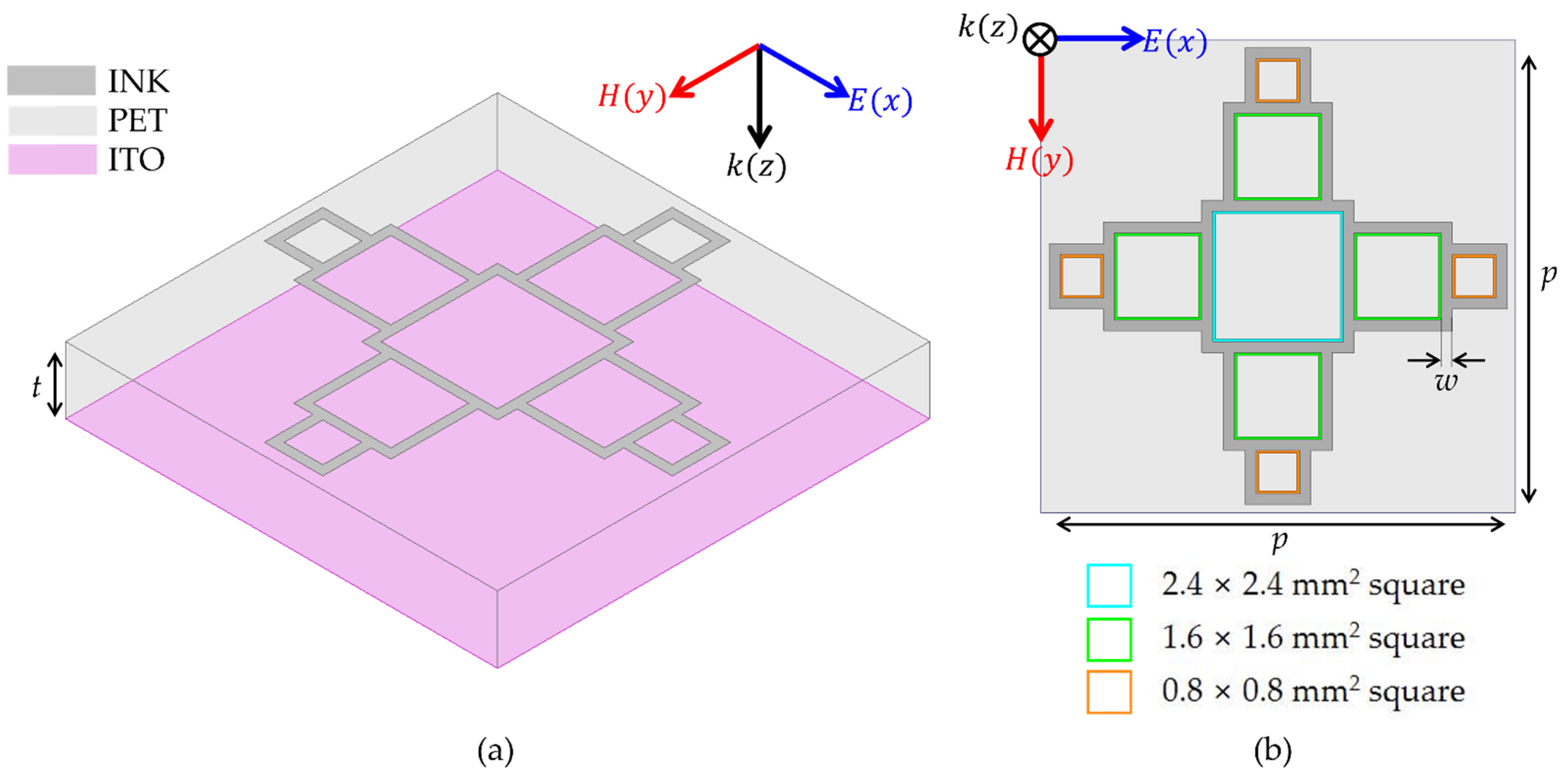
Figure 1. Geometric structure of proposed MMA. (a) perspective view; (b) top view.
Fractalfract 08 00284 g001
Figure 2. (a) Boundary condition of simulation setup; (b) 3D view of metal mesh MMA.
Fractalfract 08 00284 g002
Figure 3. (a) Equivalent circuit modeling; (b) 3D and circuit simulation.
Fractalfract 08 00284 g003
Figure 4. Field simulation. (a) E-field distribution; (b) top surface current distribution; (c) bottom volume current distribution; (d) current distribution side view.
Fractalfract 08 00284 g004
Figure 5. Simulated absorptivity of proposed MMA with variation in (a) wire width, (b) sheet resistance of silver ink, (c) ITO film, (d) substrate thickness, (e) permittivity, and (f) loss tangent.
Fractalfract 08 00284 g005
Figure 6. Simulated reflection coefficient at different iterations of fractal unit cell. (a) Initial design; (b) 1st-order iterative design; (c) 2nd-order iterative design; (d) absorptivity plot.
Fractalfract 08 00284 g006
Figure 7. Comparison between the single-square design and fractal design; (a) layout of the single-square design; (b) layout of the proposed fractal design; (c) simulated reflection coefficients of the single-square design and fractal design.
Fractalfract 08 00284 g007
Figure 8. Simulated absorptivity according to a different (a) incident angle and (b) polarization angle.
Fractalfract 08 00284 g008
Figure 9. Pictures of the fabrication method (a) before printing; (b) after printing; (c) screen frame; (d) squeegee.
Fractalfract 08 00284 g009
Figure 10. Illustration for the laminating method.
Fractalfract 08 00284 g010
Figure 11. (a) High-magnification microscopic image; (b) low-magnification microscopic image.
Fractalfract 08 00284 g011
Figure 12. (a) Photograph of the fabricated MMA. Comparative photographs demonstrating the transparency of the proposed MMA via (b) the image taken with MMA and (c) the image taken without the MMA.
Fractalfract 08 00284 g012
Figure 13. Photograph showing visible transparency of (a) PET, (b) INK-PET, (c) PET-ITO, (d) INK-PET-ITO, and their graph of (e) optical transmittance.
Fractalfract 08 00284 g013
Figure 14. Measurement setup; (a) side view and (b) front view of the measurement setup and (c) comparison of the test window with the 1st-order Fresnel zone.
Fractalfract 08 00284 g014
Figure 15. (a) Measured reflection and transmission coefficients and (b) comparison results with the simulation results.
Fractalfract 08 00284 g015
Figure 16. Flexibility and stability tests; (a) proposed MMA to show the bending radius limit; (b) measurement results of absorptivity variation according to bending cycles.
Fractalfract 08 00284 g016
Table 1. Fabrication method comparison of the proposed MMA with those of others.
Ref.Freq
(GHz)
Fractional
Bandwidth
Size *
0 × λ0)
Thickness
0)
TransparencyFlexibilitySubstrateConductorFabrication
Method
[19]5.8~16.294.55%0.24 × 0.240.100@ 400~800 nmNoPET ITOLaser
etching
PMMA
Water
[23]8.5~23.092.06% 0.18 × 0.180.085@ 400~700 nmNoPolycarbonateGoldDeposition
[34]1.98~25.88171.57%0.06 × 0.060.035N/AYesPETITOLaser
ablation
Air
[25]430, 660,
810
N/A0.11 × 0.110.014N/AYesPETAluminumLitho-
graphic
[28]8.0~18.076.92%0.27 × 0.270.123@ 400~800 nmYesPET ITOLaser
etching
PVC
[17]5.3~15.095.56%0.66 × 0.660.202@ visible bandYesPETITOLaser
ablation
PVCCopperElectro-
plating
This work9.02~9.565.81%0.27 × 0.270.043@ 450~700 nmYesPETSilver
nanoparticle
Screen
printing
ITO
* The wavelength in free space (λ0) is calculated at f l o w .
Disclaimer/Publisher’s Note: The statements, opinions and data contained in all publications are solely those of the individual author(s) and contributor(s) and not of MDPI and/or the editor(s). MDPI and/or the editor(s) disclaim responsibility for any injury to people or property resulting from any ideas, methods, instructions or products referred to in the content.