1. Introduction
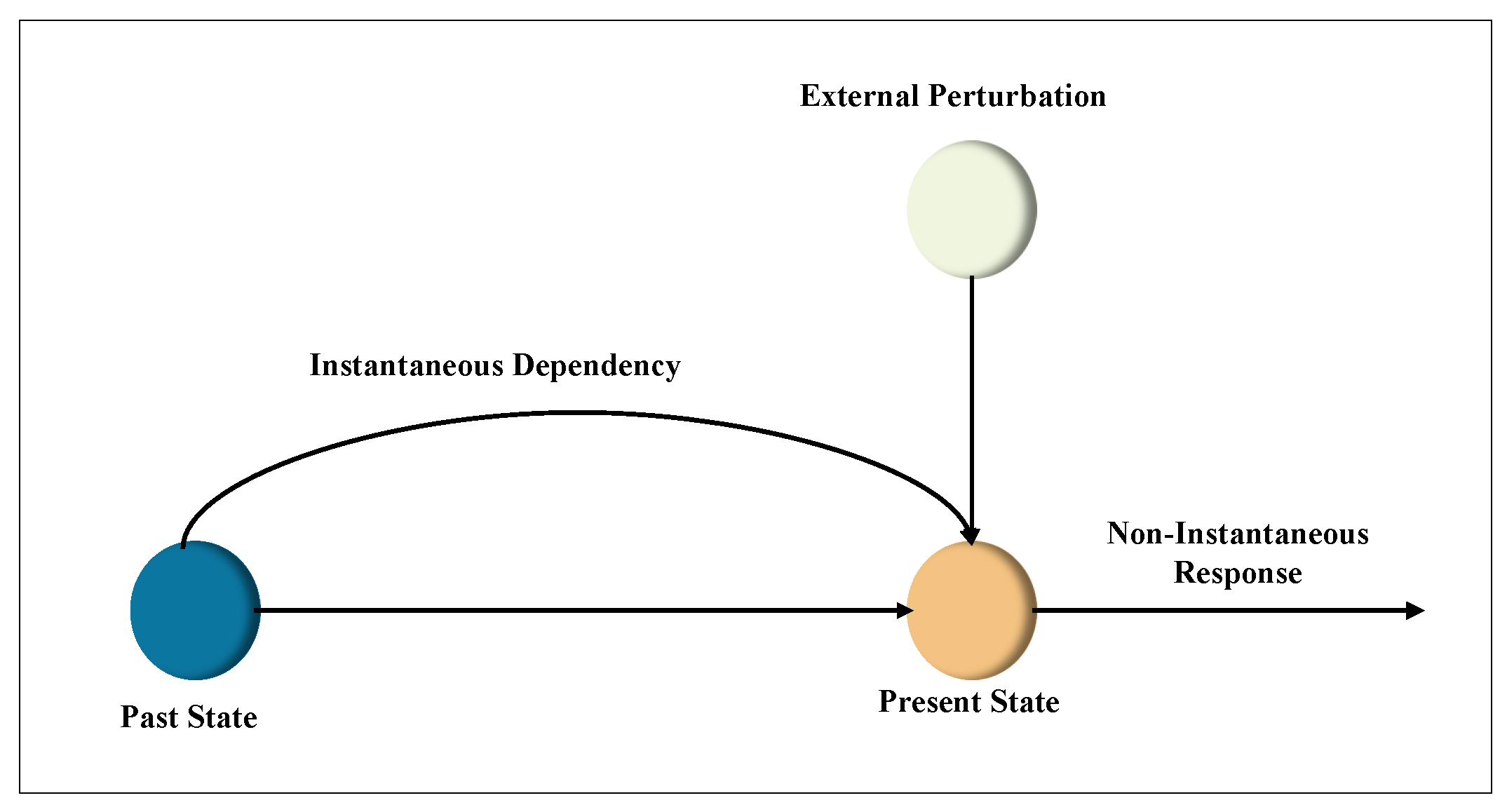
The memory effect is the phenomenon where the present state or response to the stimuli of a system is dependent and affected by the historical conditioning of its dynamic evolution in time. This property has long been studied through the theory of response function across various fields of science and engineering such as physics, biology, and electrical engineering, and it has been observed in most physical systems. For instance, in the context of human cognition, this effect allows humans to recollect past events, learn from past experiences and recognize familiar objects. While many materials, biological organisms and physical systems have exhibited non-instantaneous responses when externally perturbed as illustrated in
Figure 1, the magnitude and degree of memory differ in these systems depending on the specific characteristics and dynamics of the system under consideration. Therefore, memory exhibition would be more experimentally detectable in some physical systems than in others. Consequently, the term “memory” can be defined as the capacity to retain the conditions of a system at a given time and the ability to recall the stored information later [
1]. This phenomenon can be intentionally engineered in certain electronic devices for various scientific and technological applications.
In the mid-19th century, scientists and engineers made pivotal contributions to the development of electrical circuit theories, including the well-known Ohm’s law, formulated by Georg Simon Ohm in 1827. Other notable contributions that laid the groundwork for theoretically understanding the relationships between the fundamental circuit variables, namely, electric current
i, electric voltage
v, electric charge
q, and magnetic flux linkage
, can be attributed to the works of scientists like Michael Faraday, James Clerk Maxwell, and Joseph Henry. Their contributions to circuit theories axiomatically defined how the fundamental two-terminal electronic components behave within electrical circuits analysis in terms of the essential circuit variables. In today’s world, electronic devices are essential to our daily lives, with electrical circuits at their core. The fundamental components of these circuits—resistors, capacitors, and inductors— are instrumental in driving technological progress across diverse disciplines. However, as technology continues to advance at a rapid pace, new non-linear components exhibiting time non-locality have emerged [
2]. This ongoing evolution of both analog and digital circuit components has led to a wide range of applications and has significantly contributed to advancing the frontiers of global technology.
Although the relationships between the four fundamental circuit variables have been mathematically formulated and established by traditional electronic elements along with many other electronic components such as transistors and diode, there was no two-terminal electronic device that could singularly relate the electric charge
q with the flux linkage
until the discovery of the memristor by Leon Chau in 1971 [
3]. The notion of the memristor was predicted when Chau was examining the internal states of non-linear circuits using theoretical analysis and circuitry approaches. He discovered that there was a missing device that should complete the interconnections of the foundational set of core electrical variables. Hence, he proposed the memristor as the quad fundamental device among the league of well-known essential circuit elements. The memristor postulation is revolutionizing the scientific understanding of electrical circuits and devices, and its influence has opened new dimensions to the field of electronics and electrical engineering [
4].
Di Ventra and Pershin, in their collaboration with Leon Chua [
5], characterized the memristor as a non-linear two-terminal electronic component distinguished by its non-volatility and passivity with relatively detectable magnitude of memory. The research shows that if a periodic current or voltage is applied at the input terminal of a memristor, it will exhibit a pinched hysteresis loop (PHL) when the constitutive state variables, namely, current
i and voltage
v, are simultaneously measured and plotted on the
plane. The hysteresis property of the memristor is indicative of the variability in resistance due to its dependence on the history of excitation current or voltage that has passed through the device [
6]. This remarkable property sparked interest among researchers and industry professionals, leading to its first physical realization by HP Lab in 2008. The breakthrough device used deposits of titanium dioxide (TiO
2) sandwiched between two electrodes of platinum with its switching mechanism identified to exhibit the synaptic-like behaviors of those of a neuron in the brain [
7]. The memristor’s ability to change its resistance in response to inputs makes it a promising component for future electronic technologies.
Following the postulation of the memristor, researchers generalized its theoretical basis to encompass memristive systems, and subsequently extended it to include memory capacitive and inductive systems [
8]. This development led to the classification of memcapacitors and meminductors as fundamental electronic elements, which established the relationships between flux linkage
and the time integral of charge
, as well as between electric charge
q and the time integral of flux
, respectively, as shown in
Figure 2. While memristors cannot store energy like memcapacitors and meminductors, all three share similar internal behaviors within their respective systems. Memelements have been identified as potentially applicable in various fields such as neuromorphic computing [
9,
10,
11,
12,
13], chaotic systems [
14,
15,
16,
17], signal processing [
18], memory devices development [
19], quantum computing [
20], stochastic computing [
21,
22], reservoir computing [
23], intelligent computing [
24,
25], in-memory computing [
26], green devices development [
27], and bio-inspired computing applications [
28,
29,
30].
Since the conceptualization of memelements, scientists and engineers have been actively working on developing solid-state versions that align with theoretical models and established characterizations. Despite the complexity of fabricating these elements, their intrinsic value is crucial for scaling technology to new heights. Notable solid-state models developed over the years include the HP memristor, a biomimetic membrane memcapacitor [
31], a metal-oxide memcapacitor [
32], and a meminductor reported in reference [
33]. Nevertheless, the commercialization of the nanoscale devices has faced significant challenges, primarily due to difficulties in fabrication and the lack of suitable semiconductors that can support their practical and scalable development. The precision required at the nanoscale level makes mass production challenging, and issues like device variability, stability, and integration with existing semiconductor technology have slowed down the commercialization process. Therefore, to facilitate studies and applications of these devices in practical scenarios, there is a need to develop circuits that can mimic the functionalities of the solid-state devices. These types of electronic circuits, known as emulator circuits [
34], serve as critical innovations that bridge the gap between theoretical models of electronic devices and their eventual commercial realization as ideal physical devices.
Among the state-of-the-art memristor emulators described in the literature is the grounded flux-controlled (voltage-controlled) memristor introduced in [
35]. This emulator, capable of functioning in both incremental and decremental modes, operates at input frequencies up to 100 MHz. It is built using a distributed voltage and current control (DVCC) component, three PMOS transistors, and a single capacitor. Additionally, reference [
36] proposes a novel voltage-controlled memristor that operates over a wide frequency range from 30 kHz to 120 kHz. The memristor uses a Dual Z output Voltage Dependent Transconductance Amplifier in its architecture to modulate the memristance based on the input voltage. This adjustable memristor design eliminates the need for supplementary analog multipliers commonly found in other memristor emulators. It also uses fewer active and passive elements, offering a significant advantage over many existing emulator circuits. Many other memristor emulators can be found in references [
37,
38,
39].
Memcapacitive behavior has been demonstrated in various materials, including metal-oxide thin films, organic semiconductors, and graphene. A generalized physical structure of a memcapacitor is detailed in reference [
32]. Furthermore, micro-electromechanical systems (MEMS) have been proposed as memcapacitive devices [
19,
40], with one design featuring the replacement of a parallel-plate capacitor electrode with an elastic membrane. This modification enables variable capacitance and switching behavior within the device. Additionally, several emulation circuit models have been developed to showcase the potential applications of memcapacitors in signal processing, memory devices, and neuromorphic computing [
41,
42,
43]. Notably, the emulator model presented in [
43] employs a memristor design that uses a Voltage Differencing Current Conveyor (VDCC) for the adjustment of the memristor’s resistance based on the applied voltage, highlighting its adaptability and effectiveness in various applications.
Recently, in [
44], researchers experimentally demonstrated a physical meminductor exhibiting pinched hysteresis. This model uses platinum thin films influenced by the spin Hall magnetoresistance effect at room temperature. Furthermore, another solid-state meminductor based on TiO2 was reported by the authors in [
45]. However, several of the solid-state devices described in the literature have faced scrutiny regarding their consistency with the established theoretical frameworks, warranting further investigation to validate their behavior for exploring potential applications [
46]. Moreover, the complexity of fabricating these solid-state devices poses significant challenges for commercialization, underscoring the need for emulator circuits for practical experimentation and implementation. Some of the most advanced emulators are documented in references [
47,
48,
49,
50,
51]. For instance, the meminductor emulator developed in [
47], known as a transformer memristor modeled after the HP memristor, simulates meminductive behavior through a defined functional relationship between magnetic flux
and electric current
i. Another model, described in [
48], modifies Antoniou’s gyrator to emulate the behavior of a flux-controlled meminductor without relying on a memristor or inductor. Instead, it operates based on the impedance at the device’s input terminal.
Fractional-order models of memelements provide a higher degree of freedom compared to their integer-order counterparts, as they account for a continuous spectrum of memory and inherently reference historical states of the device, enabling a more nuanced and accurate representation of the physical systems which allows for a dynamic response that reflects both current and past inputs [
52]. This characteristic is particularly advantageous in applications requiring precise control and adaptation to complex environments, such as in neuromorphic computing, signal processing, and advanced memory devices. Fractional-order systems, in general, model a wide range of physical phenomena, from biological and mechanical behaviors to political, economic, ecological, geophysical, chemical, and biochemical processes. By utilizing fractional calculus—a mathematical tool with origins dating back to 1695, first mentioned in a correspondence between Leibniz and L’Hospital [
53]—fractional-order systems achieve a greater precision and flexibility in capturing the intricacies of these complex phenomena. As research continues to evolve, the fractional-order modeling of memelements is expected to play a pivotal role in the next generation of electronic devices by offering new capabilities in areas such as artificial intelligence, quantum computing, and beyond.
Fractional-order memory element (FOME) emulation has been explored previously, but most works focus on analog circuit implementations or specific types of FOMEs. The digital implementations of FOMEs has not been widely addressed. Despite this limited exploration of digital-based FOME emulator implementations, there are notable contributions in the literature. The first relevant work introduced in [
54] explores the conceptualization and FPGA implementation of discrete fractional-order memristor models and memristive systems using Caputo and Grünwald–Letnikov (GL) fractional difference equations. The study also demonstrates a short-term memory effect in the FOME compared to the integer-order memristor, which contributes to more efficient hardware realization. The second study discussed in [
55] presents a novel hardware architecture that can simultaneously configure multiple GL fractional derivative algorithms to construct a fractional-order memristor emulator and its inverse type. This emulator specifically employs the fixed window length algorithm, which uses a certain number of past values (the “window”) to compute the fractional derivative, as well as the K-piecewise linear function, which approximates the fractional derivative by breaking the input signal into segments of linear functions. In this study, which serves as both a theoretical exploration and a call for future research in the area of FOME implementation, we introduce digital fractional-order memelement (DFOME) look-up table-based emulators controlled by voltage sources. The design is based on the model presented in [
56] which features a universal topology applicable to memristors, memcapacitors, and meminductors. The FOME in its analog form consists of a fractional-order capacitor (FOC) proposed by Valsa [
57], four operational amplifiers (AD844) that function as both a current conveyor and a voltage follower, one analog multiplier (AD633), and three additional passive components. Our development methodology involves initially simulating the memelements in MATLAB-Simulink to validate the model’s accuracy. Subsequently, we digitally designed the models using System Generator for DSP. Thereafter, we performed resource and timing analyses of each design and then synthesized the designs on the Artix-7 AC701 evaluation FPGA board.
The motivation behind the development of the memelements are the well-known advantages that digital systems have over their analog counterparts, namely, determinism, accuracy and precision, programmability, speedup, power reduction, and seamless integration with computers [
58]. Therefore, the integral contributions of this work are highlighted as follows:
- (i)
The low-cost FPGA realization of the fractional-order memristor, memcapacitor, and meminductor designed using VHDL blocks of Xilinx System Generator for DSP. The design can achieve the theoretical behaviors of memelements including PHL, which can be enhanced by lowering the fractional orders in high-excitation frequencies.
- (ii)
A demonstration of the JTAG hardware co-simulation of the design showing real-time testing of the memelement-based systems as well as behavioral HDL netlist tests. The results of the hardware experiments are in close alignment with the numerical results from Matlab.
The remainder of the paper is organized in the following way:
Section 2 describes the mathematical modeling of the emulator circuits. Moving on to
Section 3, we present the digital architectural designs of the memelements inclusive of the hardware co-simulation designs.
Section 4 then highlights the results of the experimental test carried out to validate the correctness of the models. We discuss the results in
Section 5 and finally conclude the paper in
Section 6.
2. Mathematical Models of Universal Emulators for Memelements
In this section, we describe the theoretical background of memelements and the mathematical models of FOME designed in this paper. We shall refer the readers of this paper to the detailed formulation of the mathematical models of the memelements emulator topologies adopted in this work, which can be found in reference [
56]. A brief description of the generalized definition and the specific mathematical models of the emulators is hereby presented.
Generally, the mathematical relationship that defines a
u-controlled integer-order memelement with a set of
n state variables denoted as
x at any time
t is expressed in Equations (
1) and (
2):
where
and
denote the output and input of the memelement, respectively,
f is the generalized response of the system, and
g is a continuous vector-valued function in
n-dimensional space [
5].
In a charge-controlled memelement, the state of the device primarily depends on the cumulative electric charge
q that has flowed through it. This charge–flow relationship is linked to the magnetic flux
through the integral of voltage with respect to time
t. In contrast, for voltage-controlled memelements, the controlling state variable is the voltage
v across the device which is related to the rate of change of charge
q. The ideal relationship that governs the operation of a voltage-controlled memristor is expressed by Equation (
3) together with the state equation described in (
2), where the input is the applied voltage, and
G is the memductance of the device:
and for an ideal voltage-controlled memcapacitor, the mathematical representation relating the electric charge to the voltage across the system is given by Equation (
4), where
C is the memcapacitance, which is dependent on the voltage applied across the terminals of the device. The dynamic state behavior of such a memcapacitive device is described by (
2), where
is the applied voltage:
and similarly, Equations (
2) and (
5) define the functional dynamic relationship between the electric current and flux linkage of a generalized flux-controlled meminductor,
where
is the inverse meminductance and
represents the flux
. The specific mathematical models of the universal memelement emulators designed in this work are given as follows:
Fractional-order memristor (FOMR)
The
relationship that describes the FOMR emulator is given as Equation (
6),
where
is the memconductance of the FOMR,
and
represent the input current and input voltage across the FOMR, respectively,
is the fractional integral of the input voltage,
is the value of the FOC utilized in the design, and
is the port voltage of the
terminal of the AD633 multiplier utilized, while
are the resistors.
Fractional-order Memcapacitor (FOMC)
The
relationship that describes the FOMC emulator is given as Equation (
7),
where
is the memcapacitance of FOMC,
is a capacitor, and
represents the charge across FOMC.
Fractional-order Meminductor (FOMI)
The
relationship that describes the FOMI emulator is given as Equation (
8),
where
is the inverse meminductance of the FOMI,
is an inductor, and
represents the flux across the FOMI.
Characteristics of Memelements
The three memelements discussed above have two major fingerprints—characteristics that establish a relationship between their input and output signals based on the governing principle that defines them. These two fingerprints are a result of the physical mechanisms underlying the behavior of a memristors, memcapacitors, and meminductors:
- (1)
For a continuous periodic current or voltage input, the memdevices exhibit a pinched hysteresis loop at the associative state variable origin:
in the case of a memristor,
in the case of a memcapacitor, and
in the case of a meminductor.
- (2)
At increased frequency of the input voltage or current, the pinched hysteresis collapses and tends towards linearity, demonstrating the behavior of a linear resistor, capacitor, and inductor in each case.
3. Design of FOME
In this section, we introduce the designs of the digital emulator circuits, modeled after the equations governing the voltage-controlled FOME. The process involves designing a mapping of the continuous-time behavior of the memelements to their discrete-time representations. This mapping was achieved by developing the digital architecture of each memelement using the Xilinx DSP block set through the System Generator. Subsequently, we compiled and implemented the designs at the hardware level with JTAG co-simulation using Xilinx Artix-7 AC701 Evaluation kit (Telecommunication Laboratory of Instituto Politécnico Nacional, IPN-CITEDI in Tijuana, Baja California, Mexico).
FOMR:
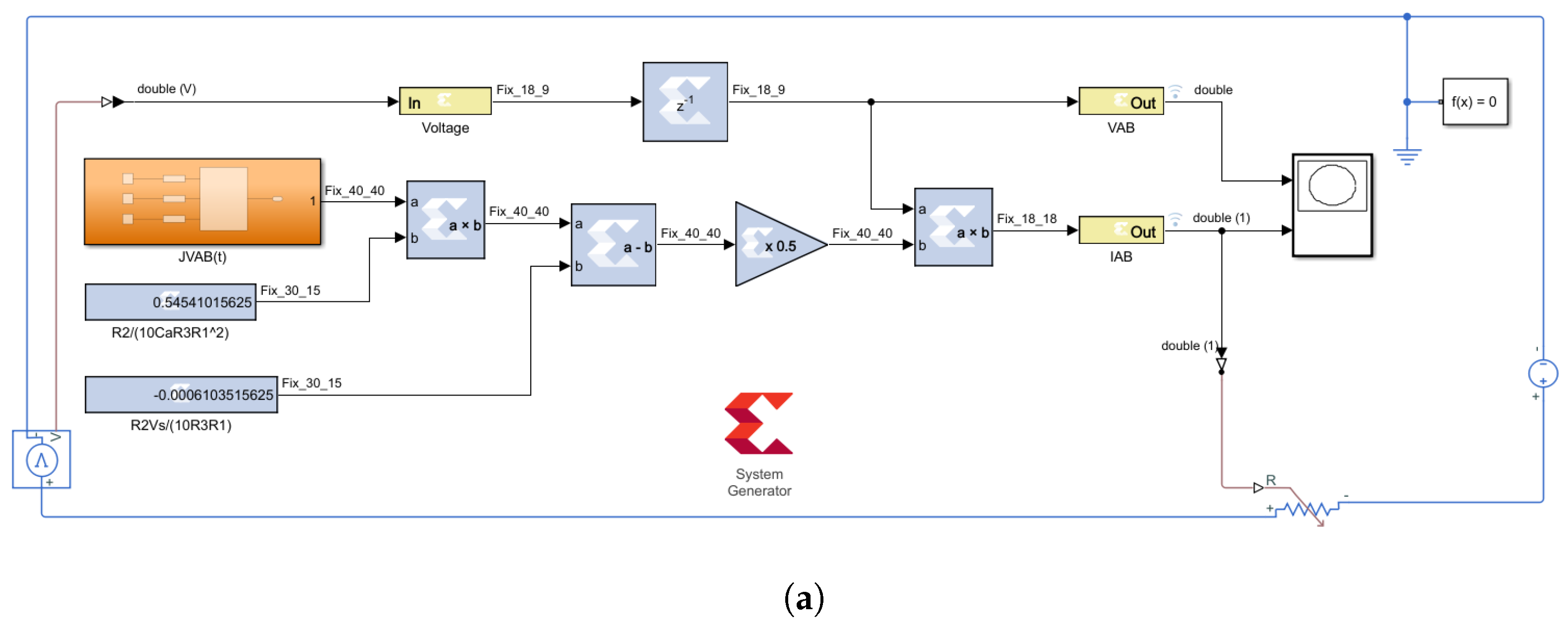
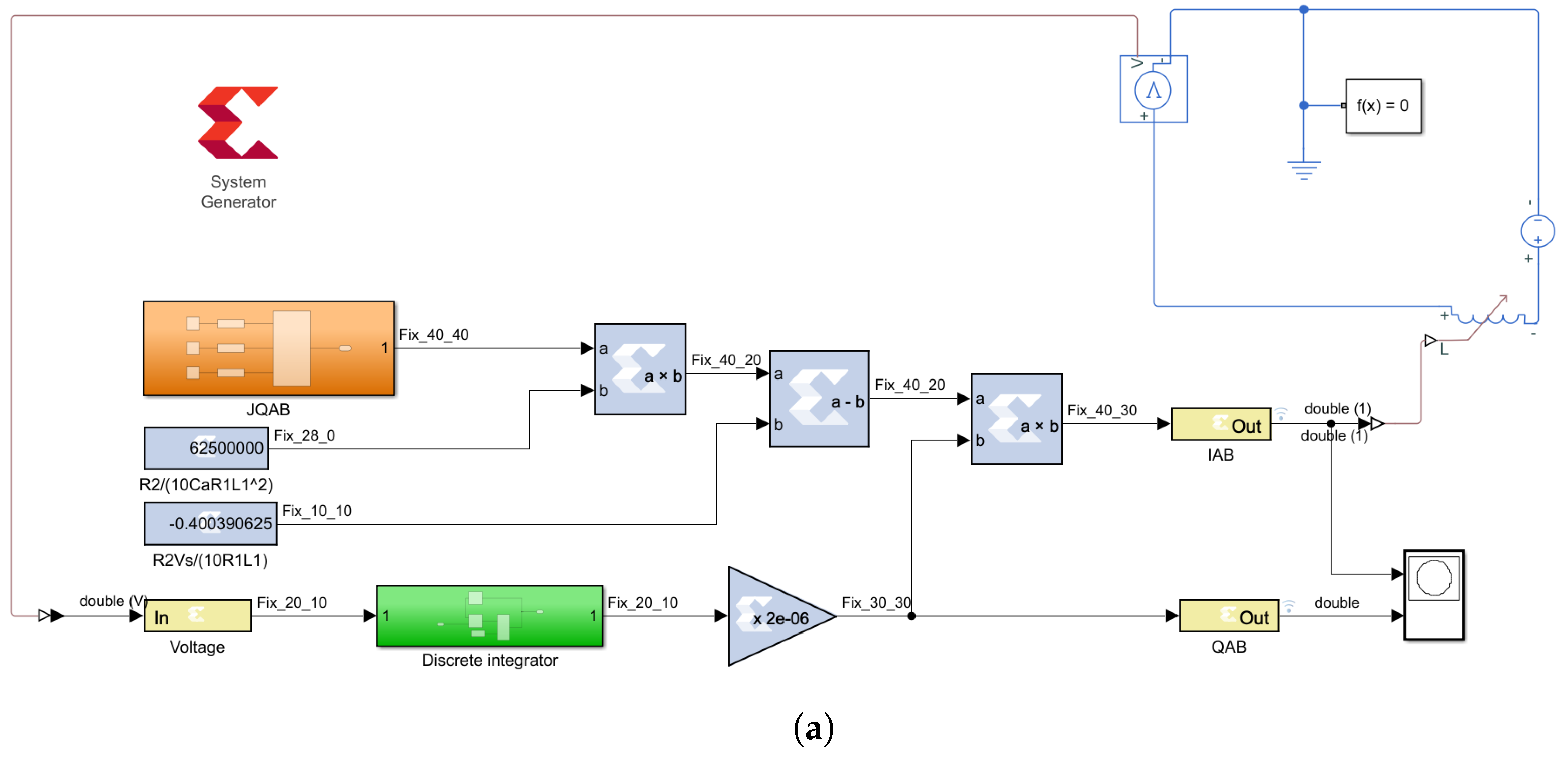
Figure 3a presents the discrete-time model design of the FOMR emulator corresponding to Equation (
6). The design comprises two multiplier blocks, a subtraction block, two constant blocks, a gain block, a delay block, and Simscape components.
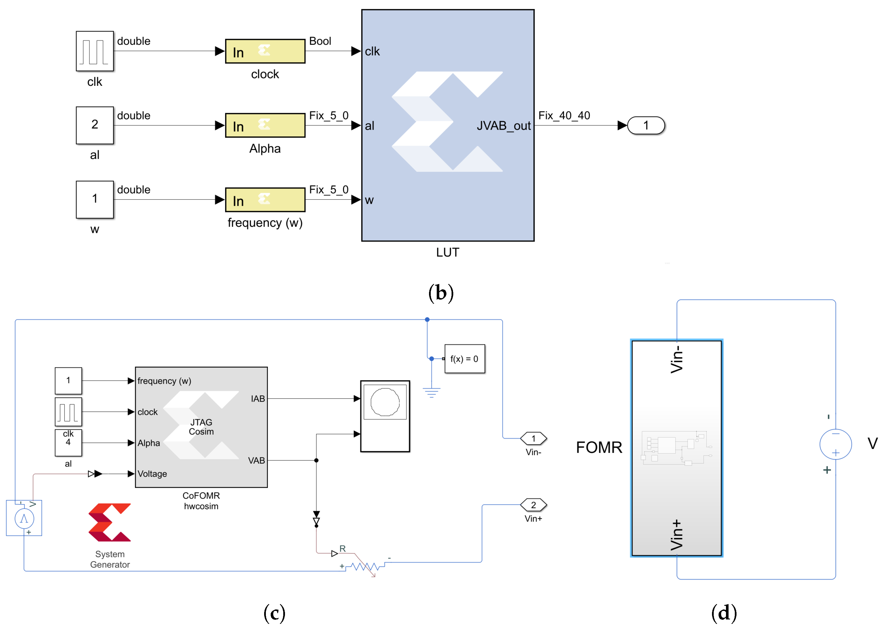
Figure 3b illustrates the configuration of the fractional-order integral (FOI)
of the sinusoidal input voltage
in its steady-state response as mathematically described in Equation (
9). This configuration was implemented in Vivado using a 40-bit lookup table (LUT) computed in MATLAB. The pairs (
) represent the input for the multiplexer selector, allowing for the selection of fractional-order integral values of the input voltage with respect to time.
Figure 3c shows the corresponding JTAG hardware co-simulation block compiled and generated from the design in
Figure 3a and evaluated with a continuous-time voltage source as shown in
Figure 3d:
FOMC:
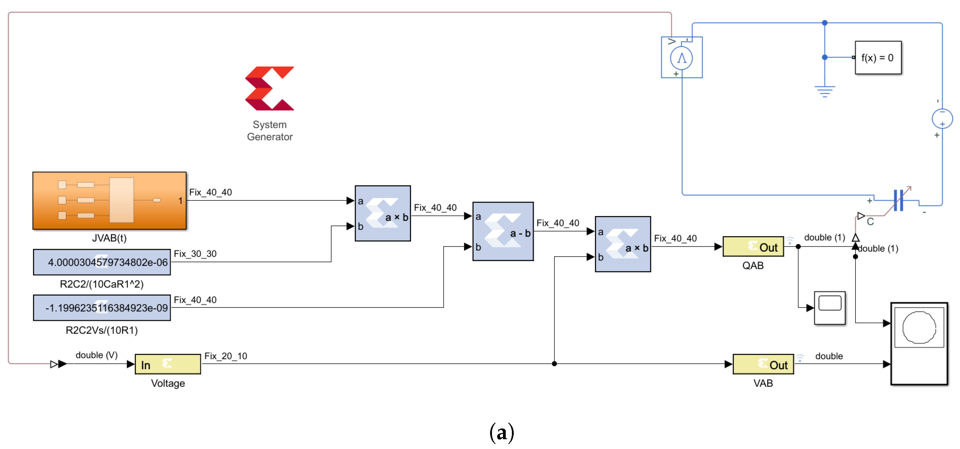
We translated the model of the FOMC described by Equation (
7) into the digital domain using the Xilinx System Generator block set as illustrated in
Figure 4a below. The FOMC emulator design closely resembles the FOMR emulator, which features a fractional-order integral of the driving input voltage in its steady-state as described in Equation (
9). The output of the integral configured using LUT with similar architecture to the FOI design shown in
Figure 3b is determined by the pair (
), which represents the parameters to select the fractional integral operation of the input voltage across the memcapacitor. The complete configuration in
Figure 4a of the memcapacitor design also includes two constant blocks to provide the fixed parameters of the memcapacitor, a multiplier for executing the multiplication operation within the system, a subtraction block, and a gain block that scales the signal as required.
Figure 4b,c show the JTAG hardware co-simulation block of the FOMC design and its evaluation with a voltage source, respectively.
FOMI:
Figure 5a shows the FOMI emulator corresponding to the mathematical model in Equation (
8). The design comprises a subsystem representing a digital integer-order integrator as shown in
Figure 5b which processes the input signal by accumulating the voltage, along with the FOI of the total flux
across the terminals of the meminductor in its steady-state response as described in Equations (
10) and (
11),
where
V is the driving voltage of the meminductor.
is similarly designed using the LUT configuration in
Figure 3b. The complete design also includes two constant blocks, two multipliers, one subtraction block, and a gain block for scaling the output signal from the discrete integrator.
Figure 5c,d show the compiled hardware co-simulation block and an evaluation using a voltage source, respectively.
Samples Stored as LUT and Frequency Impact
First, the values of the LUT for five different combinations of the fractional order (
) and frequency (
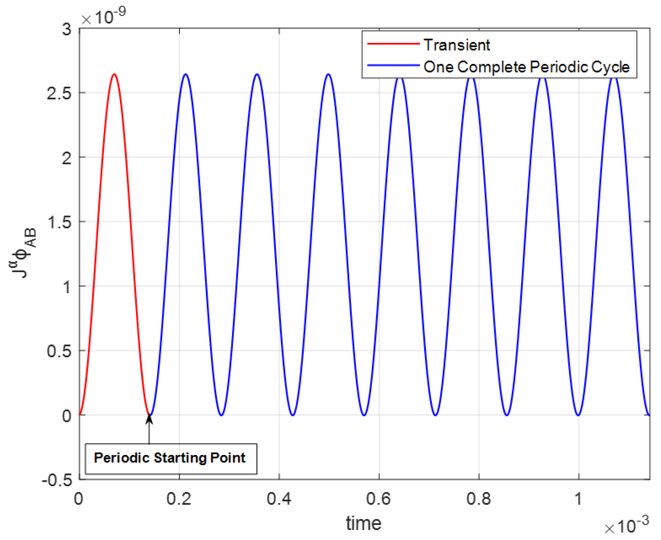
) are computed in Matlab for all the memelements. Next, the values are stored as 40-bit lookup tables (LUTs) in Vivado, which are internally reset to the periodic starting point after a complete stable cycle as illustrated in
Figure 6 for the parameters
kHz,
= 0.95,
and step size of
. The number of samples required to complete one cycle of the waveform in the LUT is fundamentally linked to the signal frequency and the sampling rate. According to the Nyquist theorem, the sampling rate should be at least twice the highest frequency present in the signal. However, to ensure better fidelity, a higher sampling rate is typically used [
59]. For the frequency
kHz, the period
T can be calculated as
, with the sampling rate
of 1 MHz, and the number of samples
N required for one complete cycle can be calculated as
143 samples per cycles. Since the FOIs of the input signals at steady-state response contain the periodic term
) and the constant
, it is expected that the signals will be periodic with the period of
and periodic starting points
for
. However, it is important to mention that there were variations in the calculated data for each cycle in each of the FOI signals, which were identified to have risen from the transient effect or numerical inaccuracies that are inherent in computational simulations. To address this, we stored multiple cycles in the LUTs, specifically eight cycles for the parameter pair
, where the first cycle was considered transient as shown in
Figure 6. This strategy helps to mitigate variations in the LUT values and provide a more consistent representation of the steady-state behavior of the system. Although storing multiple cycles increases the memory requirement of the LUT, this trade-off is justified by the gain in accuracy and stability of the system.
4. Experimental Test Results
In this section, we present the simulation results from Matlab and hardware co-simulation of the FPGA designs, along with a detailed timing and resource analysis of the implemented memelements emulators. We also discuss the impact of system parameters () on the PHL lobe area, and how these parameters influence the performance of the emulators. Moreover, we examine the stability of the designs under varying conditions by measuring the actual output signals on a physical oscilloscope and verifying the consistency with established theoretical characteristics and simulations.
FOMR Fingerprint
To evaluate the functionality of the FOMR emulator described in previous sections, we applied a
sinusoidal input voltage
at the input terminal of the memristor under varying frequency and fractional-order parameter. The system parameters are as follows:
= 10 kΩ,
= 100 kΩ,
= 10 kΩ,
= 18.335
, and
= −6 V for fractional-order values
0.90 and
= 0.95, as well as excitation frequencies
0.4 kHz, 0.8 kHz, and 1.2 kHz. As shown in
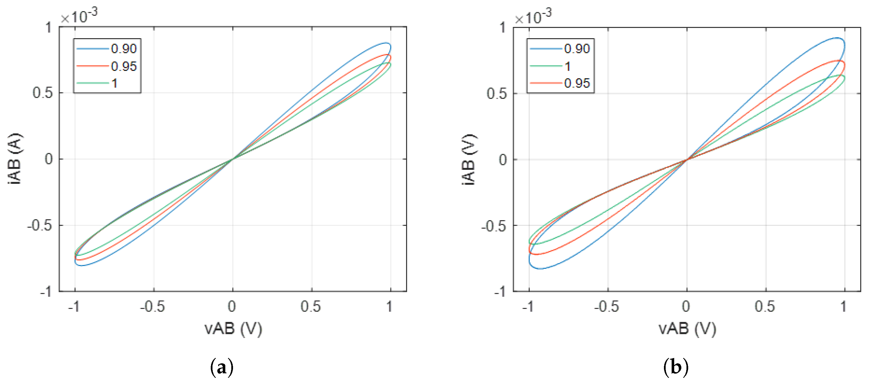
Figure 7a,b, the increase in frequency causes the lobe area of the hysteresis loop to gradually collapse and tend towards linearity. Additionally, it is also observed that when the fractional order of the emulator increases at a constant frequency, the hysteresis also collapses as shown in
Figure 8a,b. This observation suggests that in high-frequency applications where the expanded hysteresis loop is important, reducing the fractional order of the emulator can contribute to enhancing and achieving the desirable property of the memristor.
FOMC Fingerprint
Similarly, we tested the performance of the FOMC emulator developed in this work with a sinusoidal input voltage
with an amplitude of 1 V. The periodic input voltage modulates the memcapacitor’s capacitance and drives the memelement using the following parameters:
= 50 kΩ,
= 100 kΩ,
= 1
,
,
= −6 V. We tested the emulator across fractional-order values
= 0.90 and
= 0.95 under diverse driving frequencies
f = 1.5 kHz, 2.0 kHz, and 2.5 kHz.
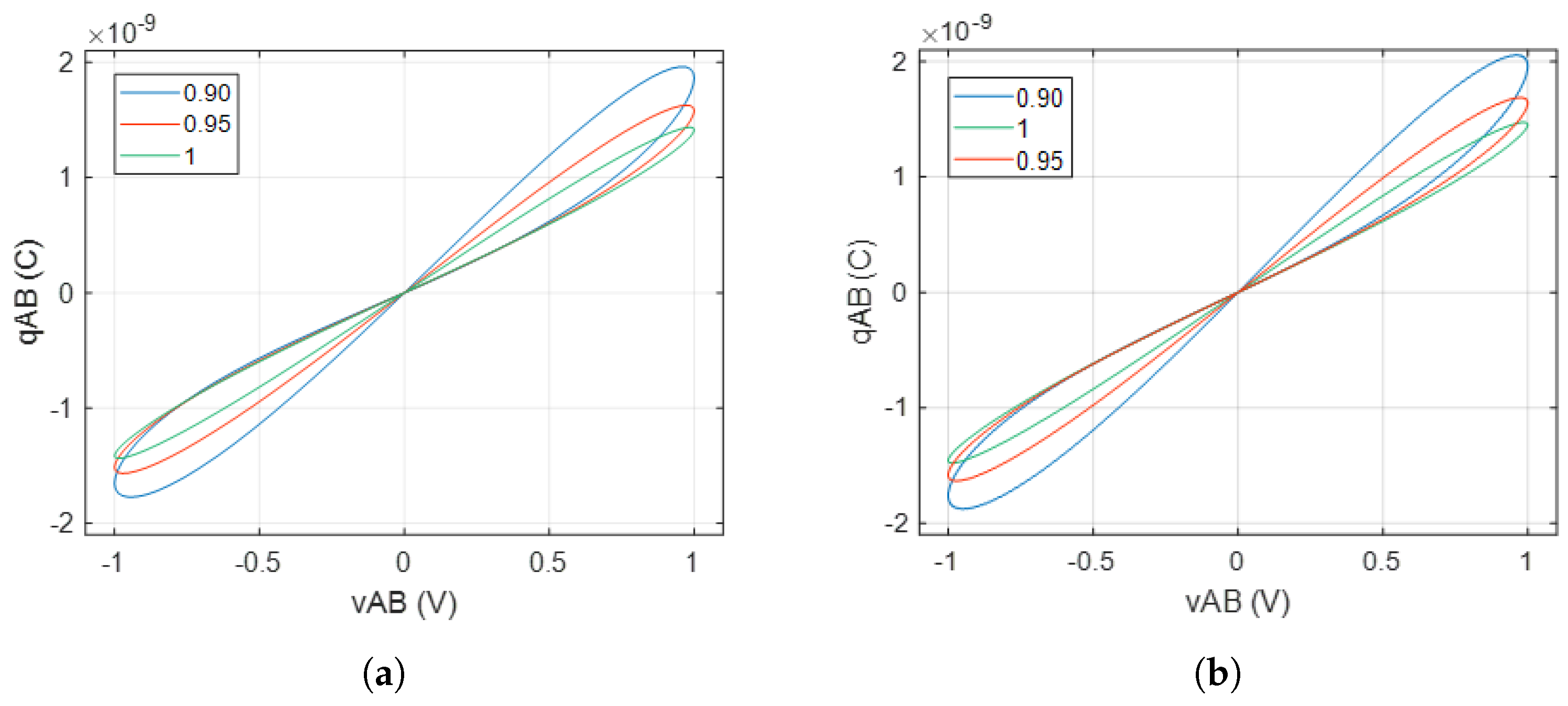
Figure 9a and
Figure 10a present the corresponding results obtained from Matlab, whereas
Figure 9b and
Figure 10b show the results from hardware co-simulation, respectively. Specifically,
Figure 9a,b describe the PHL dynamics of the memcapacitor in the
plane for the aforementioned frequencies at a constant fractional order
= 0.95. In contrast,
Figure 10a,b illustrate the PHL behavior for
= 0.90,
= 0.95 and
= 1 at a constant frequency of 2.5 kHz. The results clearly indicate a significant increase in the lobe area of the hysteresis loop as the fractional-order parameter
decreases, thus demonstrating the impact of the fractional order and the variations in the stimulus frequency on the performance of the emulator.
FOMI Fingerprint
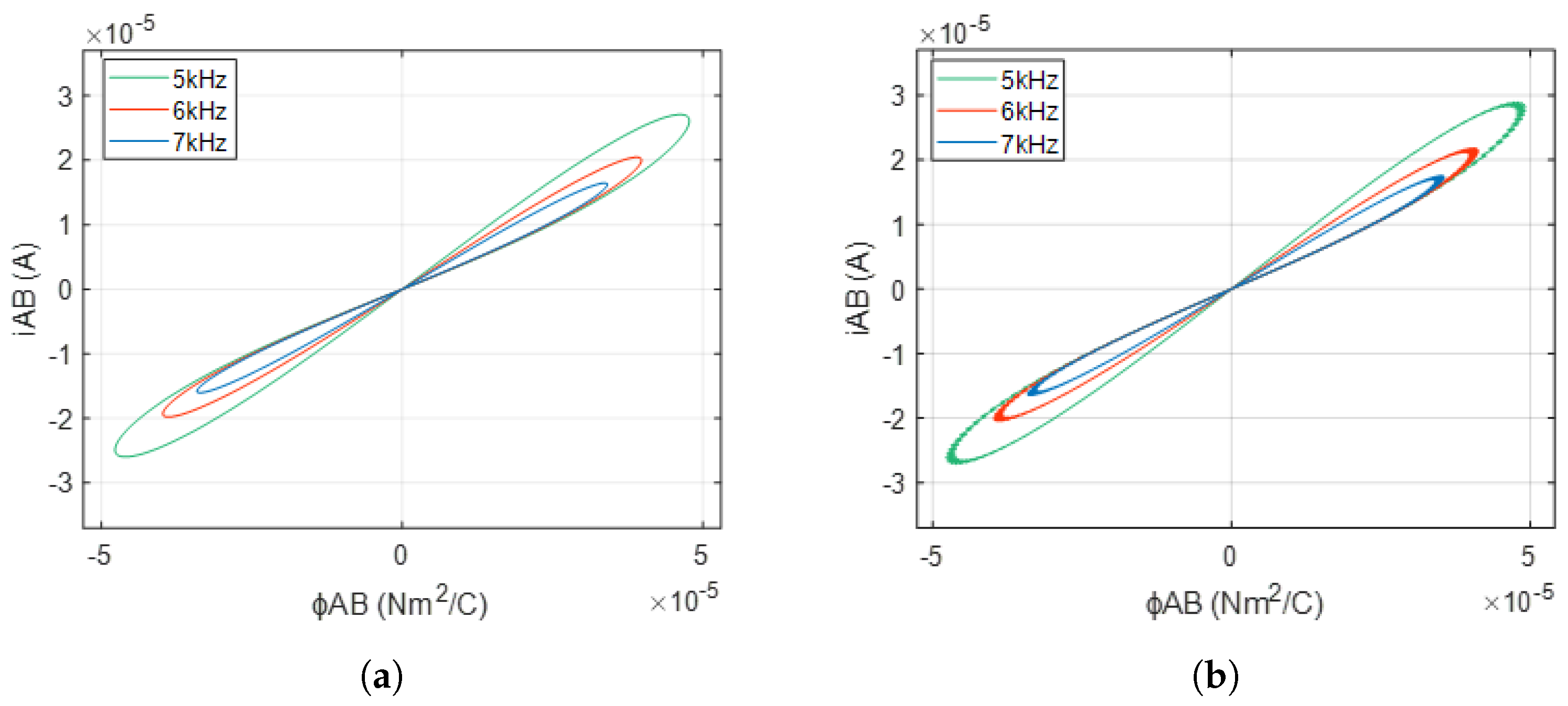
In the case of the FOMI emulator, we evaluated its performance under an input voltage
with a peak amplitude of 1.5 V, across varying excitation frequencies
f = 5 kHz, 6 kHz, and 7 kHz. The system parameters were configured as
= 50 kΩ,
= 10 kΩ,
= 400 mH,
, and
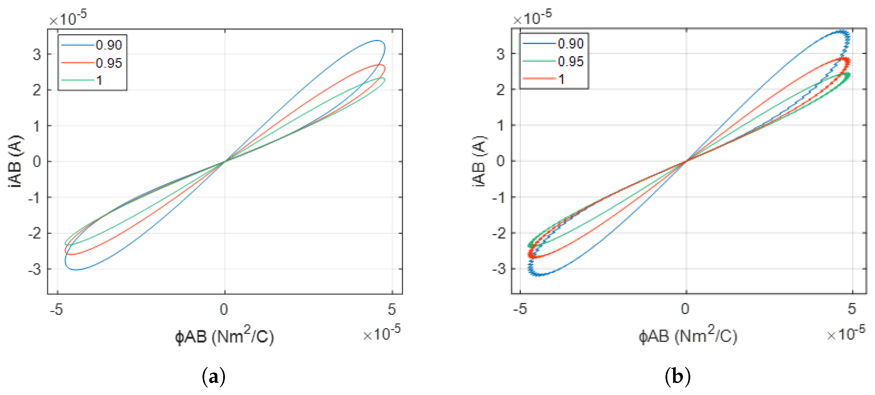
= −8 V. We conducted comparative analyses across fractional-order values of
= 0.90 and
= 0.95, against the integer-order reference
= 1.
Figure 11a,b demonstrate the Matlab simulation and hardware co-simulation results, respectively, for fixed fractional-order parameter and varying frequency, which shows the variation in meminductance in response to the applied voltage, highlighting the degradation of the PHL area as the excitation frequency increases.
Figure 12a,b further illustrate the meminductor’s behavior under constant frequency, while varying the fractional-order parameter. The findings indicate a clear trend: as
increases, the area of the hysteresis loop contracts which signifies diminished meminductance. It is important to mention that while it is obvious that the hardware co-simulation result is consistent with the numerical simulation, the significant discrepancies, particularly the non-smooth behavior around the adaptation threshold of the hysteresis loop, can be primarily attributed to quantization errors that arise from the numerical approximations used in the LUT values.
Resource, Timing and Power Analysis
Table 1 and
Table 2 summarize the hardware description language (HDL) netlist implementation resource utilization for the memelements implemented on the Artix-7 AC701 FPGA evaluation board, using the Vivado synthesis strategy.
Table 1 indicates that the FOMC and FOMI implementations utilize less than
of the available resources, while the FOMR uses approximately
. This difference in resource utilization, despite the similar architectures of these fractional-order designs, can be attributed to the varying number of samples required to complete one stable cycle of the fractional-order integral of the input signal within the LUT. Specifically, the signal frequency influences this sample count: higher frequencies lead to shorter periods and, consequently, a higher number of samples are required within a given timeframe. In our design, we maintain a constant sampling rate of 1 MHz across all configurations of the LUTs, regardless of the frequency used. For instance, with a frequency of 7 kHz, the period
T is approximately 142.86 µs. At a 1 MHz sampling rate, we collect around 143 samples per cycle. In the case of the FOMR, the need for more samples arises from the lower operational frequencies we tested for, compared to the FOMI and FOMC, leading to a greater number of cycles that need to be processed. This results in the higher resource usage in the FOMR design compared to the FOMC and FOMI.
Table 2 provides a detailed overview of the hardware resource utilization for the fractional-order integrals of the driving input signals in their steady-state response for each of the fractional-order memelements. The analysis shows that while the resources required to implement the subsystem account for less than
of the total available FPGA resources across all memelements, the subsystem itself constitutes the larger portion of the overall resource usage.
To evaluate the design’s efficiency in terms of speed and power consumption, we conducted timing and power analyses.
Table 3 presents the timing analysis of the memelements, performed with a timing constraint of a 5
ns (200 MHz) clock period. The negative slack values indicate the extent to which a signal fails to meet its required timing constraint. As shown in
Table 3, the worst negative slack (WNS) across all designs is of positive measure and relatively small. A positive WNS implies that the timing margins are satisfactory, meaning that the designs are not violating their specified timing requirements. Additionally, the total negative slack (TNS) shows zero slack across the designs, affirming that the FPGA implementations meet the required timing specifications.
Table 4 outlines the power consumption of the memelements on the Artix-7 FPGA, revealing an average power usage of about 0.23 W across the three memelements. This low power consumption highlights the efficiency of the memelement implementations, contributing significantly to the overall energy efficiency of the designs. The reduced power usage makes these implementations particularly well suited for a broad range of applications where power efficiency is a critical factor.
