1. Introduction
Dielectric oxides constitute a versatile family of functional ceramics that store and release electrical energy, making them indispensable in capacitors, filters, and sensors. Their performance is primarily governed by the real part of the dielectric permittivity (ε′), which measures the extent of polarization induced by an applied electric field [
1]. Within this family, giant dielectric oxides (GDOs) attract considerable attention because their ε′ values exceed those of conventional dielectrics by several orders of magnitude. Such extraordinary responses are widely ascribed to distinctive microstructural and chemical features [
2,
3], including nanoscale polar microdomains [
4], point and extended defect structures [
5,
6,
7,
8,
9], engineered chemical bonding [
10], grain-boundary polarization, and insulating surface layers [
11,
12]. Together, these factors create internal and interfacial polarization mechanisms that yield the exceptionally high permittivity characteristic of GDOs.
For GDOs, their high ε′ values allow for the miniaturization of components, making them highly valuable in the development of compact electronic devices. The defining feature of GDOs is their enormous dielectric constant. However, they often showed a relatively high loss tangent (tanδ), making them unsuitable for applications in electronic devices [
13,
14,
15]. Additionally, these GDOs frequently exhibit poor temperature stability and frequency dependence in their dielectric properties, which is a crucial problem for various applications. CaCu
3Ti
4O
12 (CCTO) is a GDO that has garnered significant attention due to its giant ε′ [
4,
12,
16,
17]. This property has been observed in a few related oxides as well, which share similar crystal structures and compositions. The mechanism behind this high dielectric constant is often attributed to internal barrier layer capacitance (IBLC) effects [
17], involving the complex microstructure of these materials. Despite their impressive large ε′, CCTO and related oxides often exhibit high tanδ values [
12,
16,
18], which limits their efficiency in practical applications. Another significant limitation is the poor temperature stability of the ε′. This variability hampers their performance in environments where temperature fluctuates, as it affects the reliability and consistency of the device in which they are used.
Titanium dioxide (TiO
2) is a well-known dielectric material with a wide range of applications. Its dielectric properties, however, are moderate in its pure form [
13]. To enhance these properties, scientists have explored co-doping TiO
2 (co-TO) with various ions into the rutile-TiO
2 lattice. The introduction of dopants into the TiO
2 lattice creates defects and alters the electronic structure. This can lead to an increase in the dielectric response (ε′ > 10
4) [
2,
3,
5,
6,
9,
11]. The specific type of dopants used, their concentrations, and the microstructure play crucial roles in determining the extent of the enhancement. For instance, co-dopants like In
3+ and Ta
5+ can create oxygen vacancies and other complex defect states that contribute to higher ε′ [
9]. Various co-TO systems have shown significant improvements in their ε′ values compared to undoped TiO
2. More importantly, this increase in the ε′ is often accompanied by a reduction in the tanδ (<0.05 at ~1 kHz) [
3,
5,
9]. This combination of high ε′ and low tanδ is highly sought after in GDOs for energy storage and electronic applications. Another advantageous property of co-TO is its improved frequency and temperature stability. Unlike some other GDOs, co-TiO
2 can maintain a stable ε′ over a range of frequencies and temperatures, making it suitable for various applications where environmental conditions vary.
While there is extensive research on co-TO, the synthesis processes often involve high-temperature sintering (≥1400 °C) [
3,
5,
6,
9,
11], which is energy-intensive and environmentally taxing. Moreover, the stability of ε′ at different temperatures remains a challenge when sintering at a high temperature. Designing dense co-TO ceramic by sintering at a low temperature is important to save energy of fabrication and obtain excellent temperature stability in a high temperature range. At elevated sintering temperatures, a large concentration of oxygen vacancies is created in TiO
2, releasing free electrons that cannot always be confined in defect complexes [
19]. Upon heating during dielectric measurements, these delocalized electrons contribute to long-range conduction (DC conduction) and high tanδ, while additional interfacial polarization from grain boundaries or electrode interfaces can artificially increase ε′. In contrast, low-temperature sintering suppresses the formation of an excessive concentration of oxygen vacancies (
), stabilizes EPDDs as the dominant mechanism, and thereby improves both dielectric stability and energy efficiency. Basically, dense ceramics can be obtained by using nanoparticles to form a highly dense green body and to increase the driving force from surface free energy [
20], which is enhanced by reducing particle size. The sol–gel method stands as a prominent technique for fabricating ceramic oxide nanoparticles due to its versatility and ability to control particle size and composition [
21]. However, the traditional sol–gel process often involves the use of hazardous chemicals, raising environmental and safety concerns [
20,
22]. The integration of green chemistry principles in nanoparticle synthesis is thus of paramount importance [
23].
An innovative strategy for synthesizing ceramic oxide nanoparticles involves the use of egg white as a green solution in a sol–gel-like process. Egg white-based polymeric solutions provide a sustainable and environmentally friendly alternative, consistent with current trends in green chemistry and eco-conscious materials development [
24,
25]. The proteins in egg white unfold and crosslink during processing, forming a three-dimensional network that effectively traps water and behaves similarly to synthetic polymer gels [
24]. Such characteristics make egg white a promising medium for producing oxide nanoparticles under milder and greener conditions.
In this context, Ta
5+ was chosen as the donor dopant because it has the same ionic radius (64 pm in octahedral coordination) as Nb
5+ but contains an additional electron shell [
26]. First-principles studies indicate that Ta substitution induces stronger lattice distortion around Ti
3+ sites, which enhances electron localization and stabilizes defect states [
9]. When combined with In
3+ as the acceptor dopant, this donor–acceptor pair facilitates the formation of electron-pinned defect dipoles (EPDDs), thereby improving ε′ while reducing tanδ. The choice of In
3+ is particularly advantageous among trivalent acceptors because of its relatively large ionic radius (80 pm) [
26], which differs significantly from that of Ti
4+ (60.5 pm). Bond valence sum (BVS) analyses have shown that substituting Ti
4+ with In
3+ makes In
3+ highly overbonded (apparent valence ~+5.2) [
27], a condition that strongly favors the formation of defect dipole clusters. By contrast, smaller acceptors such as Cu
2+, Ga
3+ or Al
3+ [
28,
29,
30], with ionic radii closer to Ti
4+, induce only weak distortions and are less effective in generating stable defect dipoles. In addition, isovalent dopants such as Hf
4+ or Zr
4+, although chemically compatible with the rutile lattice, do not introduce the charge imbalance required to generate oxygen vacancies or defect dipole clusters. As a result, such substitutions cannot provide the polarization mechanisms necessary for giant dielectric behavior. Unlike single-species doping, such as Nb
5+-doped TiO
2 which yields ε′ > 10
5 but tanδ > 0.5 at 1 kHz [
29,
31], the In
3+ + Ta
5+ pairing provides a more balanced defect chemistry [
9]. It also outperforms several other co-dopant systems (Al
3+ + Nb
5+ [
19,
29], Yb
3+ + Nb
5+ [
32], Y
3+ + Nb
5+ [
33], and Sm
3+ + Ta
5+ [
34]), which generally suffer from tanδ > 0.1 at 1 kHz and strong temperature-dependent dielectric response.
Accordingly, the present work applies the egg-white solution route to synthesize In + Ta co-doped TiO2 (ITTO) nanoparticles, enabling densification at a reduced sintering temperature of 1300 °C. The resulting ceramics were systematically examined for phase purity, microstructure, elemental distribution, and dielectric properties using a comprehensive set of characterization techniques, including field emission scanning electron microscopy (FE-SEM), high-resolution transmission electron microscopy (HR-TEM), X-ray diffraction (XRD), SEM elemental mapping, energy-dispersive spectroscopy (EDS), and X-ray photoelectron spectroscopy (XPS). This study thus combines a sustainable synthesis approach with rational dopant design to achieve ITTO ceramics that exhibit high ε′, low tanδ, and excellent thermal stability of ε′. The purpose of this work is to develop ITTO ceramics through a green egg-white solution route, with emphasis on achieving high dielectric performance at reduced sintering temperatures. This study systematically investigates phase formation, microstructure, and dielectric response, and further employs density functional theory (DFT) calculations to elucidate the role of defect dipoles in governing the giant dielectric behavior.
2. Materials, Equipment and Research Methods
In this experiment, the (In0.5Ta0.5)xTi1−xO2 powders, with x ranging from 0.02 to 0.06, was synthesized using a green solution egg-white method. This composition range lies within the rutile solid-solution regime typically reported for TiO2 co-doping and was expected to yield a balance between densification, ε′, and tanδ. The (In0.5Ta0.5)xTi1−xO2 composition was selected to realize a donor–acceptor co-doping strategy, where In3+ acts as the acceptor and Ta5+ as the donor. The composition window was also designed to balance defect dipole formation with phase stability, since higher substitution levels are known to induce secondary phases or excessive uncontrolled DC conduction. The materials used included C16H28O6Ti (75 wt% in isopropanol), Indium (III) nitrate hydrate (99.9% purity), Tantalum (V) chloride (99.5% purity), ethanol (99.5% purity), acetic acid (99.5% purity), and egg-white. First, an egg-white solution was prepared by mixing 60 mL of egg white with 40 mL of deionized water and stirring continuously with a magnetic stirrer at ~25 °C for 2 h (denoted as solution A). Second, a titanium solution was prepared separately by combining 20 mL of titanium solution, 40 mL of ethanol, and 20 mL of acetic acid with 120 mL of deionized water, while stirring with a magnetic bar at 25 °C for 2 h (denoted as solution B). Third, solution B was gradually blended with 60 mL of solution A, followed by continuous stirring at 25 °C for another 2 h until a smooth gel was formed. Then, the mixture was heated at 120 °C for 5 h to evaporate water and ethanol, eventually yielding a transparent gel. Next, the gel was dried in open air at 350 °C for 1 h at a heating rate of 1 °C/min to remove the organic components. The dried precursor was carefully ground using a mortar and pestle for 30 min. The powder was then calcined at 800 °C for 3 h with heating and cooling rates of 2 °C/min using a Lenton furnace (model UAF 18, Lenton Thermal Design, Hope Valley, UK). After calcination, the powders were again ground with a mortar and pestle to obtain fine powders. Subsequently, the powders were pressed into pellets at a pressure of 180 MPa for 1 min. Finally, the pellets were sintered at 1100–1300 °C for 1 h with a constant heating rate of 5 °C/min using a Lenton furnace (model UAF 18). The bulk density of the sintered ceramics was determined using the Archimedes method with distilled water as the immersion medium. Relative density was determined as the ratio of bulk density to theoretical density, and porosity (%) was calculated using the relation: Porosity (%) = 100 − Relative density (%).
The selected technological parameters, including drying and calcination schedules, pressing pressure, and sintering temperature, were found to exert a strong influence on the structure and properties of the powders and ceramics. Calcination conditions primarily controlled crystallite size and phase purity, while sintering temperature and heating rate determined densification and porosity. These factors directly affected the dielectric response: insufficient densification led to reduced ε′, whereas excessive firing encouraged defect generation and elevated tanδ.
The ITTO powders and sintered ceramics with varying co-doping concentrations were thoroughly characterized using a range of analytical techniques. XRD (PANalytical, Malvern Panalytical, Malvern, UK) was employed to determine the crystal structure, phase composition, and phase purity of both the as-prepared powders and the sintered ceramics. The XRD patterns were recorded over a 2θ range of 20° to 75° with a step increment of 0.02° and a dwell time of 30 s per step. Measurements were performed in continuous (θ–2θ) scanning mode. The diffractometer was operated at 45 kV and 40 mA, using Cu Kα radiation with a wavelength of 0.15406 nm. The microstructure and elemental distribution of the ceramics were examined using FE-SEM equipped with EDS (Helios NanoLab G3 CX, FEI Life Sciences, Hillsboro, OR, USA), operated at an accelerating voltage of 10 kV, along with HR-TEM (Talos F200X, Thermo Fisher Scientific, Waltham, MA, USA) operated at an accelerating voltage of 200 kV. Surface chemical states were investigated using XPS, carried out with a PHI5000 VersaProbe II system (ULVAC PHI, Chigasaki, Japan) at the SUT-NANOTEC-SLRI Joint Research Facility, Synchrotron Light Research Institute (SLRI), Thailand. XPS spectra were deconvoluted using PHI MultiPak software (Version 9.6.0.15), employing Gaussian–Lorentzian mixed function fitting.
To minimize surface effects during electrical measurements, both surfaces of the sintered samples were carefully polished using sandpaper and coated with silver (Ag) paste to form parallel electrodes. The electrode-coated samples were subsequently heated at 600 °C for 0.5 h with a heating rate of 5 °C/min to ensure good electrode adhesion. The polished ceramic samples had thicknesses of 0.77–0.79 mm, and silver paste electrodes with an effective area of 0.196 cm
2 were applied to both surfaces for dielectric measurements. The dielectric properties, including capacitance (C
p) and tanδ, were measured using an impedance analyzer (KEYSIGHT E4990A, Keysight Technologies, Santa Rosa, CA, USA) over a wide frequency range (10
2–10
6 Hz) and a temperature range of 30 to 210 °C using an environmental chamber (DELTA 9023, Cohu Delta Design, Calamba, Philippines), under an applied voltage of V
rms = 0.5 V. To clarify the giant dielectric properties in ITTO, DFT calculations were employed. The detailed computational procedures have been reported in our previous publications [
30]. In particular, the calculations examined the preferred substitutional sites of In
3+ and Ta
5+ ions in the rutile lattice, as well as the energetically favorable configurations of defect complexes involving In
3+-oxygen vacancy and Ta
5+-related defects. The results indicate whether these defects tend to associate spatially, thereby promoting the formation of EPDDs.
3. Results and Discussion
To investigate the phase evolution of the synthesized (In
0.5Ta
0.5)
xTi
1−xO
2 powders, XRD analysis was performed, as presented in
Figure S1 (Supplementary Information, SI). For all powders, the anatase TiO
2 phase (JCPDS No. 21-1272) was dominant, while weak peaks corresponding to a secondary phase, Ti
4O
7 (JCPDS No. 77-1392), were also detected. At
x = 0.06, a gradual transformation from the anatase to the rutile TiO
2 phase (JCPDS No. 21-1276) was observed. This observation is consistent with previous reports, where the rutile phase becomes dominant at calcination temperatures in the range of 700–900 °C [
35]. To strengthen the phase identification, multiple reflections of rutile were indexed against JCPDS No. 21-1276 in both the main text diffractograms and
Figure S1, confirming that the transformation was not based on a single peak. Importantly, no significant peak shift of either anatase or rutile reflections was detected with increasing dopant concentration. A slight broadening of the full width at half maximum (FWHM) of the major diffraction peaks was observed as the dopant concentration increased, particularly at
x = 0.06. This broadening suggests a decrease in the crystallite size [
36], which may be attributed to lattice distortion and inhibited grain growth caused by the incorporation of higher concentrations of In
3+ and Ta
3+ into the TiO
2 lattice. The crystallite sizes were calculated from XRD peak broadening using the Scherrer equation (see Equation (S1) in SI) and were found to be 42.9, 28.2, and 17.4 nm for the (In
0.5Ta
0.5)
xTi
1−xO
2 powders with
x = 0.02, 0.04, and 0.06, respectively. The presence of smaller crystallites, despite the improved phase purity, indicates that the co-doping strategy can suppress excessive grain growth during calcination, potentially improving the sinterability and defect uniformity of the resulting ceramics. Although direct SEM or TEM images of the as-prepared powders prior to calcination are not available, it can be reasonably inferred that these precursors likely fall into the ultrafine regime (<10 nm) [
37], which is characteristic of wet-chemical synthesis methods. Such ultrafine nanoparticles are expected to be significantly smaller than the crystallite sizes obtained after calcination, thereby reflecting the high degree of fineness characteristic of the precursor stage.
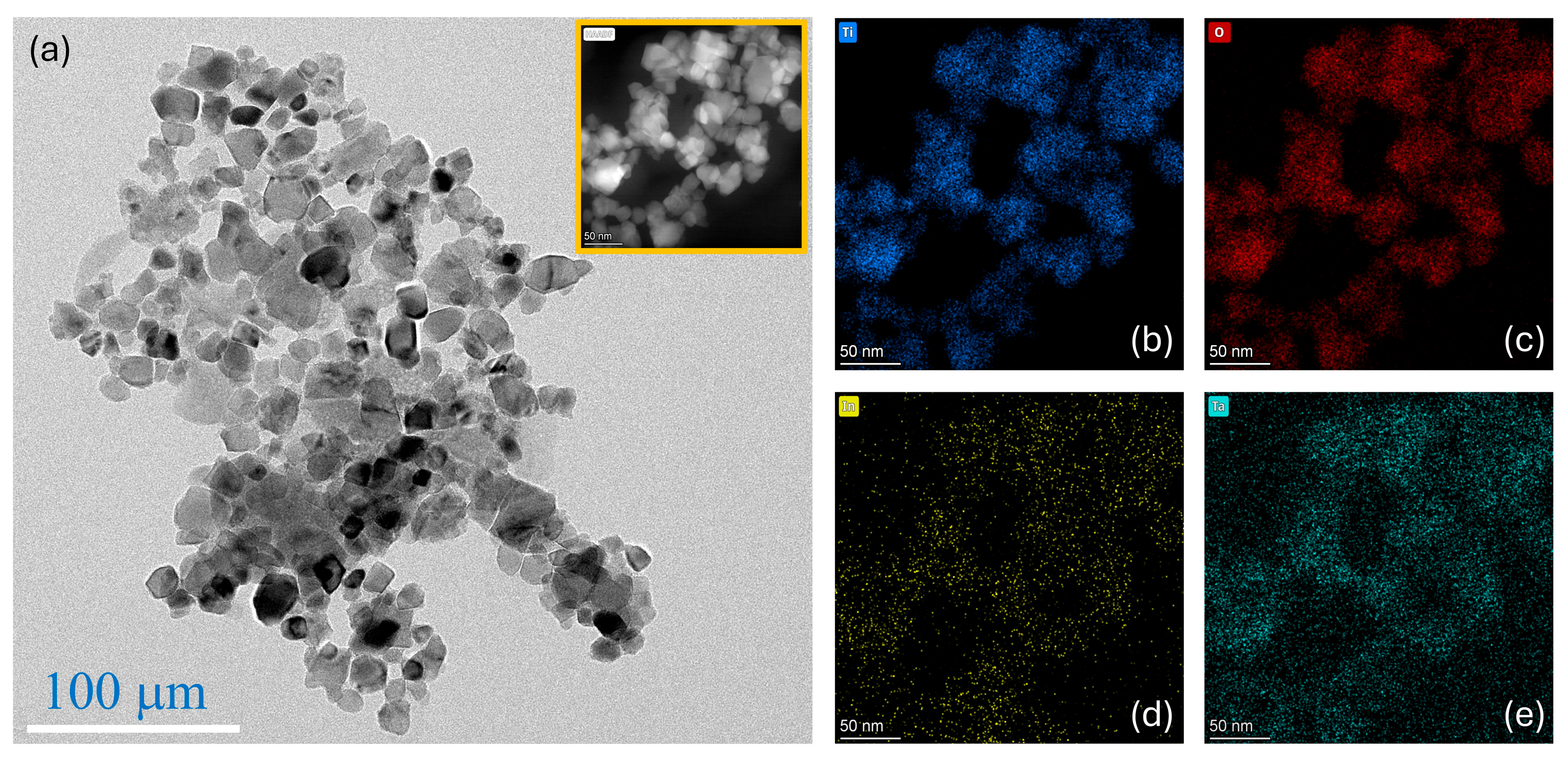
Figure 1 presents the microstructural and compositional characteristics of the synthesized (In
0.5Ta
0.5)
xTi
1−xO
2 powder with
x = 0.06. The HR-TEM image (
Figure 1a) reveals that the particles are aggregated into loosely packed clusters, consisting of uniformly nanosized grains. These grains display predominantly spherical to mildly irregular morphologies, with well-defined boundaries. The average particle size ranges from approximately 20 to 50 nm, which is advantageous for promoting densification during sintering, owing to their high surface energy [
20]. The inset in
Figure 1a shows a high-angle annular dark-field scanning transmission electron microscopy (HAADF-STEM) image, where contrast is enhanced by differences in atomic number. The brighter regions correspond to elements with higher atomic numbers, indicating the presence of In and Ta. This observation confirms the successful incorporation of the doping ions into the TiO
2 matrix.
To evaluate the elemental homogeneity within the nanoparticle aggregates, EDS elemental mapping was conducted, as shown in
Figure 1b–e. The elemental maps of Ti, O, In, and Ta reveal a uniform spatial distribution of all constituent elements throughout the nanopowder. This uniform distribution indicates successful incorporation of the dopants without detectable phase separation or localized elemental enrichment, which is crucial for consistent defect structures and uniform electrical properties within the ceramics. The excellent elemental homogeneity and the nanoscale particle size are expected to significantly promote densification at relatively low sintering temperatures. Such enhancement is primarily attributed to the increased surface energy associated with small particles, providing a strong driving force for densification [
20]. Additionally, the formation of anatase phase during calcination may offer further advantages. Previous studies have indicated that the anatase to rutile phase transformation involves extensive generation of lattice defects, such as oxygen vacancies and interstitials. These defects can enhance atomic diffusion, particularly during the early stages of sintering, thereby facilitating grain contact and promoting effective pore elimination [
20]. Consequently, ceramics exhibiting uniform microstructures and enhanced dielectric properties can be obtained. Supporting data for the nanopowder with
x = 0.04, which demonstrates similar morphological and compositional features but with comparatively larger particle sizes, are provided in
Figure S2 (SI).
The synthesized (In
0.5Ta
0.5)
xTi
1−xO
2 nanoparticles were compacted into green bodies and subsequently sintered at temperatures ranging from 1100 to 1300 °C for 1 h. However, ceramics sintered at 1100 and 1200 °C exhibited porous microstructures, leading to low densification and, consequently, low ε′. Therefore, only the ceramics sintered at 1300 °C, which exhibited improved density, were selected for further investigation.
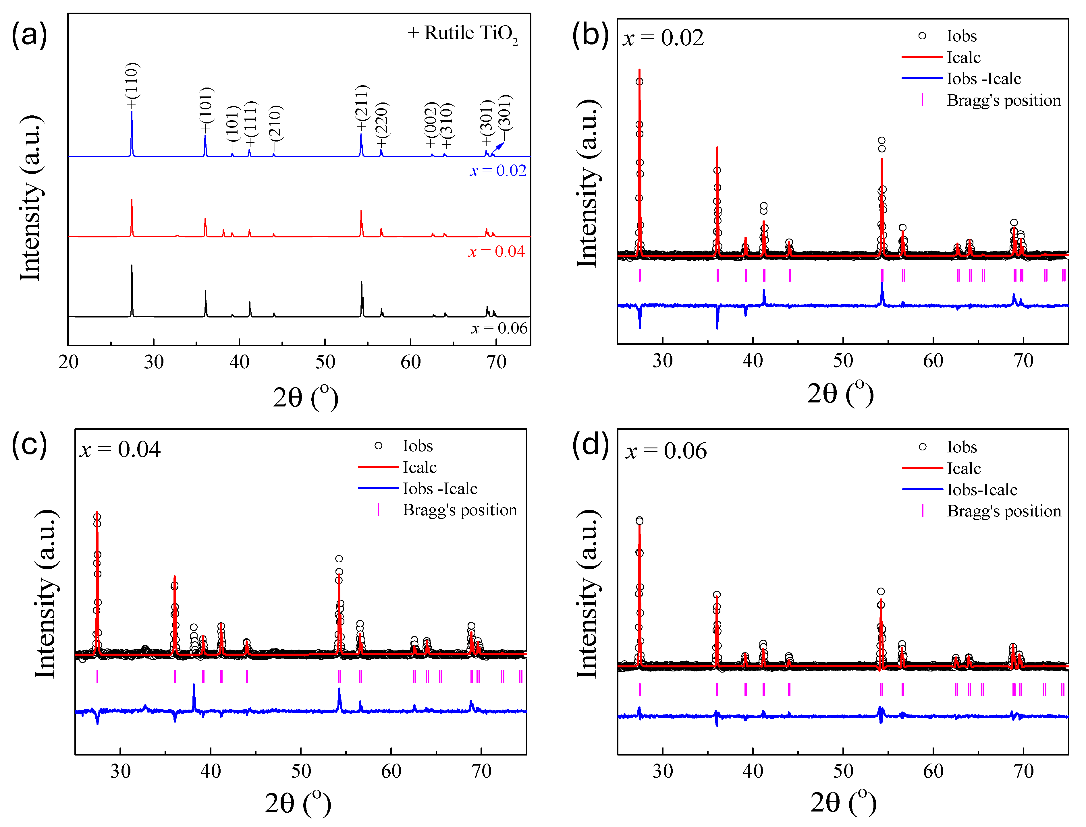
Figure 2a displays the XRD patterns of the sintered (In
0.5Ta
0.5)
xTi
1−xO
2 ceramics with doping levels
x = 0.02, 0.04, and 0.06. All samples exhibit diffraction peaks corresponding exclusively to the rutile TiO
2 phase (JCPDS No. 21-1276) [
5,
11], confirming complete transformation from anatase to rutile during high-temperature sintering. This observation indicates that co-doping with In
3+ and Ta
5+ effectively stabilizes the rutile structure, which is essential for achieving high dielectric performance.
Figure 2b–d present the Rietveld refinement profiles for the sintered ceramics with
x = 0.02, 0.04, and 0.06, respectively. The close agreement between observed and calculated patterns, along with low values of refinement indicators such as
Re,
Rp,
Rwp, and χ
2, confirms the reliability and precision of the structural models used [
38]. The refined lattice parameters, summarized in
Table 1, show a slight but consistent increase with increasing dopant concentration. Specifically, the
a and
b lattice constants increase from 4.597 Å at
x = 0.02 to 4.604 Å at
x = 0.06, while the
c parameter increases from 2.963 Å to 2.971 Å. This gradual lattice expansion is attributed to the substitution of Ti
4+ ions with larger In
3+ and Ta
5+ dopants [
26], resulting in structural distortion and unit cell enlargement. The larger ionic radii of In
3+ and Ta
5+ compared to Ti
4+ contribute directly to this effect. Such lattice modifications are commonly observed in aliovalent-doped rutile systems and are known to influence electrical and dielectric behavior [
27]. Additionally, the increase in Ti–O bond lengths with increasing dopant content further supports the observed lattice expansion. These structural changes confirm the successful incorporation of the dopants into the TiO
2 lattice and suggest the introduction of localized lattice strain, which plays a key role in modifying the polarization behavior and enhancing the dielectric properties of the resulting ceramics. In this study, crystallite sizes were estimated only for the calcined powders using the Scherrer equation. For the sintered ceramics, the diffraction peaks became sharp and narrow, indicating significant grain growth and rendering Williamson-Hall analysis inappropriate. Accordingly, the discussion of sintered samples concentrates on their microstructural features and their effects on dielectric behavior.
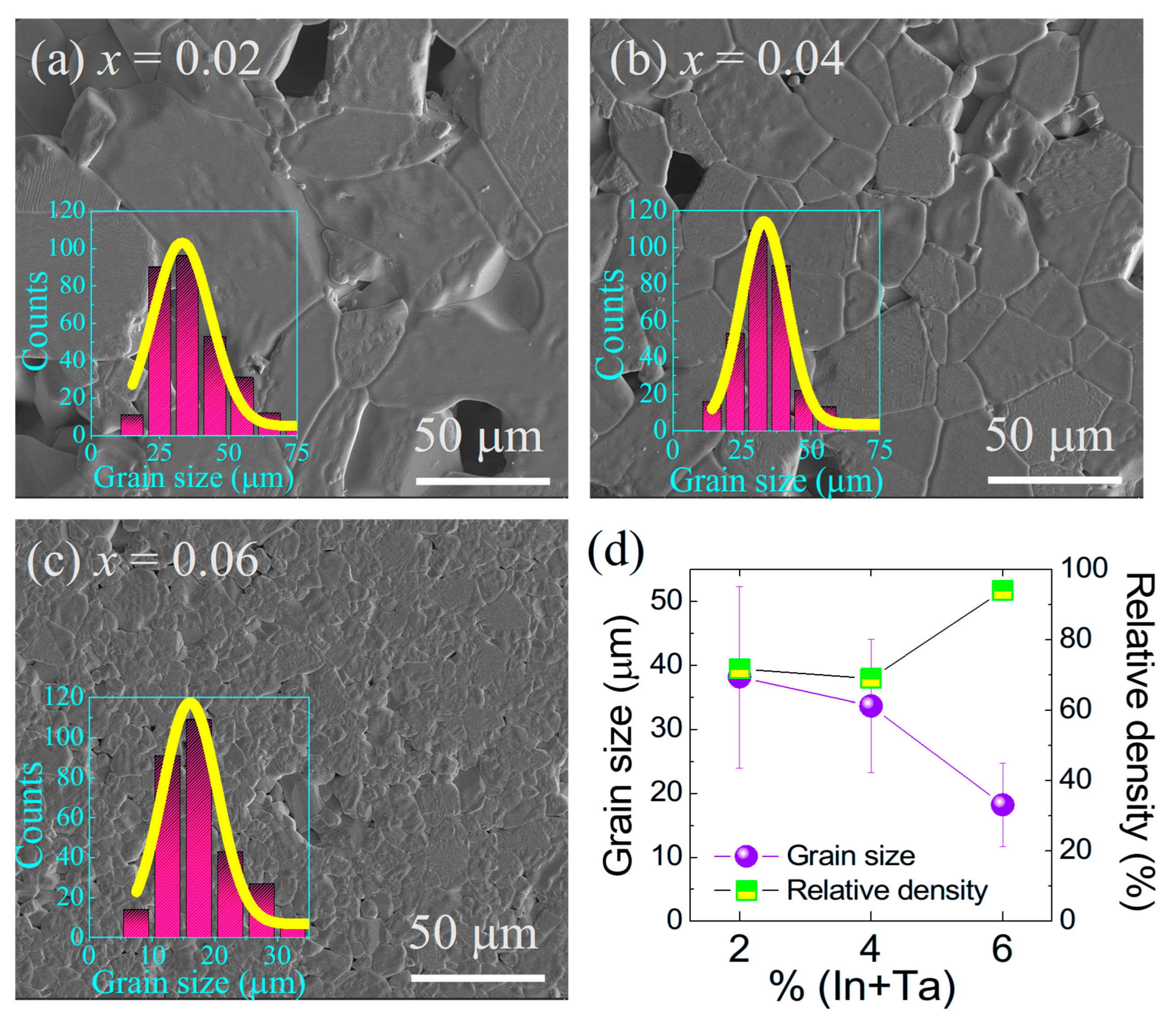
Figure 3a–c presents the SEM micrographs of sintered (In
0.5Ta
0.5)
xTi
1−xO
2 ceramics with dopant concentrations of
x = 0.02, 0.04, and 0.06. At lower doping levels (
x = 0.02 and 0.04), the microstructures exhibit relatively large and irregularly distributed pores, indicating incomplete densification. In contrast, the sample with
x = 0.06 displays a significantly denser and more homogeneous microstructure, with visibly reduced porosity. This trend in porosity and microstructural density is consistent with the crystallite size of the calcined nanopowders. Smaller crystallites possess higher surface free energy, which increases the thermodynamic driving force for sintering. This enhanced driving force promotes densification at a given temperature by accelerating particle rearrangement and grain boundary diffusion [
20]. Therefore, the sample with
x = 0.06, which was prepared from finer nanopowders, achieved greater densification. This relationship between particle size and densification is consistent with previous studies on Ga
3+ + Ta
5+ and Al
3+ + Ta
5+ co-doped TiO
2 ceramics [
30,
39]. The insets in
Figure 3a–c show grain size distributions that are relatively narrow for all compositions, indicating uniform grain growth.
As illustrated in
Figure 3d, the average grain size decreases from 38.16 ± 14.2 μm for
x = 0.02 to 33.64 ± 10.4 μm for
x = 0.04, and further to 18.2 ± 6.6 μm for
x = 0.06. This refinement in grain size with increasing dopant concentration is likely due to the solute drag effect, in which In
3+ and Ta
5+ ions introduce localized lattice strain and reduce grain boundary mobility [
9,
40], thus suppressing grain coarsening during sintering [
20,
41]. The relative density measurements shown in
Figure 3d further support this microstructural evolution. The ceramics with
x = 0.02 and 0.04 exhibit relative densities of ~71% and ~70%, respectively, whereas the sample with
x = 0.06 achieves a significantly higher density of ~94%. The improved densification at the highest doping level can be attributed to the reduced particle size of the initial powders, which facilitates tighter packing in the green body and enhances sintering kinetics [
20,
42]. These results demonstrate that increasing the total dopant concentration not only promotes densification but also refines grain size. The improved microstructural uniformity observed in the
x = 0.06 ceramic is expected to have a positive impact on the dielectric performance, as it minimizes porosity and enhances grain boundary integrity. The chemical interaction during sintering occurs primarily through the incorporation of In
3+ and Ta
5+ into the TiO
2 lattice as a solid solution rather than through the formation of separate phases. XRD patterns of the calcined powders reveal anatase TiO
2 as the dominant phase with only weak reflections assignable to Ti
4O
7, while no segregated In- or Ta-rich oxides are detected within the detection limit. HR-TEM and EDS mapping further indicate a homogeneous nanoscale distribution of the dopants, suggesting that In
3+ and Ta
5+ are incorporated into the TiO
2 lattice. After sintering, all compositions exhibit single-phase rutile TiO
2 confirmed by Rietveld refinement, supporting the solid-solution formation of In/Ta in the rutile lattice. This dopant incorporation alters the defect chemistry, enhancing diffusion and promoting densification while simultaneously retarding abnormal grain growth through a solute-drag effect [
20]. As a result, the optimized composition (
x = 0.06, 1300 °C) attains high relative density with minimal porosity and a uniform grain structure, which are directly correlated with the improved dielectric response observed in the present study. Although systematic mechanical testing was not undertaken in this work, the dense and uniform microstructure of the optimized sample strongly suggests favorable mechanical robustness, which will be quantitatively evaluated in future studies.
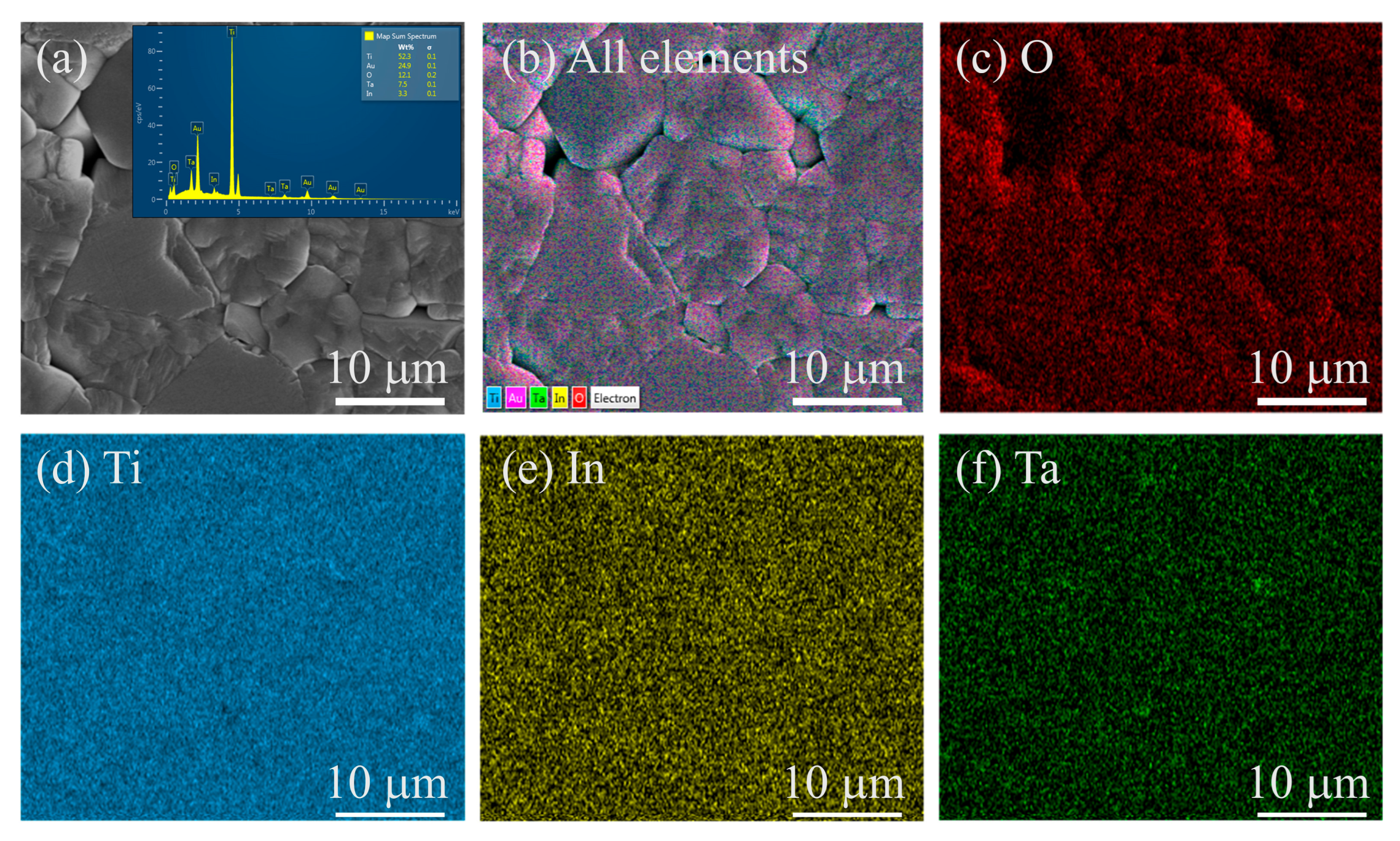
Figure 4 illustrates the elemental distribution in the (In
0.5Ta
0.5)
xTi
1−xO
2 ceramic with
x = 0.06. The SEM image in
Figure 4a shows a representative microstructure with well-developed grains and minimal porosity. The corresponding EDS spectrum confirms the presence of Ti, O, In, and Ta, with no detectable secondary elements or contamination. Elemental mapping images (
Figure 4b–f) reveal that all elements are uniformly dispersed throughout the examined area. The overlay map in
Figure 4b demonstrates a consistent distribution pattern across the grain structure, while individual maps of O, Ti, In, and Ta confirm the absence of elemental segregation or localized clustering. This homogeneous distribution suggests effective incorporation of the dopants into the TiO
2 lattice during synthesis and sintering.
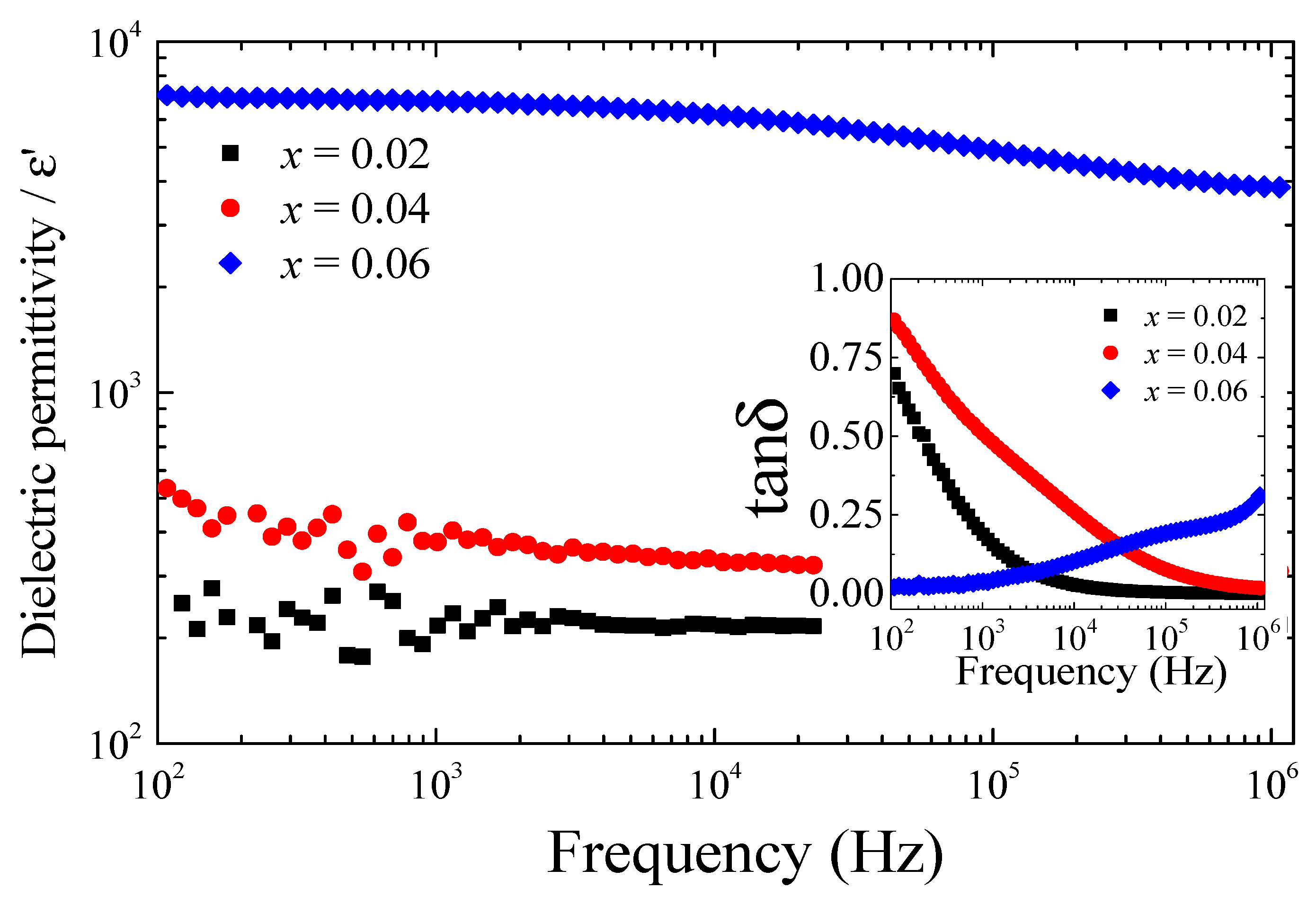
Figure 5 displays the ε′ and tanδ (inset) as a function of frequency at 30 °C for (In
0.5Ta
0.5)
xTi
1−xO
2 ceramics with
x = 0.02, 0.04, and 0.06. The ceramics with lower doping concentrations (
x = 0.02 and 0.04) did not exhibit a giant dielectric response, as their ε′ values remained below 10
3 across the entire frequency range. Specifically, their dielectric permittivity at 1 kHz was ~217 and ~375, respectively. Moreover, both samples showed high tanδ values, particularly at low frequencies, indicating significant dielectric loss and limited capacitive behavior. In contrast, the ceramic with
x = 0.06 demonstrated a pronounced giant dielectric response, with a ε′ value of ~6780 at 1 kHz. Notably, the corresponding tanδ was remarkably low at 0.038, which is comparable to values typically observed in co-TO ceramics sintered at much higher temperatures [
3,
5,
27,
30,
39]. The ability to achieve such a low tanδ at a reduced sintering temperature of 1300 °C highlights the effectiveness of the nanoparticle-assisted sintering approach in this study. The low ε′ values and high tanδ observed in the
x = 0.02 and 0.04 ceramics are closely related to their microstructural characteristics, particularly their relatively low relative densities. The presence of a significant number of air-filled pores, which have inherently low permittivity (ε′~1), reduces the effective dielectric response of the ceramic matrix. This correlation between porosity and reduced ε′ is consistent with the microstructural observations described earlier. Furthermore, the ε′ value of the
x = 0.06 ceramic showed only a slight dependence on frequency in the range of 40 to 10
4 Hz, indicating dielectric stability across this bandwidth. In contrast, the large increase in loss tangent at low frequencies in the
x = 0.02 and 0.04 samples is likely attributed to DC conduction effects [
43], which typically dominate in the low-frequency regime near the electrode interface [
44].
In the investigated composition range (
x = 0.02–0.06) and sintering temperatures of 1100–1300 °C, the sample with
x = 0.06 sintered at 1300 °C for 1 h exhibited the most favorable balance of high ε′, low tanδ, and high relative density. At 1200 °C none of the compositions showed a significant increase in ε′, which we attribute to incomplete densification and limited incorporation of the donor species at this lower firing temperature. Under low-temperature sintering, donor solubility and defect formation are strongly concentration-dependent; for
x < 0.06 the donor level is insufficient to generate a robust population of defect complexes with In
3+ [
5,
45], leading to weak dielectric response. While sintering above 1300 °C or using higher dopant levels might further alter the dielectric behavior [
46], such conditions are generally associated with an increased oxygen-vacancy concentration and increased free-electron conduction, which elevate tanδ and destabilize the temperature dependence. The focus of this study was to develop a low-temperature sintering route using egg-white-derived nanoparticles, both to reduce processing energy and to improve dielectric stability. Accordingly,
x = 0.06 at 1300 °C is identified as an optimum condition within the investigated range, rather than a global optimum. These findings highlight that chemical composition plays a decisive role in governing the dielectric performance of ITTO ceramics. Too little substitution (
x < 0.06) fails to generate a sufficient density of defect dipoles, while excessive substitution (
x > 0.06) or higher sintering temperatures are prone to increase oxygen vacancies and conduction losses. Thus, the In
3+/Ta
5+ co-doping level and sintering temperature must be carefully balanced, with
x = 0.06 at 1300 °C providing the most favorable condition within the present study window.
Figure 6 presents the dielectric properties of the sintered (In
0.5Ta
0.5)
xTi
1−xO
2 ceramics at ~1 kHz as a function of temperature in the range from 30 to 210 °C. As shown in
Figure 6a, all sintered ceramics demonstrate only slight variations in ε′ across the measured temperature range, indicating a general stability in dielectric response with temperature. However, significant differences in the absolute values of ε′ are clearly observed among these compositions. The ceramics with lower doping concentrations (
x = 0.02 and 0.04) exhibit relatively low ε′ values, reflecting values of less than 10
3. In contrast, the ceramic with the highest doping concentration (
x = 0.06) displays a notably high ε′, which remains stable across the entire temperature range. Such outstanding temperature stability of the ε′ value is particularly desirable yet rarely observed in many GDOs such as CaCu
3Ti
4O
12 [
12,
16], Dy
2NiMnO
6 [
47], Ba(Fe
1/2Ta
1/2)O
3 [
48], and NiO [
43], which typically suffer from substantial temperature-dependent variations in ε′, accompanied by significantly high tanδ.
Further emphasizing its exceptional performance, the ceramic with
x = 0.06 also maintains very tanδ throughout the measured temperature interval (inset of
Figure 6a). The tanδ values remain consistently low over a broad temperature range, a key factor enhancing the suitability of this ceramic for practical capacitor applications. Low tanδ is critical, as it reduces energy dissipation during operation, thus improving device efficiency [
1,
13,
15]. To quantify dielectric performance under varying thermal conditions, the temperature coefficient of dielectric permittivity (Δε′(%)) at ~1 kHz was calculated, as illustrated in
Figure 6b. According to the Electronic Industries Alliance (EIA) standard [
14], capacitor materials classified as X–R must exhibit Δε′ values within ±15% across the specified operational temperature range. Notably, the ceramic with
x = 0.06 exhibits an exceptionally low Δε′ of less than ±4%, even at elevated temperatures up to 200 °C. Such stability is highly advantageous and surpasses the typical performance of most GDOs, which generally display pronounced temperature-dependent behavior above 100 °C [
12]. The ceramic with
x = 0.06 demonstrates remarkable dielectric performance, combining high ε′, consistently low tanδ, and outstanding temperature stability. As summarized in
Table 2, the ITTO ceramics developed in this work exhibit a desirable combination of high ε′, low tanδ, and stability up to 200 °C, while being processed at a reduced sintering temperature of 1300 °C. Although the absolute ε′ values are lower than some other reported GDOs, the present ceramics achieve optimized dielectric properties because those higher-ε′ systems typically suffer from excessive tanδ or severe temperature dependence, which limit their practical applicability. This balance of properties highlights the main advantage of the present ITTO ceramic over other GDOs: it combines high ε′ with suppressed tanδ and reliable thermal stability, while being fabricated by a green, low-temperature route. These features make it more promising for practical capacitor applications than systems that show extreme ε′ but poor efficiency or limited operational stability.
Beyond EPDD, an interfacial Maxwell-Wagner (MW) response is likely to contribute in doped TiO
2 ceramics [
49,
50]. Electrical contrast between semiconducting grains and resistive grain boundaries can produce an IBLC effect that increases ε′ while keeping tanδ low. For
x = 0.06, ε′~6780 at 1 kHz and tanδ ~0.038 with only weak dispersion up to 10
4 Hz, together with refined grains and high relative density, are consistent with grain- and grain-boundary-controlled interfacial polarization acting alongside EPDD. Taken together, the present microstructural and dielectric trends, together with prior reports on co-doped rutile, support a cooperative picture in which EPDD is the primary mechanism and MW/IBLC is complementary.
The low ε′ observed for the x = 0.02 and 0.04 samples can be partly attributed to their higher porosity and incomplete densification, since pores act as regions with a ε′ value close to unity and thus reduce the effective ε′ of the ceramic matrix. Porosity further diminishes grain-grain contacts, weakening interfacial polarization contributions such as the IBLC effect, even though EPDD remains the dominant mechanism in this system. In addition, pores function as stress concentrators in brittle ceramics, serving as initiation sites for crack propagation and thereby lowering fracture strength and reliability under mechanical or thermal stress. Consequently, if porosity persists, the material behaves as a composite of dense ceramic and air-filled voids, which contributes to a reduced dielectric constant, increased fragility, and potential degradation in long-term operational stability due to moisture uptake.
Table 2.
Summary of dielectric properties (at 1 kHz and 25 °C) and sintering conditions of (In0.5Ta0.5)xTi1−xO2 ceramic with x = 0.06 obtained via the egg-white solution method, benchmarked against other co-TO ceramics prepared using alternative synthesis methods.
Table 2.
Summary of dielectric properties (at 1 kHz and 25 °C) and sintering conditions of (In0.5Ta0.5)xTi1−xO2 ceramic with x = 0.06 obtained via the egg-white solution method, benchmarked against other co-TO ceramics prepared using alternative synthesis methods.
| Co-Dopants | ε′ | tanδ | Δε′ (%) at 200 °C | Sintering Conditions | Preparation Method | Ref. |
|---|
| In3+/Ta5+ | 6.8 × 10³ | 0.038 | 3.9% | 1300 °C/1 h | egg-white solution | This work |
| Sm3+/Ta5+ | ~2.3 × 10⁴ | ~0.1 | – | 1500 °C/10 h | SSR | [34] |
| Al3+/Ta5+ | ~1.1 × 10⁴ | 0.012 | >15% | 1500 °C/5 h | SSR | [39] |
| In3+/Nb5+ | 5.1 × 10⁴ | 0.03 | >15% | 1400 °C/10 h | SSR | [46] |
| In3+/Nb5+ | ~1.9 × 10⁴ | 0.08 | >15% | 1500 °C/1 h | Sol–gel | [11] |
| Ga3+/Ta5+ | 5.6 × 10³ | 0.009 | >15% | 1500 °C/5 h | SSR | [30] |
| Zn2+/Ta5+ | ~1.3 × 10⁴ | ~0.27 | >15% | 1050 °C/0.4 h | Flash sintering | [51] |
| Al3+/Nb5+ | ~3.0 × 10⁴ | ~0.1 | >15% | 1500 °C/20 h | SSR | [29] |
| Yb3+/Nb5+ | ~1.0 × 10⁴ | ~0.2 | >15% | 1420 °C/10 h | SSR | [32] |
| Y3+/Nb5+ | ~2.0 × 10⁴ | ~0.2 | >15% | 1500 °C/2 h | Chemical combustion | [33] |
| Mg2+/Nb5+ | ~8.0 × 10⁴ | ~1.0 | >15% | 1100 °C/0.3 h | Flash sintering | [52] |
| Ca2+/Nb5+ | ~2.0 × 10⁵ | ~2.0 | >15% | 1100 °C/0.3 h | Flash sintering | [52] |
| Sr2+/Nb5+ | ~3.0 × 10⁵ | ~2.5 | >15% | 1100 °C/0.3 h | Flash sintering | [52] |
| Ba2+/Nb5+ | ~5.0 × 10⁵ | ~3.0 | >15% | 1100 °C/0.3 h | Flash sintering | [52] |
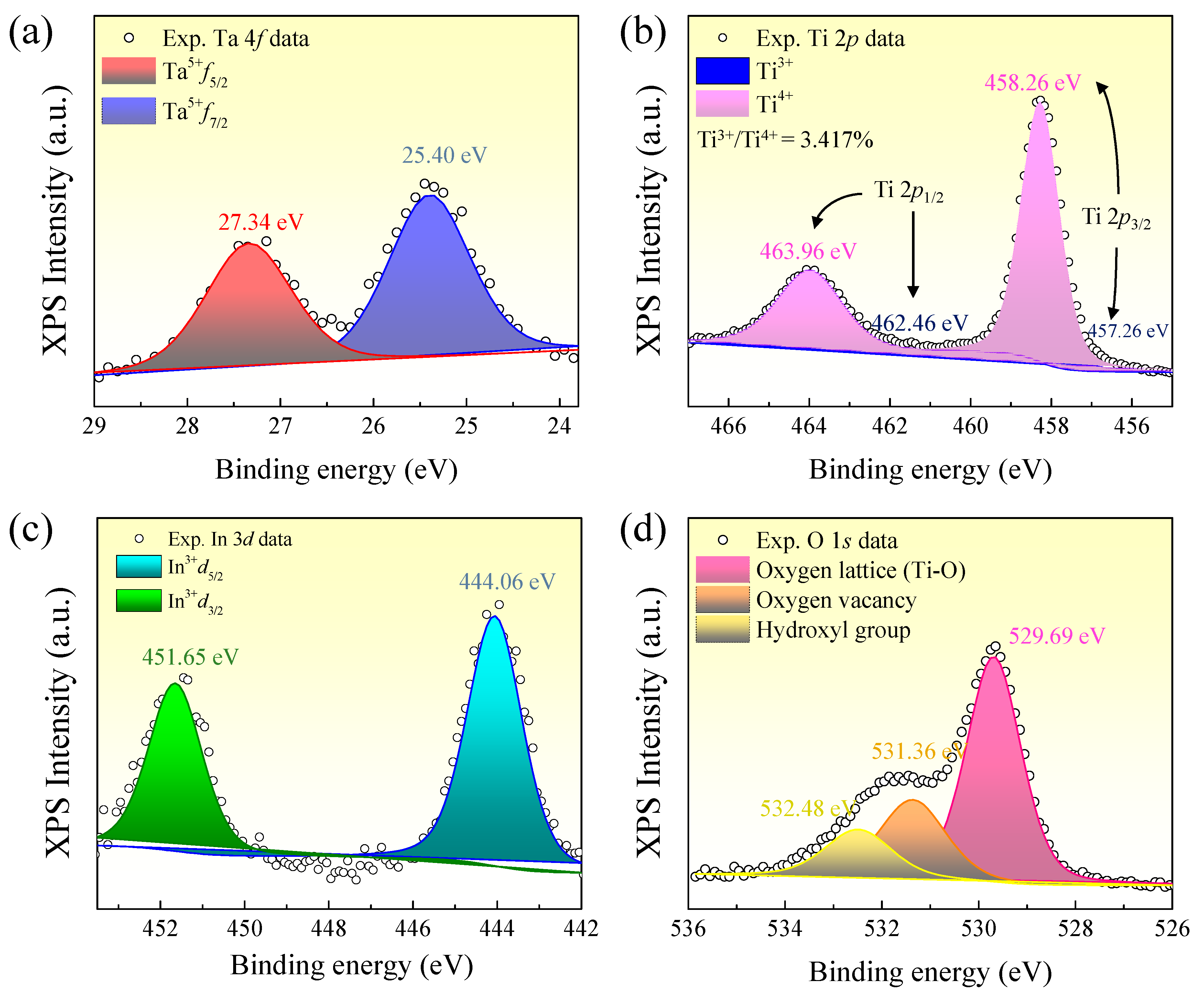
Figure 7 displays the high-resolution XPS spectra of the (In
0.5Ta
0.5)
xTi
1−xO
2 ceramic with
x = 0.06 for the regions of Ta 4
f, Ti 2
p, In 3
d, and O 1
s. These spectra provide important insights into the oxidation states of the constituent elements and reveal the presence of point defects that are closely linked to the dielectric response. As shown in
Figure 7a, the Ta 4
f spectrum exhibits two distinct peaks at binding energies (BEs) of 25.4 eV and 27.34 eV, indicating to Ta 4
f7/2 and Ta 4
f5/2, respectively [
9,
30], which are characteristic of Ta
5+. This confirms that Ta
5+ ions were successfully incorporated into the TiO
2 lattice without evidence of secondary phases or partial reduction. As a donor dopant, Ta
5+ introduces excess electrons, which may become localized on neighboring Ti sites and reduce Ti
4+ to Ti
3+. The XPS spectrum of Ti 2
p (
Figure 7b) was divided into four peaks. The Ti 2
p3/2 peaks were identified at BEs of 457.26 eV and 458.26 eV, corresponding to Ti
3+ and Ti
4+ [
5,
6,
9,
30], respectively. The associated Ti 2
p1/2 peaks appeared at the BEs of 462.46 eV and 463.96 eV. The ratio of Ti
3+:Ti
4+ was calculated to be ~3.3%:96.7%. This value is close to the theoretical prediction for the (In
0.5Ta
0.5)
0.06Ti
0.94O
2 composition. This reduction of Ti
4+ is attributed to the electron donation from Ta
5+, following the reactions [
39]:
The presence of Ti3+ provides compelling evidence for the formation of localized electron-rich local structures, which are essential for the development of EPDDs.
As shown in
Figure 7c, the XPS spectrum of In 3
d exhibits two distinct peaks at BEs of 444.06 eV and 451.65 eV, corresponding to the In 3
d5/2 and In 3
d3/2 components, respectively [
5]. These values are consistent with trivalent indium (In
3+), confirming that the dopant ions were successfully substituted into the rutile TiO
2 lattice structure in their expected oxidation state.
Figure 7d displays the XPS spectrum of O 1
s, which was divided into three peaks located at the BEs of 529.69 eV, 531.36 eV, and 532.48 eV. The strongest peak at BE of 529.69 eV is attributed to lattice oxygen bonded in the Ti–O [
5,
6,
9,
30]. The second peak at BE of 531.36 eV is assigned as oxygen vacancies (
) or oxygen atoms in non-stoichiometric environments linked to lattice defects [
30]. The next at 532.48 eV is usually assigned to surface hydroxyl groups or adsorbed water [
30]. The appearance of the
-related signal confirms the presence of oxygen-deficient regions, which are generally introduced through the substitution of Ti
4+ by In
3+.
This substitution results in a charge imbalance, which is compensated by the formation of
, following the defect reaction [
5]:
The generation of
, together with the presence of Ti
3+ centers, creates localized defect clusters, which play a significant role in enabling the giant dielectric response. These defects support the creation of point defect clusters, which contribute to dielectric polarization by introducing localized charge centers within the rutile structure [
5,
9].
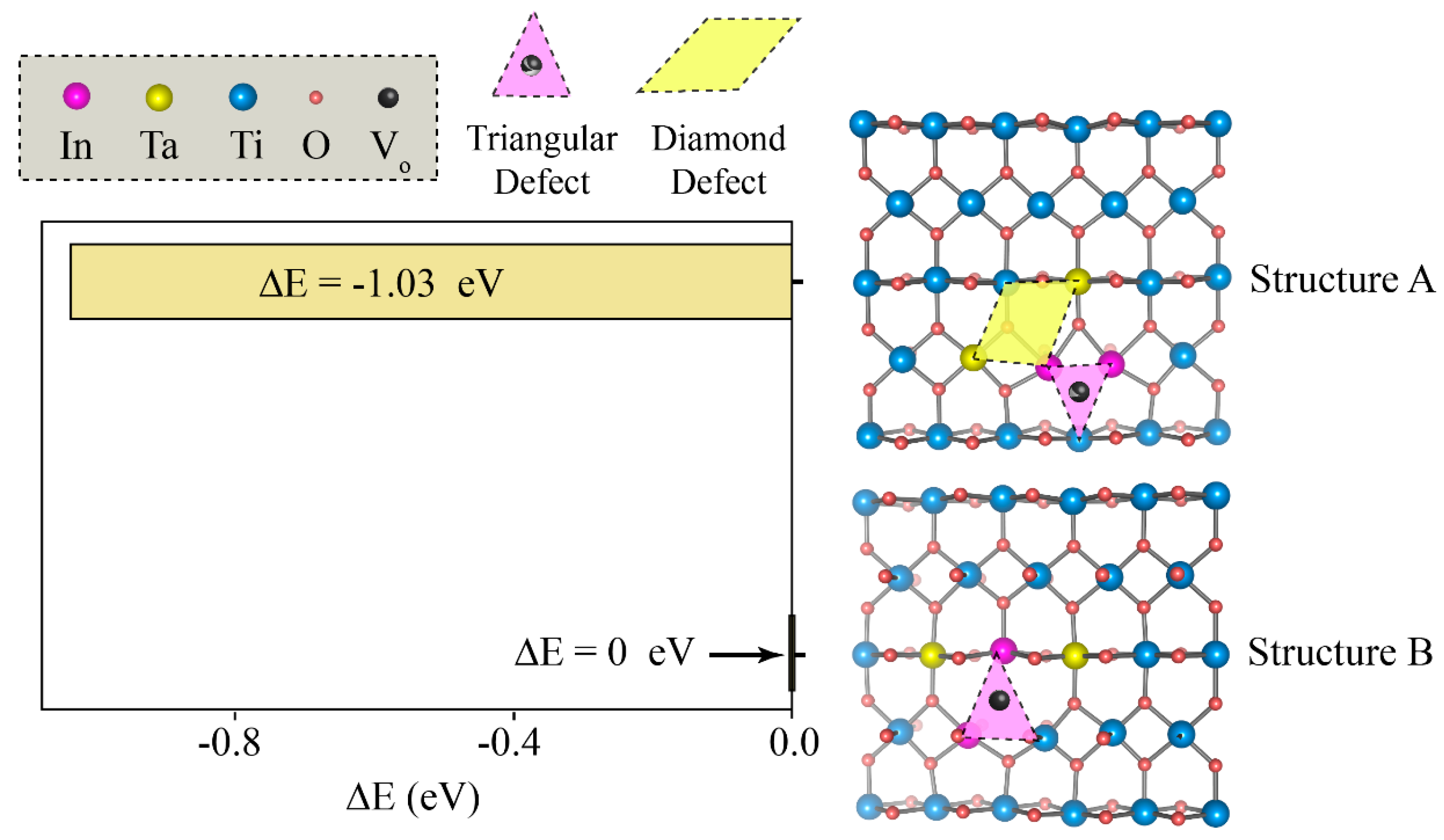
To investigate whether the point defects identified by XPS assemble into stable electron-trapping clusters, we performed DFT calculations to compare the stability of two defect configurations: Structure A and Structure B. Structure A consists of a triangle-diamond cluster linking an
unit with a Ta-centered diamond-like configuration. In contrast, Structure B features a triangle-line arrangement with Ta
5+ ions positioned on either side of an In
3+ apex along the [001] direction, which produces an additional reduced Ti
3+ ion in a neighboring octahedron. To determine their stability, we calculated the total energy difference (ΔE) using Structure B as the reference (ΔE = 0). Since the configuration with the lowest total energy is the most stable, the structure with the most negative ΔE is thermodynamically favored. As shown in
Figure 8, Structure A has a ΔE of −1.03 eV, while Structure B, by definition, is 0.00 eV. Consequently, Structure A is more stable than Structure B. This result indicates a thermodynamic preference for the compact association of In
3+,
, and Ta-related defects, as realized in Structure A. In both structures, the electrons donated by Ta
5+ remain localized on adjacent Ti sites, as confirmed by the calculated spin densities, thus providing the essential requirement for the EPDD mechanism [
5]. These theoretical insights complement the experimental XPS analysis, which confirmed the successful incorporation of In
3+ and Ta
5+ into the TiO
2 lattice and revealed the presence of intrinsic point defects such as Ti
3+ species and oxygen vacancies. Together, the XPS signatures and the DFT energetics provide a coherent picture in which EPDDs emerge as the dominant source of dielectric polarization in these ceramics. The defect clusters are most likely to adopt triangle-diamond or triangle-line geometries, where Ta
5+-donated electrons are pinned on Ti sites adjacent to In
3+ and nearby
, thereby enhancing dielectric polarization while suppressing long-range conduction.
The egg-white solution method further enabled the synthesis of chemically homogeneous nanoparticles, which facilitated complete densification at 1300 °C and yielded a fine, pore-free rutile microstructure with uniformly distributed dopants. This optimized microstructural state suppressed electronic conduction, reinforced the contribution of localized defect dipoles, and ultimately led to the simultaneous realization of high ε′, low tanδ, and excellent thermal stability in ITTO ceramics.
