Article

Unveiling the Potential of Novel Ternary Chalcogenide SrHfSe3 for Eco-Friendly, Self-Powered, Near-Infrared Photodetectors: A SCAPS-1D Simulation Study

School of Engineering and Information Technology, University of New South Wales at Canberra, Northcott Drive, Canberra, ACT 2610, Australia
*
Author to whom correspondence should be addressed.
Sci 2025, 7(3), 113; https://doi.org/10.3390/sci7030113
Submission received: 30 June 2025 / Revised: 29 July 2025 / Accepted: 3 August 2025 / Published: 6 August 2025

Abstract

Ternary chalcogenide-based sulfide materials with distorted morphologies such as BaZrS3, CaZrS3, and SrZrS3, have recently gained much attention in optoelectronics and photovoltaics due to their high structural and thermal stability and compatibility with low-cost, earth-abundant synthesis routes. However, their relatively large bandgaps often limit their suitability for near-infrared (NIR) photodetectors. Here, we conducted a comprehensive investigation of SrHfSe3, a ternary chalcogenide with an orthorhombic crystal structure and distinctive needle-like morphology, as a promising candidate for NIR photodetection. SrHfSe3 exhibits a direct bandgap of 1.02 eV, placing it well within the NIR range. Its robust structure, high temperature stability, phase stability and natural abundance make it a compelling material for next-generation, self-powered NIR photodetectors. An in-depth analysis of the SrHfSe3-based photodetector was performed using SCAPS-1D simulations, focusing on key performance metrics such as J–V behavior, photoresponsivity, and specific detectivity. Device optimization was achieved by thoroughly altering each layer thickness, doping concentrations, and defect densities. Additionally, the influence of interface defects, absorber bandgap, and operating temperature was assessed to enhance the photoresponse. Under optimal conditions, the device achieved a short-circuit current density (Jsc) of 45.88 mA/cm2, an open-circuit voltage (Voc) of 0.7152 V, a peak photoresponsivity of 0.85 AW−1, and a detectivity of 2.26 × 10¹⁴ Jones at 1100 nm. A broad spectral response spanning 700–1200 nm confirms its efficacy in the NIR region. These results position SrHfSe3 as a strong contender for future NIR photodetectors and provide a foundation for experimental validation in advanced optoelectronic applications.

1. Introduction

Photodetectors are optoelectronic gadgets that convert optical signals into their equivalent electrical signals [1]. The process begins when the absorber material interacts with incoming photons, leading to the generation of electron–hole pairs. These charge carriers are then driven by an internal electric field, resulting in the production of a photocurrent or electrical signal [2]. They are currently becoming indispensable devices in our daily life due to their various applications from optical communication to environmental sensing, missile warning, aviation, target detection, biomedical imaging, and security [3,4,5,6].
To evaluate the photodetector performance, various performance metrics are required to fully determine the device’s capability. The detector responsivity quantifies how the device can convert the input light intensity into an electrical signal. It is primarily governed by the material’s charge transport properties, carrier mobility, and optical absorption [7]. The dark current, which is the response of the photodetector while there is no illumination, represents the saturation carrier flow. Elevated dark current levels may obscure weak photocurrent signals and degrade the signal-to-noise ratio. The detectivity, however, is the measure of the photodetector’s sensitivity to the lowest signal, and is one of the key factors, which is governed by the dark current of the photodetector [8]. The ability of the photodetector to respond selectively and efficiently across different spectral wavelengths is also a pivotal characteristics that determine its suitability for applications such as UV, visible, or infrared sensing [9]. Apart from these quantifiable characteristics, the device’s ability to operate in self-powered mode is vital for applications requiring low energy consumption and battery-free sensing [10].
Most of the photodetectors available on the market rely on conventional materials such as InGaAs, and HgCdTe, which provide high detectivity and fast response times [11,12]. However, InGaAs and HgCdTe-based photodetectors face several challenges, including high manufacturing costs, reliance on cryogenic temperature control, and the presence of toxic or heavy-metal elements [13,14]. Due to its abundance, non-toxicity, and well-matured manufacturing technology, silicon has become a standard semiconductor material for commercialized photodetectors. However, it has a bandgap of 1.12 eV, which limits its light absorption to wavelengths below 1100 nm. This impedes its effectiveness for the near-infrared region, such as optical communication applications [15]. Although the Ge has a narrow bandgap of 0.66 eV [16], allowing for detecting the near-infrared wavelength, its indirect bandgap nature requires a thicker Ge layer to absorb sufficient light across the spectrum [17]. In addition, it suffers from thermal instability and a large dark current density of approximately 1.12 mA/cm2 [18]. Many current NIR photodetectors rely on narrow bandgap materials such as PbS quantum dots (QDs) and InSb due to their high optical absorption and sensitivity [19,20]. However, these materials face significant challenges; for instance, PbS is inherently toxic, while InSb is expensive. These drawbacks hinder their integration into large-scale commercial devices [21].
Graphene has emerged as a layered material with remarkable properties, including ultra-high carrier mobility and broadband optical absorption [22]. Despite these encouraging features, it has a low photoresponse and a high dark current due to its relatively modest absorption rate of only ~2.3% [23]. Even though black phosphorus (BP) is a layered material with a tunable bandgap ranging from 0.3 to 2 eV [24], allowing for spectral tailoring from the visible to the near-infrared spectral wavelength. However, it suffers from environmental instability, making it challenging to design durable photodetectors. Likewise, engineering heterostructures based on BP is costly due to the complexity and the need for intricate transfer processes [25,26]. Moreover, tellurium (Te) with a layered structure has attracted considerable attention due to its tunable bandgap (0.3–1.0 eV), enabling broadband photodetection in the mid- to near-infrared range. This material exhibits high inherent carrier mobility (∼105 cm2/V·s) and strong optical absorption, good air stability, and excellent electrical conductivity, making it a promising candidate for NIR photodetector applications [27,28,29,30]. However, the limited natural abundance of tellurium, along with complex manufacturing procedures, increases production costs and limits their suitability for large-scale deployment [31]. Meanwhile, organic and metal halide perovskites exhibit intriguing optical and electronic properties. They possess tunable band gaps and can be fabricated at low temperatures using facile solution-processing methods. However, they suffer from toxicity concerns, susceptibility to environmental degradation, and poor thermal stability, making them unfavorable for long-term commercial applications [32,33]. Consequently, there is a pressing need to address these challenges by exploring alternative materials that offer low toxicity, defect tolerance, cost-effectiveness, high stability, strong optical absorption, and sensitivity in the near-infrared region, which is pivotal for advancing the field.
Among these promising materials are ternary chalcogenides with the general formula MNY3, where M signifies group II cations, N denotes group IV transition metals, and Y corresponds to chalcogen anions. These materials hold potential due to their high stability, earth abundance, and eco-friendly characteristics. In addition, the band gaps of this material’s family range from 0.3 to 2.3 eV, and they exhibit high optical absorption, making them ideal semiconductors for various optoelectronic devices [34,35]. These semiconductors exhibit two distinct structural phases: the β phase adopts a distorted perovskite (DP) structure analogous to GdFeO3, while the α phase resembles the NH4CdCl3-type structure, commonly referred to as the needle-like (NL) phase. [36]. Several research studies have been conducted on the development of photodetectors using chalcogenide perovskites with a distorted (β) phase. For instance, BaZrS3 photodiodes have been reported to exhibit a responsivity of 46.5 mA/W at 5 V at incident light of 532 nm [32]. Similarly, Yurun et al. fabricated a photoconductor based on distorted perovskite SrZrS3 with a high bandgap of 2.9 eV, exhibiting excellent responsivity of approximately 8 A/W at a wavelength of 405 nm [37]. Yang et al. designed a HfSnS3 nanowire-based photoconductor demonstrating wideband photoresponse from UV to NIR, with high responsivity of 11.5 A/W and detectivity of 8.2 × 10¹¹ Jones. [38]. However, nearly all these devices are based on distorted ternary chalcogenide perovskites containing sulfur, which have larger band gaps, limiting their spectral response mainly to the visible regime. Even though HfSnS3 demonstrated photoresponse up to 802 nm, it cannot detect light beyond 1000 nm, making it unsuitable for near-infrared (NIR) detection. Therefore, selenide-based ternary chalcogenides with needle-like (α) phase have shown a high promise with a narrow bandgap [39,40]. In addition, these materials-based selenides exhibit narrow bandgaps and higher carrier mobilities as high as 100 cm2 V−1 s−1 compared with sulfur-based counterparts, making them a strong candidate for NIR photodetection [34].
Among these ternary chalcogenides with needle-like phases, SrHfSe3, identified as a potential semiconductor, possesses a narrow direct bandgap of 1.02 eV, as confirmed by diffuse reflectance spectroscopy for SrHfSe3 that has been synthesized using a high-temperature solid-state reaction [39]. In addition, DFT calculations using the HSE06 hybrid approximation function further support this finding, consistently predicting a direct optical bandgap close to 1.0 eV [40]. This agreement between theoretical and experimental results makes it highly suitable for near-infrared photodetectors. It also possesses a high Spectroscopic Limited Maximum Efficiency (SMSE) of 26.64%, small effective masses ( m e *   < 1.0 and   m h   * < 1.0), high static dielectric constant, and strong light absorption in the order of 105 cm−1 [40]. In addition, SrHfSe3 exhibits a low thermal conductivity of 0.9 W/m·K at ambient conditions, which further decreases to 0.77 W/m·K upon 1 mol % Sb-doping, an advantageous feature for suppressing thermal noise in photodetectors [34,39]. Apart from the electronic, optical, and transport properties, the SrHfSe3 exhibits excellent structural and phase stability, along with strong defect tolerance and longer non-radiative carrier lifetimes (1.18 ns), indicating it has exciting properties [40]. Like other ternary chalcogenides with a needle-like phase, SrHfSe3 crystallizes in an NH4CdCl3-type orthorhombic structure (Pnma, No. 62), characterized by edge-sharing HfSe6 octahedra that form quasi-one-dimensional chains [34]. Moreover, thermodynamic stability, indicated by a formation energy (Ef < 0 eV per atom) and an energy above the hull (∆Eh < 0.1 eV per atom), suggests that this compound is stable and does not require special synthesis methods [40]. Owing to its intriguing properties, SrHfSe3 can be utilized in a wide range of applications, including photodetectors, sensors, light-emitting diodes (LEDs), thermoelectric devices, and optical communication systems [40]. Despite its promising characteristics, no theoretical or experimental studies have yet been reported in the literature on a photodetector based on the SrHfSe3 compound.
Zinc selenide (ZnSe) is a binary chalcogenide semiconductor belonging to an II–VI family with a wide band gap of 2.7 eV at room temperature, employed in this work as a window layer. It owns high electron and hole mobilities, rendering its suitability as a window layer in heterojunction devices, where it promotes efficient carrier transport while minimizing recombination [41]. ZnSe’s well-aligned conduction band facilitates efficient electron transportation while effectively blocking holes, thereby suppressing interfacial recombination and minimizing leakage current, which collectively enhances the device’s overall performance. With its high chemical stability and resistance to humidity, ZnSe is well-suited for industrial-scale production [42]. It exhibits significant resistance to intense UV and X-ray radiation, and a high breakdown electric field strength of around 1 MV/cm. ZnSe can be fabricated using various methods, such as thermal evaporation, metal–organic vapor-phase epitaxy, molecular beam epitaxy, plasma-enhanced chemical vapor deposition, sputtering, and electrochemical deposition [41,43]. These fabrication routes, combined with its favorable properties, position ZnSe as a promising window or buffer layer material for photodetector applications.
AgCuS is employed as the back surface field (BSF) layer on the other side of the photodetector to enhance hole extraction and reduce non-radiative recombination. It consists of silver, copper, and sulfur, which form a relatively non-toxic composition using earth-abundant elements, making AgCuS well aligned with the goals of cost-effective and sustainable photodetector technologies. With a direct bandgap of around 1.25 eV, strong light absorption, and a notable thermopower of ~665 μV/K at room temperature, AgCuS has recently gained interest in optoelectronics. Although it was originally explored for its thermal phase transitions and ionic conductivity, its electronic and optical properties now position it as a valuable candidate for device applications [31]. AgCuS can be synthesized using hydrothermal methods and solid-state reaction [44,45]. It has a favorable valence band alignment, which facilitates efficient and strong hole extraction while blocking minority carriers (electrons) when used as a back surface field (BSF) layer, thereby enhancing the Voc and Jsc as demonstrated by previous studies [31]. These features, along with suitable lattice energy and high carrier mobility, make it a promising candidate for use as a back surface field (BSF) layer in photodetectors [1].
Motivated by these intriguing properties of the aforementioned materials, we aim to design and simulate a near-infrared (NIR) photodetector based on a ZnSe/SrHfSe3/AgCuS heterostructure using the SCAPS-1D simulation tool. In this design, ZnSe acts as the window layer, SrHfSe3 functions as the primary light-absorbing material, and AgCuS works as the back surface field (BSF) layer. A comprehensive analysis was conducted to evaluate the photoresponse characteristics of the SrHfSe3-based photodetector, focusing on key performance indicators including J–V behavior, photoresponsivity, and specific detectivity. Critical parameter tuning was performed by varying the thickness, doping concentration, and defect density of each layer of the device to attain the optimal condition. The simulation results highlight the promise of SrHfSe3 as a stable, earth-abundant, and high-efficiency semiconductor for NIR photodetection, offering a solid theoretical basis for future experimental validation and device development.

2. Materials and Methods

Proposed Design and Band Alignment

This section illustrates the simulation method and the band alignment of the proposed SrHfSe3-based photodetector. Several simulation software packages have been commonly used in the literature to analyze photodetector characteristics, such as SCAPS-1D (3.3.12), Lumerical CHARGE, COMSOL Multiphysics, and Silvaco ATLAS [46,47,48,49]. Among these software packages, SCAPS-1D, developed by Professor M. Burgelman at the University of Gent, has recently attracted significant interest for simulating solar cells and various types of photodetectors, such as Schottky, pn, and pin structures [31,50,51]. SCAPS-1D stands out for its user-friendly interface and free availability, making it a prevalent choice for academic and industrial research. This software allows one to simulate devices consisting of up to seven layers, providing a flexible platform for comprehensive analysis. In addition, it has demonstrated excellent agreement with experimental results across a range of photovoltaic [52,53]. Using SCAPS-1D software, one can optimize many critical parameters for each photodetector layer, such as thickness, doping level, bulk and interface defects, bandgap, metal contacts, and radiative recombination coefficients [51,54]. SCAPS-1D also provides various output parameters essential for device analysis, such as band alignment, photocurrent, dark current, external quantum efficiency (EQE), electric field, temperature-dependent behavior, device capacitance, and generation and recombination rates [55]. The software solves three common semiconductor equations (Poisson’s equation and the electron–hole continuity equation) under 1D conditions [21].
d 2 Ψ d x 2 = q ε s p x n x + N d + N a + p t x n t x
𝜕 n x , t 𝜕 t = I q 𝜕 J n 𝜕 x + G n x R n x
𝜕 p x , t 𝜕 t = I q 𝜕 J p 𝜕 x + G p x R p x
where Ψ is the electrostatic potential, q symbolizes the electron charge, ε s represents the material permittivity. The N d + and N a denote the donor and acceptor concentrations, in turn. The p x stands for hole concentration while n x represents the electron concentration. Moreover, p t x   and n t x describe the spatial distributions of holes and electrons individually. The J n and J p stand for current density for electrons and holes, respectively. The G n x and G p x indicate the carrier generation rate for electrons and holes, respectively. The recombination rates for electrons and holes are denoted by R p x and R p x as illustrated in Equations (2) and (3), individually.
Figure 1a shows the schematic of the proposed photodetector, which consists of three-layer stacks: ZnSe/SrHfSe3/AgCuS. The ZnSe layer is highly transparent across a wide spectral range and acts as a window and hole-blocking layer [56]. The SrHfSe3 layer is the main absorber, having a narrow bandgap, exhibiting strong absorption in the ultraviolet and visible regions. The AgCuS layer functions as a BSF and electron blocking layer, facilitating efficient charge separation. The light enters through the top Ti electrode, passes to the ZnSe layer, and reaches the SrHfSe3 absorber, where photogenerated carriers are generated and separated by the internal built-in potential. These carriers are further improved by the AgCuS layer, which enhances collection efficiency. The enhanced photogenerated carriers then drift toward the Cu contact, which serves as the anode for the photodetector, completing the device circuit and enabling efficient charge extraction. Figure 1b presents the corresponding device structure as modeled in SCAPS-1D simulations. The device is illuminated from the right side, allowing AM1.5G light to enter through the ZnSe layer.Due to limited experimental data on SrHfSe3, the electron affinity is anonymously selected to be 3.9 eV, based on analogous values reported for compounds within the same materials family. The ternary chalcogenides with a formula ABSe3 exhibit an electron affinity in the range of 3.2–4.8 eV [57,58,59].Engineering the band energy alignment between each layer of the photodetector is crucial for understanding charge carrier recombination at heterojunction interfaces and enabling efficient generation and extraction of photogenerated carriers. The band alignment between each layer of the photodetector under illumination is delineated in Figure 1c, which shows the conduction band edge (Ec, black line), valence band edge (Ev, green line), along with the electron quasi-Fermi level (Fn, red line) and the hole quasi-Fermi level (Fp, blue line). The conduction band minima of ZnSe and SrHfSe3 are located at −4.09 eV and −3.90 eV, resulting in a conduction band offset (CBO) of −0.19 eV. As shown in Figure 1c, a conduction band cliff shape is formed at the interface, which can assist in electron flow toward the ZnSe layer. In addition, based on the bandgaps of ZnSe (2.7 eV) and SrHfSe3 (1.02 eV), the valence band offset (VBO) at that junction is around 1.87 eV, which effectively blocks hole leakage into the ETL, forming an effective pn heterojunction at the ZnSe/SrHfSe3 interface.
In contrast, AgCuS, featuring a bandgap of 1.25 eV and an electron affinity of 3.35 eV, serves as the hole transport layer. Its valence band maximum lies at −4.60 eV. Compared to SrHfSe3, this creates a valence band offset (VBO) of about 0.32 eV, which facilitates efficient hole extraction into the HTL while maintaining a slight barrier to suppress carrier back-injection. Overall, this band alignment promotes directional carrier transport and lowers recombination, which enhances the stability and efficiency of photodetector performance. Equations (4) and (5) were used to determine the CBO and the VBO at the ZnSE/SrHfSe3 and SrHfSe3/AgCuS interfaces, respectively [60].
C B O = x a b s o r b e r   x g , E T L = 0.19   e V
V B O = ( x g , H T L x H T L ) ( x a b s o r b e r x g , a b s o r b e r ) = 0.32   e V
where the x A B S refers to the electron affinity of the absorber, x H T L denotes the electron affinity for the HTL, x g , H T L   represents the bandgap of the HTL, and the x g , A B S   is the bandgap of the absorber. Table 1 summarizes the Ec (eV) and Ev (eV) for each layer of the photodetector.
Simulating the photodetector’s performance requires knowledge of the absorption coefficient for each layer in the device. In this study, the SCAPS-1D simulation software applies Equation (6) to calculate the absorption coefficient (α) as a function of photon energy h v and bandgap E g parameters [61].
α ( λ ) = A + B h v + h v E g
where the model parameters A and B denote the device dispersion. As shown in Figure 1d, the SrHfSe3 layer displays a stronger optical absorption compared to ZnSe and AgCuS, positioning it as the primary absorber in the photodetector structure. The absorption profile of SrHfSe3 reaches values of around 2.25 × 105 cm1, spanning the ultraviolet region and gradually decreasing with increasing wavelength. The absorption edge approaches 1225 nm, corresponding to the material’s direct bandgap of about 1.02 eV. This strong and broad absorption behavior confirms SrHfSe3’s suitability for broadband and near-infrared photodetection applications. Hence, the proposed device is expected to display high photoresponsivity and EQE across a broad spectral range of 400–1200 nm, which corresponds to the high optical absorption characteristics of SrHfSe3.
To calculate the effective density of states in the conduction band   N C and valence bands N v   of SrHfSe3 material, the standard formulas were used as shown in Equations (7) and (8) [62].
  N C = 2   m e * T k B 2 π ħ 2 3 / 2
N v = 2   m h * T k B 2 π ħ 2 3 / 2
where m e * and m h *   correspond to the effective masses of electrons ( 0.401   m e * )   and holes ( 0.536   m h * ) , respectively [40]. The T   reflects the absolute temperature, k B signifies Boltzmann’s constant, and ℏ is the reduced Planck’s constant, which is given by =   h 2 π   , where h is the Planck’s constant (6.634 × 10⁻³⁴ J-s).
To evaluate the photodetector’s performance, the responsivity (A/W) is a crucial parameter that is calculated using the following Equation (9) [63].
R =   η * λ   ( n m ) 1240   ( n m ) =   J p h P o
where η is quantum efficiency, λ represents the incident wavelength, J p h stands for the photocurrent density (A/cm2), and P o denotes the incident light power density (mW/cm2).
Another important figure of merit for evaluating photodetectors’ performance is the specific detectivity (D*), measured in Jones. It can be calculated using Equation (10) [64].
D * = R 2 q J o
where the q is the elementary charge, and J0 is the reverse saturation current density.
The reverse saturation current density of the photodetectors operating in self-powered mode is determined using the following Formula (11) [63].
J o = J s c e V o c V t h 1
where the Vth is thermal voltage, typically having a value of 25.85 mV under ambient conditions (300 K) [65,66]. Both JSC and VOC are obtained from SCAPS-1D software [67].
In this calculation, the thermal velocities of both electrons and holes were assumed to be 1.00 × 107 cm/s. A standard light intensity of 100 mW/cm2 was used for the simulations. The analysis of the SrHfSe3 photodetector was conducted at 1100 nm, as this wavelength closely corresponds to the material’s bandgap energy of 1.02 eV, enabling efficient photon absorption and carrier generation. Subsequently, the device’s spectral photoresponse was examined over a broader wavelength range to evaluate its performance under varying broad spectral wavelength. The temperature was initially set to 300 K and later varied to assess its influence on the photodetector’s behavior. All other parameters related to the absorber, electron transport layer (ETL), and hole transport layer (HTL) are summarized in Table 2. The front and back contact parameters used in the simulation are listed in Table 3. It is important to note that, to accurately reproduce the results, the voltage step size in SCAPS-1D simulations was set to 0.0100 V.

3. Results and Discussions

3.1. The Impact of Absorber Layer SrHfSe3 on the Photodetector Performance

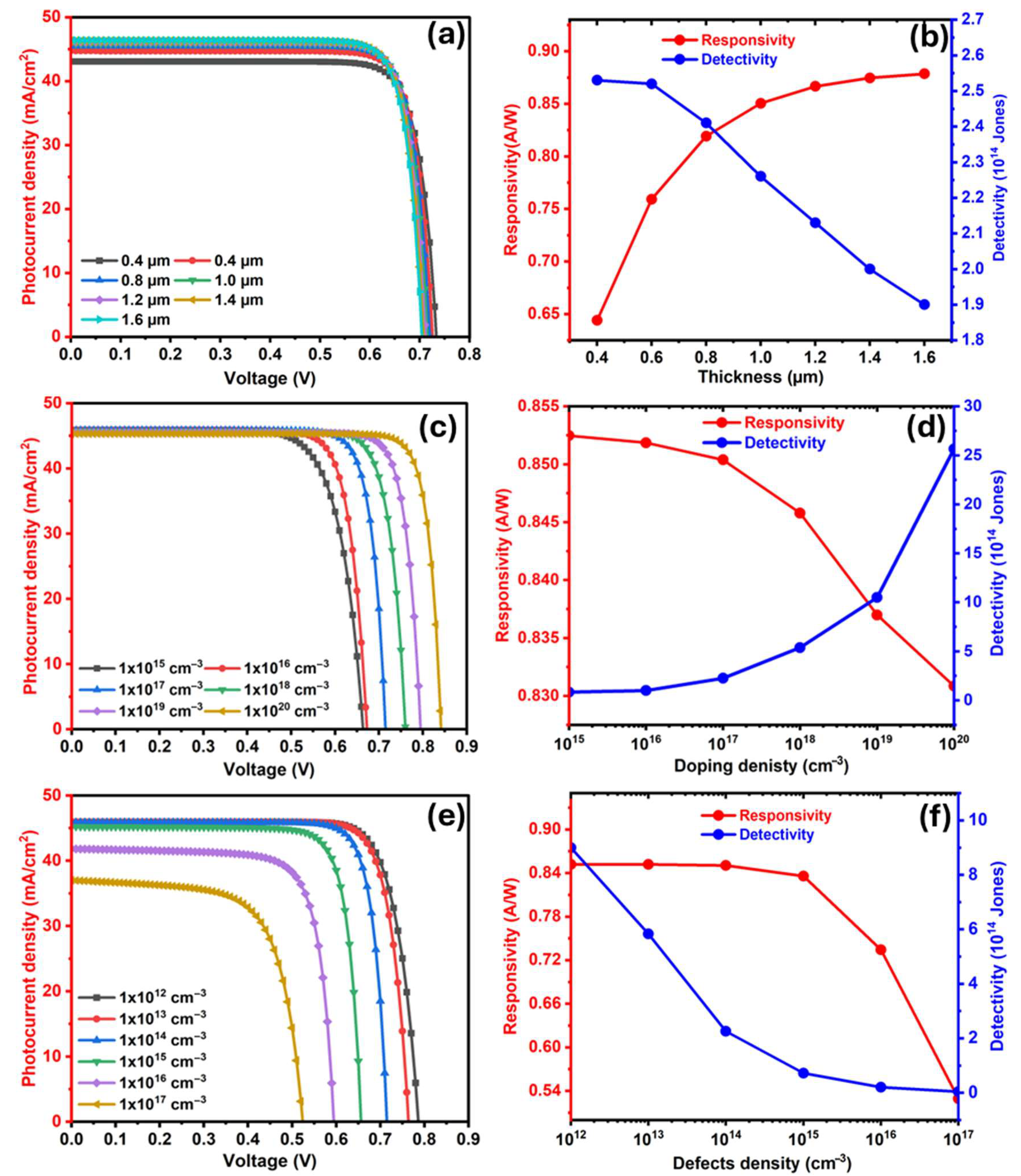
Figure 1a illustrates how varying the thickness of the SrHfSe3 absorber layer from 0.4 µm to 1.6 µm impacts key photodetector parameters, including Jsc, Voc, responsivity (R), and detectivity (D*). During this thickness-dependent analysis, both the doping density and defect level were fixed at 1018 cm−3 and 1014 cm−3, respectively. As depicted in Figure 2a, Jsc undergoes a noteworthy increase, rising from 43.07 mA/cm2 to 46.38 mA/cm2 as the absorber thickness increases. This enhancement is attributed to the increased light absorption in thicker layers, leading to greater photogeneration rates and, consequently, higher photocurrents [21]. Conversely, Voc steadily declines as thickness increases, dropping from 0.733 V to 0.704 V, likely due to enhanced bulk recombination in thicker layers, which lowers the carrier lifetime, as carriers tend to recombine before being extracted by the electrodes. Such behavior has also been reported in the literature [31].
The variation in the responsivity and the detectivity as the SrHfSe3 absorber thickness switches from 0.4 µm to 1.6 µm is delineated in Figure 1b. The amount of responsivity progressively increases from 0.644 A/W at 0.4 µm and reaches its upper limit at 0.879 A/W at 1.6 µm. This steady enhancement with the increase in the thin film width is ascribed to improved QE and enhanced photon-to-current conversion in thicker absorbers. This behavior of R is consistent with findings reported in the literature [42]. At the wavelength of 1100 nm, proximate to the bandgap edge of SrHfSe3, the responsivity attains its highest point of 0.85 A/W at an absorber thickness of 1 μm.
On the other hand, the detectivity follows a reverse behavior, peaking at its highest limit at 2.53 × 10¹⁴ Jones at 0.4 µm device’s thickness and then falling with increasing film thickness, eventually dropping to 1.9 × 10¹⁴ Jones at 1.6 µm as depicted in Figure 2b. This behavior can be ascribed to the simultaneous enhancement of QE with increasing absorber thickness, and the accompanying decline in photo-carrier collection efficiency as the layer becomes thicker [68]. In addition, the increase in recombination rate serves as the underlying reason for this effect, as demonstrated by Equation (10) [67], which shows that detectivity decreases with rising dark current. Under an incident wavelength of 1100 nm, a peak detectivity of 2.26 × 10¹⁴ Jones was attained when the absorber thickness was at its optimal value of 1 µm. Based on this analysis, it is important to highlight the trade-off between responsivity and detectivity as the absorber thickness varies. From an optimization standpoint, a SrHfSe3 thickness of 1.0 µm offers favorable device performance, with the photodetector achieving optimal characteristics, including a Jsc of 45.88 mA/cm2, a Voc of 0.7152 V, a responsivity of 0.85 A/W, and a detectivity of 2.26 × 10¹⁴ Jones making it a practical candidate for NIR photodetector applications.
Apart from the impact of the absorber thickness, the doping concentration of the absorber layer is a critical parameter that governs the electrostatic potential, carrier lifetime, and recombination dynamics within the photodetector. Therefore, its systematic analysis is necessary to optimize device performance and ensure efficient charge carrier transport with minimal recombination losses. In this investigation, both the thickness and the defect density of SrHfSe3 were fixed at 1 μm and 1 × 1014 cm−3, respectively. The doping density of SrHfSe3 was varied across a range from 1 × 10¹⁵ to 1 × 1020 cm−3 to clarify its impact on photodetector performance. Figure 2c reveals that at lower doping levels, from 1 × 10¹⁵ to 1 × 1017 cm−3, Jsc slightly decreases ranging from 45.92 to 45.88 mA/cm2. As the doping concentration increases to 1 × 10¹⁸ and 1 × 1019 cm−3, Jsc gradually decreases to 45.736 and 45.466 mA/cm2, respectively. Subsequently, Jsc noticeably drops until it reaches 45.317892 mA/cm2 at 1 × 1020 cm−3. This occurs because higher carrier concentrations within the absorber layer lead to increased carrier recombination rates [69]. In contrast, Voc shows a progressive improvement across the doping range. Specifically, it rises from 0.6639 to 0.7152 V as the doping density increases from 1 × 10¹⁵ to 1 × 1017 cm−3. With further increases in doping to 1 × 10¹⁸ and 1 × 1019 cm−3, Voc continues to improve, reaching 0.7603 and 0.7951 V, respectively. At 1 × 1020 cm−3, Voc significantly increases to 0.8417 V. The primary reason for the improvement in Voc is the reduction in the diode ideality factor and the increase in the built-in potential with an increase the doping density of the absorber layer, resulting in the increase in the Voc [70]. In addition, the increase in Voc may also be attributed to the decrease in the reverse saturation current, which results from the higher acceptor dopant concentration [31].
As shown in Figure 2d, the responsivity remains nearly constant at approximately 0.85 A/W for doping concentrations up to 1017 cm−3. However, it gradually decreases to around 0.83 A/W as the absorber doping level increases to 1020 cm−3. This decline is attributed to enhanced carrier recombination within the increasing the absorber layer doping level [64]. The maximum responsivity of 0.85 A/W is observed at the doping concentration of 1018 cm−3 at a wavelength of 1100 nm. In contrast, detectivity shows a consistent upward pattern with increasing doping, improving significantly from 0.84 × 10¹⁴ to 25.65 × 10¹⁴ Jones across the studied doping range. This enhancement is primarily due to the suppression of dark current and improved noise-limited sensitivity at higher doping levels. The increase in detectivity is closely related to the reduction in dark current, which is inversely proportional to Voc, as indicated by Equation (11). As Voc increases with doping, as previously observed, detectivity also improves [68]. This behavior is consistent with prior reports on chalcogenide-based photodetectors, such as TiS3 devices [64]. While extremely high doping levels can enhance both responsivity and detectivity, they present fabrication challenges and introduce trade-offs that can degrade overall device performance. Therefore, a doping concentration of 1 × 1017 cm−3 is identified as an optimal and practically feasible choice. At this level, the device demonstrates strong performance, including a Jsc of 45.88 mA/cm2, a Voc of 0.7152 V, a responsivity of 0.85 A/W, and a detectivity of 2.26 × 10¹⁴ Jones, without compromising manufacturability or long-term reliability.
Figure 2e illustrates the variation in Jsc and Voc of the SrHfSe3-based photodetector as the trap density of SrHfSe3 increases from 1 × 10¹² to 1 × 1017 cm−3, while maintaining a constant device thickness and doping level of 1 μm and 1 × 1017 cm−3, respectively. Both Jsc and Voc exhibit a consistent descending behavior with increasing trap concentration. At lower defect levels from 1012 to 1013 cm−3, Jsc remains nearly unchanged, decreasing only slightly from 45.96 to 45.95 mA/cm2, while Voc shows a minor reduction from 0.786 to 0.764 V. As the defect density increases to 1014 cm−3, Jsc declines modestly to 45.88 mA/cm2, accompanied by a more notable drop in Voc to 0.715 V. With further increases to 1015 and 1016 cm−3, Jsc decreases to 45.23 mA/cm2 and 41.83 mA/cm2, respectively, while Voc falls to 0.656 V and 0.595 V. At the highest defect density of 1017 cm−3, the device shows a sharp deterioration, with Jsc and Voc dropping to 36.99 mA/cm2 and 0.524 V, respectively.
Figure 2f displays the corresponding degradation in photoresponsivity and specific detectivity as the trap density increases across the same range. The device initially exhibits excellent performance at 1 × 1012 cm−3, with a responsivity of 0.85 A/W and detectivity of 9.0 × 10¹⁴ Jones, indicating efficient carrier collection and low noise levels. However, as the trap density rises, these values progressively decline. At 1 × 1017 cm−3, the responsivity reduces significantly to 0.53 A/W, while detectivity drops sharply to 0.0389 × 10¹⁴ Jones. This performance degradation across all parameters including Jsc, Voc, responsivity, and detectivity, is primarily attributed to enhanced trap-assisted recombination and increased dark current at higher defect densities, which was also observed in the previous studies [68,71]. To ensure high-efficiency operation, it is therefore essential to limit the trap density to the ideal values. A defect concentration of 1 × 1014 cm−3 is selected as the optimal trade-off point, where the device retains strong performance metrics, including Jsc = 45.88 mA/cm2, Voc = 0.7152 V, R = 0.85 A/W, and D = 2.26 × 10¹⁴ Jones.

3.2. The Impact of Window Layer (ZnSe) on the Photodetector Performance

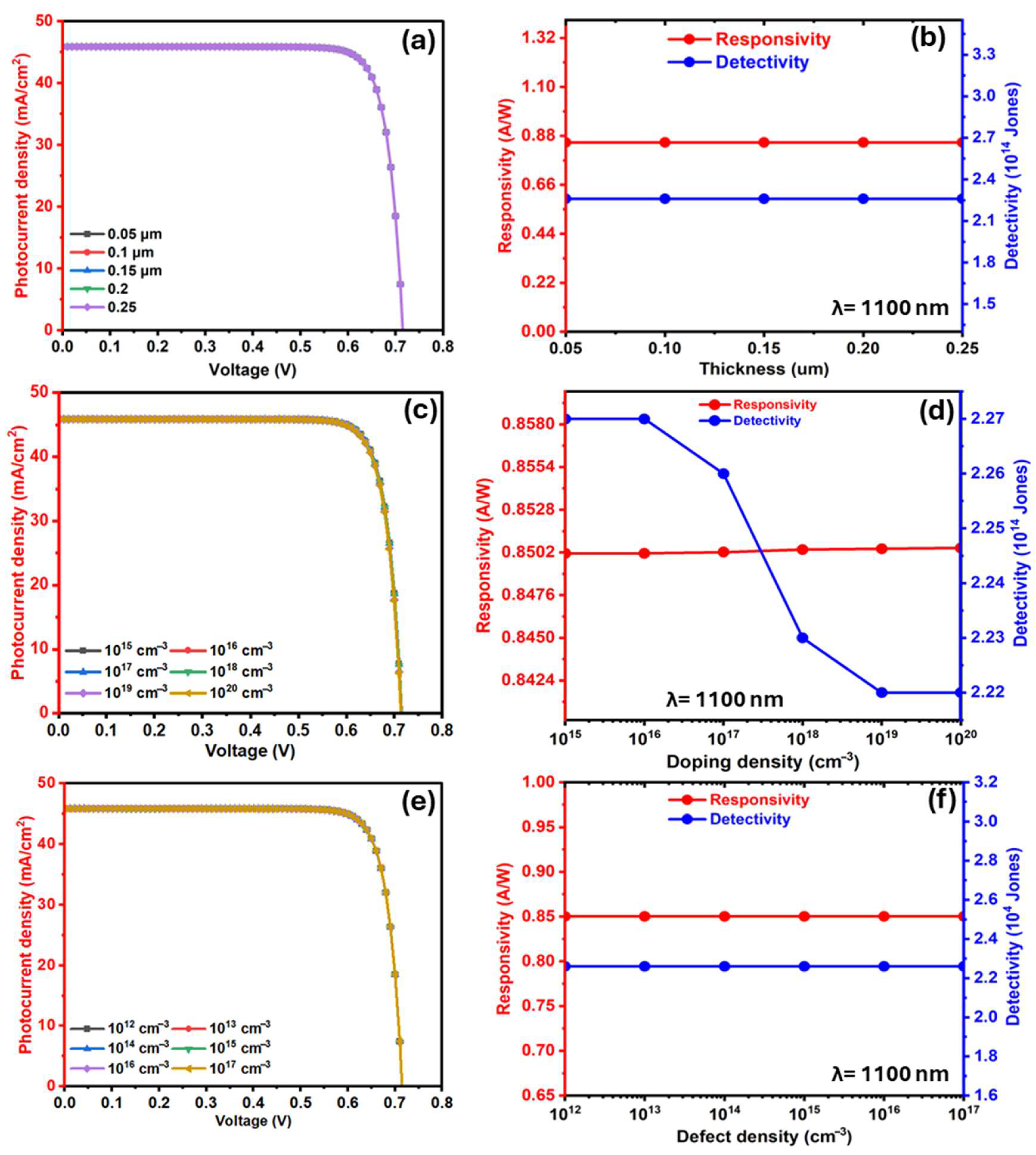
The effects of window layer ZnSe thickness on the photodetector performance were evaluated by varying its thickness from 0.05 µm to 0.25 µm, while fixing the doping and defect densities at 1018 cm−3 and 1015 cm−3, respectively. As shown in Figure 3a, both Jsc and Voc remain steady at 45.88 mA/cm2 and 0.7152 V, respectively, as the ZnSe thickness varies. This means that the light transmission and carrier collection are not impeded by the thickness. This behavior occurs due to the saturation in the optical absorption, as the diffusion length exceeds the layer thickness, leading to a reduction in recombination losses [64]. In the meantime, the fluctuation of the ZnSe thickness yielded no discernible changes in the responsivity and detectivity, which remained constant at 0.85 A/W and 2.26 × 10¹⁴ Jones, respectively, as shown in Figure 3b. This validates the performance metrics’ stability under different ZnSe thicknesses, which is in good agreement with the results reported in the literature [68]. Considering the performance uniformity under the ZnSe thickness variation, the thickness of 0.05 µm is chosen for further optimization, since it offers low cost, and enhanced transparency, all while maintaining high photodetector efficiency.
Figure 3c,d illustrate the influence of varying the ZnSe window layer doping density on the photodetector characteristics over the range from 1015 to 1020 cm−3. Figure 3a reveals that Jsc slightly increases with higher doping, rising from 45.88 to 45.89 mA/cm2, likely due to improved field-assisted carrier extraction, while Voc remains stable at 0.71 V as doping increases. Like the J-V characteristics, as shown in Figure 3d, the responsivity (red curve) remains unchanged at 0.85 A/W at 1100 nm incident light wavelength, with increasing doping levels. In contrast, the detectivity witnesses a slight reduction from 2.27 to 2.22 × 10¹⁴ Jones, likely due to increased dark current at higher doping concentrations. However, it remains relatively constant for doping concentrations below 1016 cm−3 and above 1018 cm−3. A moderate ZnSe doping density around 1018 cm−3 appears to strike a favorable balance between carrier collection and noise suppression, making it optimal for photodetector performance. At this doping level, the detectivity reaches 2.26 × 10¹⁴ Jones at a wavelength of 1100 nm.
The impact of defect density in the ZnSe window layer on the performance of the SrHfSe3-based photodetector is investigated by varying the defect density from 1012 to 1017 cm−3 while the thickness and the doping of ZnSe are fixed at the optimum level of 0.05 µm and 1018 cm−3, respectively. As shown in Figure 3e, Jsc remained independent of the defect density of the ZnSe, holding a value at 45.88 mA/cm2. Equally, the Voc maintains a stable value at 0.7152 V regardless of the defect concentration, reflecting stable junction quality and efficient carrier separation. Similarly, the responsivity and detectivity, as shown in Figure 3f, stay entirely unaffected by changes in the ZnSe defect density. The responsivity is constant at 0.85 A/W, while the specific detectivity holds stable at 2.26 × 10¹⁴ Jones. A ZnSe defect density of 1015 cm−3 appears to be an optimal value for achieving a favorable balance between carrier collection and recombination.

3.3. The Impact of the BSF Layer (AgCuS) on the Photodetector Performance

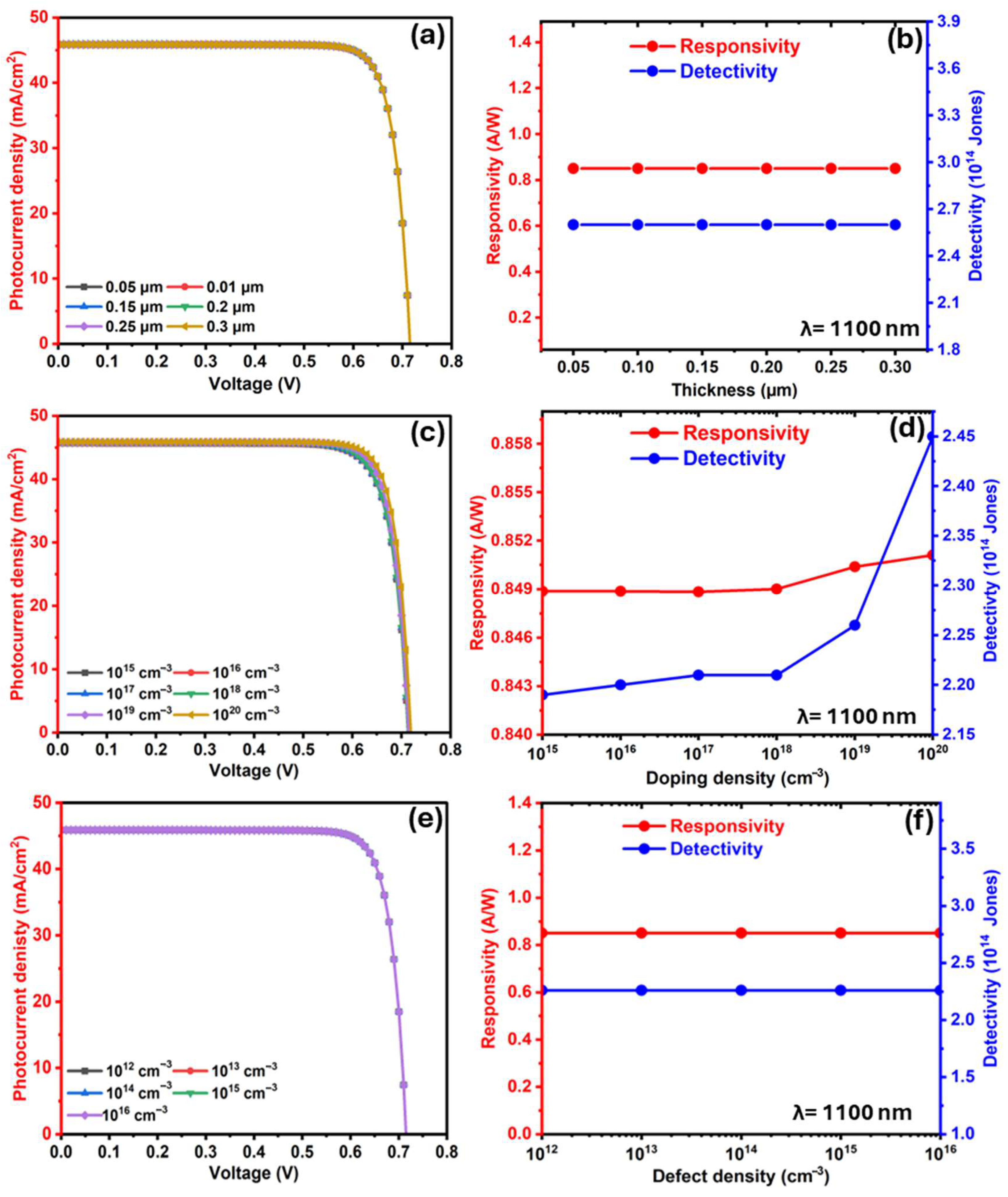
This section describes the influence of the BSF layer on the overall photodetector’s performance. Figure 4a,b illustrate the influence of AgCuS BSF layer thickness on photodetector characteristics as it varies from 0.05 µm to 0.30 µm, while other parameters are kept constant. As shown in Figure 4a, the J–V characteristics are nearly identical across the AgCuS thickness range, and the Voc remains constant at 0.7152 V. However, the Jsc exhibits a minor but consistent increase from 45.877 to 45.889 mA/cm2. This occurs since the carrier diffusion length exceeds the BSF thickness, preventing significant recombination losses [41]. Figure 4b further confirms a stable pattern in both responsivity at 0.85 A/W and detectivity at 2.6 × 10¹⁴ Jones, despite fluctuations in BSF thickness. The reason for such an unaffected performance is that the optical absorption reaches its saturation level, showing minimal improvement with further increases [68]. As the increase in Jsc becomes marginal beyond 0.20 µm and no further gains are observed in R and D, a BSF thickness of 0.20 µm is selected as the optimal value. It offers a balanced configuration with slight performance improvement without introducing unnecessary material usage or fabrication complexity.
Figure 4c,d assess the impact of doping concentration in the AgCuS BSF layer on the photodetector’s performance, with the BSF thickness fixed at 0.2 µm and the defect density maintained at 1015 cm−3 at 1100 nm light wavelength. As the doping density increases from 1015 to 1020 cm−3, Jsc rises from 45.674 to 45.911 mA/cm2, attributed to a stronger built-in electric field that enhances charge carrier separation and suppresses recombination at the back contact. Similarly, a slight improvement in Voc, from 0.7136 V to 0.7194 V, is observed. Likewise, the responsivity experiences a slight increase from 0.84 to 0.85 A/W, while the detectivity shows a more pronounced enhancement from 2.19 × 10¹⁴ to 2.45 × 10¹⁴ Jones at 1020 cm−3. At 1100 nm and a doping level of 1019 cm−3, an optimum detectivity of 2.26 × 10¹⁴ Jones, where the device can work without introducing resistive or recombination losses, and it can be practically achievable using standard doping methods. This pattern of responsivity and detectivity variation with increasing BSF layer doping concentration agrees with previously reported work [64]. At this doping level, the device exhibits Jsc, Voc, responsivity, and detectivity values of 45.88 mA/cm2, 0.7152 V, 0.85 A/W, and 2.26 × 10¹⁴ Jones, respectively.
Figure 4e,f shows the influence of defect density in the AgCuS BSF layer on the photodetector’s performance, keeping the BSF thickness at 0.2 µm and the doping concentration at 1019 cm−3. As shown in Figure 4e, the J-V characteristics remain almost perpetual as the defect density switches from 1012 to 1016 cm−3. The Voc holds a consistent value of 0.7152 V, and the Jsc holds steady at around 45.88 mA/cm2, indicating minimal impact of defect-related recombination within this range. Similarly, Figure 4f shows that both responsivity 0.85 A/W and detectivity 2.26 × 10¹⁴ Jones stay stable across all defect levels, further suggesting that carrier transport and collection in the AgCuS BSF layer are largely unaffected by moderate defect fluctuations. These findings are in strong agreement with prior reports [68]. As the device exhibits similar tolerance and performance robustness across a wide range of defect densities in the AgCuS BSF layer, a defect density of 1015 cm−3 can be considered a practical and fabrication-friendly choice. This level does not compromise efficiency and provides a solid foundation for further optimization.

3.4. The Impact of the Interfacial Defects on the Photodetector Performance

The density of interfacial defects plays a crucial role in determining the performance of heterojunction photodetectors, especially when there is a mismatch in lattice structure or energy levels between the absorber and contact layers. Therefore, a reasonable number of interface defects needs to be considered and analyzed as it impacts photodetector performance. Here, we explored how varying the interfacial defect density from 1 × 10⁸ to 1 × 1016 cm−3 affects the behavior of SrHfSe3-based photodetectors at the two different photodetector interfaces, including ZnSe/SrHfSe3 and SrHfSe3/AgCuS.
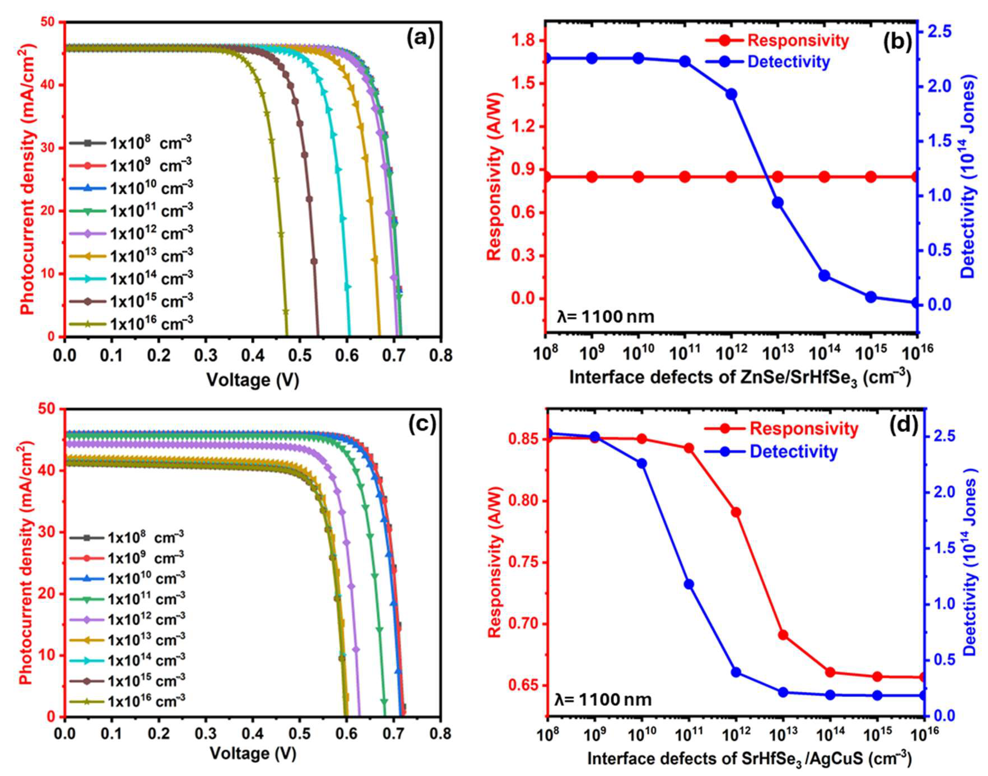
Figure 5a,b show the effect of variation in interfacial defect density at the ZnSe/SrHfSe3 junction on the photodetector performance. As shown in Figure 5a, the Jsc remains stable at 45.88 mA/cm2 up to 1013 cm−3, while Voc decreases significantly from 0.7152 V to 0.4726 V as the defect density increases from 108 to 1016 cm−3. This behavior results from enhanced carrier recombination and increased dark current due to the higher density of interfacial defects, both of which contribute to the reduction in Voc [51]. In terms of responsivity, its value remains constant at 0.85 A/W at 1100 nm across all defect levels. Unlike the responsivity, the detectivity holds steady at 2.26 × 10¹⁴ Jones up to 1010 cm−3 and then begins to noticeably degrade beyond 1012 cm−3, dropping to approximately 0.0207 × 10¹⁴ Jones at 1016 cm−3. This reduction is primarily attributed to the increase in dark current at higher interfacial defect densities. Thus, maintaining an interfacial defect density below 1011 cm−3 is critical for preserving low-noise and high-sensitivity performance at the front interface. Based on these findings, an interfacial defect density of 1010 cm−3 is selected as the optimal value for the ZnSe/SrHfSe3 interface for further optimization.
Figure 5c,d display the behavior of the photodetector performance with changes in the SrHfSe3/AgCuS interface, as the defect density increases from 108 to 1016 cm−3. As illustrated in Figure 5c, the Jsc decreases from 45.91 mA/cm2 at 108 cm−3 to 41.24 mA/cm2 at 1016 cm−3, reflecting a gradual reduction in carrier extraction efficiency. Similarly, the Voc drops from 0.721 V to 0.5969 V. The fall in both Jsc and Voc is attributed to the increasing defect density, which enhances charge carrier recombination at the SrHfSe3/AgCuS interface [72]. Unlike the ZnSe/SrHfSe3 interface, both responsivity and detectivity decrease adversely with increasing SrHfSe3/AgCuS interface defect densities. The responsivity remains nearly constant at 0.85 A/W up to 1010 cm−3 at 1100 nm, as depicted in Figure 5d. However, beyond 1011 cm−3, it significantly drops to 0.65 A/W at 1016 cm−3. Meanwhile, the detectivity remains stable at 2.26 × 10¹⁴ Jones up to 1010 cm−3, then exhibits a sharp decline, reaching 0.187 × 10¹⁴ Jones at 1016 cm−3. Compared with the ZnSe/SrHfSe3 interface, the SrHfSe3/AgCuS is more vulnerable to interfacial degradation, and to ensure high photodetector efficiency and low-noise operation, the SrHfSe3/AgCuS interface defect density must be maintained below 1011 cm−3. Consequently, a defect density of 1010 cm−3 is selected for SrHfSe3/AgCuS interface for further calculations.

3.5. The Impact of the Working Temperature on the Photodetector Performance

So far, all simulated calculations have been conducted at room temperature (300 K). However, to ensure stable and reliable photodetector performance, particularly for near-infrared applications operating in high-temperature environments, robust thermal management is critically important. Here, the simulated characteristics of the SrHfSe3-based photodetector across a temperature range of 300 K to 500 K are visualized in Figure 6. As shown in Figure 6a, the Jsc remains nearly constant, increasing only slightly from 45.88 to 45.96 mA/cm2, while the Voc gradually decreasing with rising temperature, dropping from 0.7152 V at 300 K to 0.4407 V at 500 K. This degradation is primarily caused by the amelioration in intrinsic carrier concentration and enhanced nonradiative recombination at higher temperatures, both of which contribute to the rise in the reverse saturation current and the subsequent drop in Voc [73].
Figure 6b shows the impact of altering the working temperature within a range from 300 K to 500 K on both responsivity and detectivity. The responsivity remains remarkably stable, obeying the Jsc pattern, increasing only slightly from 0.850 A/W at 300 K to 0.852 A/W at 500 K at 1100 nm. This signifies that the material maintains efficient photocarrier generation across variable temperatures. However, the D* exhibits a steep decline, dropping from its peak value of 2.26 × 10¹⁴ Jones at 300 K to just 1.12 × 10¹² Jones at 500 K. The rationale behind the sharp reduction in detectivity is mainly due to the elevated dark current at higher temperatures [71]. This increase in dark current may result from temperature-induced non-uniformities in device operation. Elevated temperatures can narrow the semiconductor bandgap, enhancing thermal carrier generation and thus increasing the dark current. This rise in dark current leads to a reduction in Voc, which is logarithmically and inversely related to dark current, as demonstrated by Equation (11). Working temperature variations may further cause spatial fluctuations in Voc, contributing to performance instability [31]. This behavior is in agreement with previous reports, which also observed stable responsivity and a decrease in detectivity with increasing operating temperature [51].
Figure 6c shows the impact of device working temperature on the dark current density. As the temperature increases from 300 K to 500 K, the dark current density undergoes a significant increase from 4.43 × 10⁻¹¹ to 1.81 × 10⁻⁶ mA/cm2. This severe increase suggests that more charge carriers are being thermally generated at higher temperatures, leading to increased leakage current in the device [41,62]. Figure 6d displays the on/off ratio as a function of the working temperature variation. A dramatic drop in the on/off ratio is observed, where the ratio drops from 1.04 × 10¹² at 300 K to 2.55 × 10⁷ at 500 K. This decline is mainly due to the increase in dark current, which reduces the contrast between the device’s light and dark states. As a result, the photodetector’s performance becomes less efficient at higher temperatures, indicating that its operation is strongly affected by thermal effects.

3.6. The Impact of the SrHfSe3 Bandgap Tuning on the Photodetector Performance

To gain more qualitative insights, we investigate how Sb-doping affects the band gap of the SrHfSe3 layer and, in turn, the device’s electrical characteristics. Pristine SrHfSe3 has a direct band gap of approximately 1.00–1.02 eV. When doped with Sb, the band gap increases to 1.06 eV at 0.5 mol % and to 1.15 eV at 1.0 mol %, as confirmed by both density functional theory (DFT) calculations and experimental data [39]. The direct band gap makes SrHfSe3 suitable for near-infrared photodetectors, and Sb doping enhances its response across a broader wavelength range. This spectral tunability highlights Sb-doping as a promising strategy for developing photodetectors with broad spectral sensitivity.
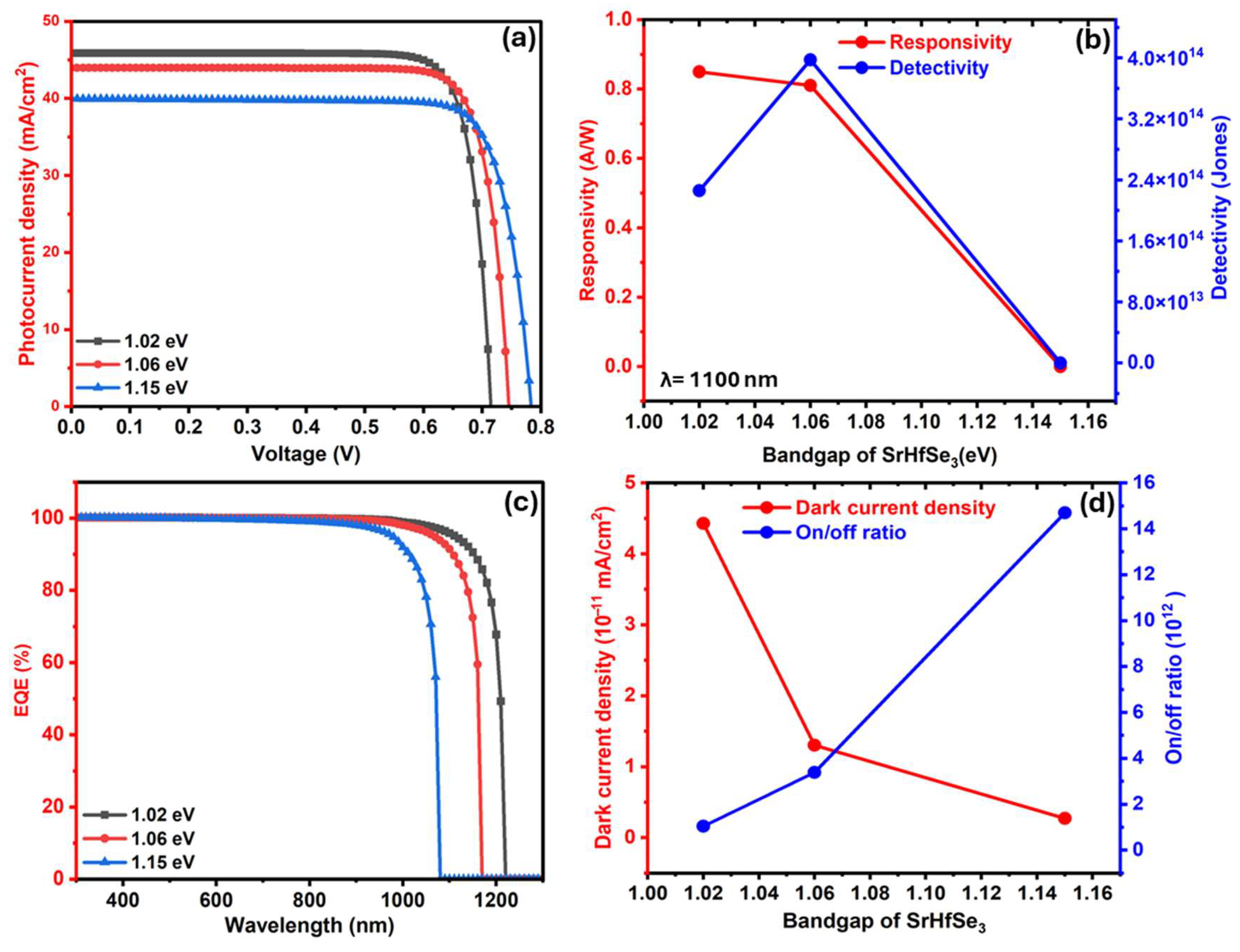
The photodetector characteristics with the alteration of SrHfSe3 bandgap from 1.02 eV to 1.15 eV are shown in Figure 7. As shown in Figure 7a, the J–V characteristics reflect a clear dependence of Jsc and Voc on bandgap energy. At 1.02 eV, the device achieves the highest Jsc of around 45.88 mA/cm2 due to stronger near-infrared (NIR) light absorption. However, the Voc is lower in this case, likely due to increased carrier recombination or a weaker built-in electric field. Increasing the bandgap to 1.06 eV leads to a modest drop in Jsc (44.39 mA/cm2), but Voc significantly improves due to enhanced carrier separation and suppressed recombination. At 1.15 eV, photocurrent drops further to 39.92 mA/cm2 despite a higher Voc, indicating reduced photon absorption as the cutoff shifts away from the 1100 nm operating wavelength.
Figure 7b presents the impact of bandgap variation on responsivity and specific detectivity. The highest responsivity of 0.85 A/W occurs at 1.02 eV, in line with the stronger photocurrent. At 1.06 eV, responsivity slightly decreases to 0.81 A/W, but detectivity peaks at 3.97 × 10¹⁴ Jones due to an optimal balance between signal and dark noise. The noticeable drop in responsivity and detectivity at a bandgap of 1.15 eV is closely linked to the device’s quantum efficiency at 1100 nm. As shown in Figure 7a, the EQE plot, the 1.15 eV structure exhibits a much earlier cutoff compared to the 1.02 eV and 1.06 eV cases, which maintain high quantum efficiency near this wavelength. Since fewer photons are absorbed at 1100 nm when the bandgap is too large, the resulting photocurrent drops significantly. This loss in signal directly reduces responsivity and ultimately degrades detectivity. In contrast, the 1.06 eV configuration sustains strong EQE at 1100 nm, explaining its peak detectivity. However, as depicted in Figure 7c, the EQE remains relatively stable across the wavelength range, showing only minor fluctuations at longer wavelengths [74].
Figure 7d illustrates the impact of bandgap energy on the dark current density and on/off ratio of the proposed photodetector. As the bandgap increases from 1.02 eV to 1.15 eV, a clear inverse relationship is observed between dark current and the on/off ratio. At 1.02 eV, the device exhibits a relatively high dark current density of 4.43 × 10⁻¹¹ mA/cm2, accompanied by a modest on/off ratio of 1.04 × 10¹². This elevated dark current can be attributed to the narrower energy gap, which facilitates thermal generation of carriers and leakage pathways under dark conditions. As the bandgap widens to 1.06 eV, the dark current significantly decreases to 1.72 × 10⁻¹¹ mA/cm2, while the on/off ratio improves to 2.57 × 10¹², indicating enhanced discrimination between photo and dark currents. Notably, at 1.15 eV, the dark current reaches its lowest value of 2.71 × 10⁻¹² mA/cm2, while the on/off ratio peaks at 1.47 × 10¹³. This substantial improvement reflects the suppressive effect of a wider bandgap on thermally induced carrier excitation, thereby enhancing signal clarity and noise immunity. Overall, these results highlight that increasing the bandgap of the absorber layer effectively suppresses dark current while significantly enhancing the photodetector’s switching performance, making it highly suitable for high-sensitivity and low-noise optoelectronic applications.
Overall, the results highlight the importance of bandgap engineering in optimizing device performance. From an application perspective, a bandgap of around 1.02 eV is best suited for SrHfSe3 photodetectors targeting near-infrared operation, while 1.06 eV offers optimal performance for self-powered or low-light conditions. Therefore, a 1.02 eV bandgap is selected for further calculations.

3.7. The Impact of the Change in the Input Power on the Phototodetector Performance

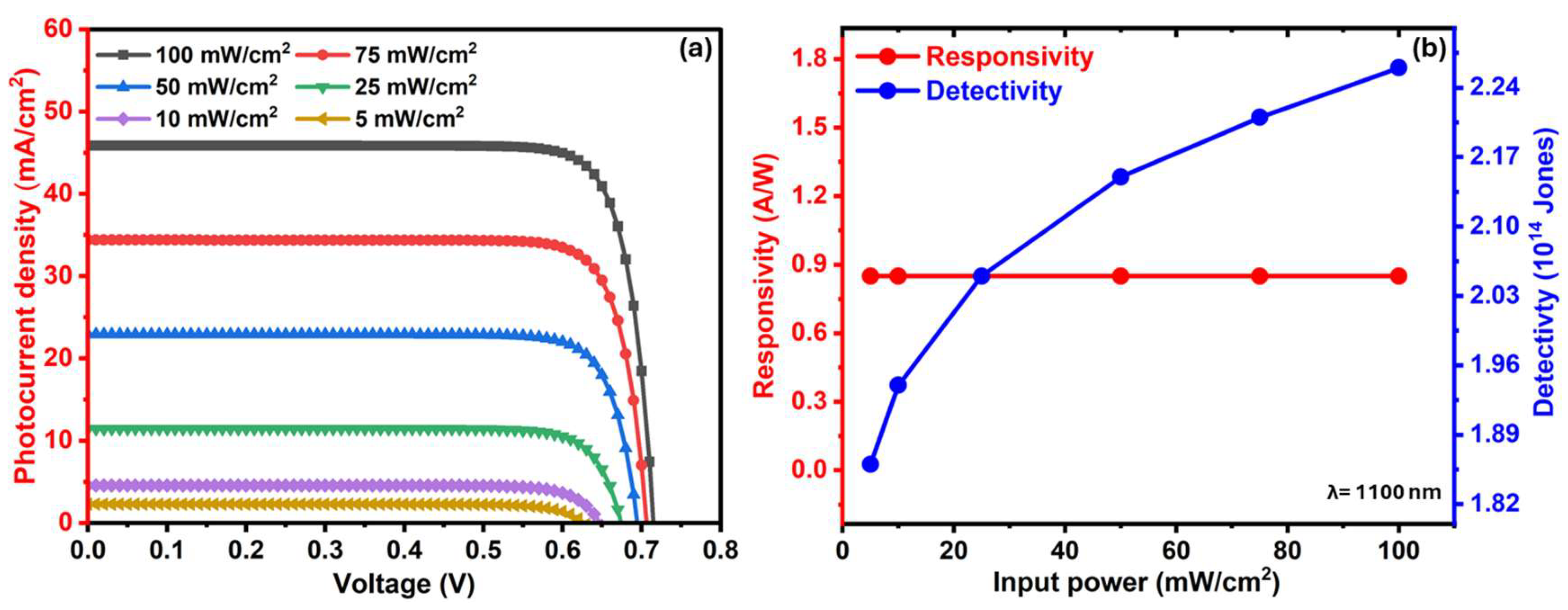
So far, all simulations were primarily carried out under a standard illumination intensity of 100 mW/cm2. However, to rigorously assess the light-intensity-dependent behavior of the device and highlight the critical limitations of the SrHfSe3-based photodetector, the variation in Jsc, Voc, responsivity, and detectivity with increasing illumination was further explored, as illustrated in Figure 6. As displayed in Figure 6a, it is revealed that as the light intensity rises from 5 mW/cm2 to 100 mW/cm2, Jsc exhibits a substantial rise from 2.29 mA/cm2 to 45.89 mA/cm2. This enhancement is primarily due to the elevated photon flux, which increases the generation rate of charge carriers. The relationship between Jsc and incident power (P) follows a power-law behavior, given by Jsc ∝ P^α, where α typically ranges from 0.9 to 1.0 in ideal photodiodes, indicating a near-linear dependence [75]. Similarly, Voc evolves from 0.6275 V to 0.7152 V as the illumination intensity increases. This improvement is attributed to the enhancement of the built-in electric field and the suppression of carrier recombination, leading to more efficient charge separation. The overall behavior is consistent with classical photodiode operation, where Jsc scales nearly linearly while Voc exhibits a logarithmic dependence on input power, in agreement with a previously reported simulation-based study [64].
Figure 8b illustrates the behaviors of responsivity (R) and detectivity (D*) with illumination power. The responsivity remains almost constant at approximately 0.85 A/W across the optical power range. On the other hand, detectivity gradually optimized from 1.86 × 10¹⁴ to 2.26 × 10¹⁴ Jones as the input power increases. This likely results from a reduced signal-to-noise ratio at higher optical power, combined with saturation effects and dynamic range limitations of the photodetector. These findings align well with the previously reported work [64].

3.8. The Impact of the Series, Shunt Resistance, and Electron Affinity on the SrHfSe3 Photodetector Performance

The influence of series and shunt resistances on Voc and Jsc is depicted in Figure 9a,b, respectively. The series resistance originates from the body and the contact, while the shunt resistance typically stems from fabrication flaws and reverse leakage current [76]. Consequently, controlling both parameters, especially the series resistance, is crucial for enhancing photodetector performance. Figure 9a shows the fluctuation of Voc and Jsc with increasing series resistance from 0 to 20 Ω. As the resistance increases, Voc remains nearly constant at nearly 0.71 V. On the contrary, Jsc stays perpetual at 45.88 mA/cm2 up to 4 Ω. Subsequently, it drops sharply at 16 Ω to 40.71 mA/cm2 and further decreases to 33.80 mA/cm2 at 20 Ω. This reduction in Jsc is likely due to increased resistive losses, which impede carrier collection and thereby suppress the short-circuit current. This can be further explained by the following Equation (12) [62]:
J p = J L + J 0 e V o c q n k T 1 V o c + J p R S R S h
where the J p , R S h , R S , J L , and J 0   represent the photocurrent, shunt resistance, series resistance, light-generated current, and reverse saturation current, respectively. As can be observed from the equation, an increase in series resistance leads to a reduction in the photocurrent.
Apart from the series resistance, the impact of shunt resistance on Voc and Jsc is also studied, as shown in Figure 9b. It is observed that both Voc and Jsc exhibit stable trends as the shunt resistance increases from 1 to 20 kΩ, maintaining values around 0.7152 V and 45.88 mA/cm2, respectively. Figure 9c,d display the Voc and Jsc dependent on the electron affinity of the SrHfSe3-based photodetector, respectively. As the electron affinity increases from 3.9 eV to 4.4 eV, the Voc gradually drops from 0.7152 V to 0.6035 V. The reason for this decline may likely result from less favorable band alignments between the photodetector layers that reduce the built-in potential and increase recombination losses. Concurrently, the Jsc shows a slight variation with the increase in electron affinity. It marginally decreases from 44.89 to 44.4 mA/cm2 as the electron affinity increases from 3.9 to 4.0 eV, and then rises, reaching a peak value of 45.90 mA/cm2 at 4.3 eV. The value of 3.9 eV appears to be the optimal point at which the detector exhibits both high Voc and Jsc, and can thus be used for further calculations.

3.9. The Built-In Potential of the Photodetector

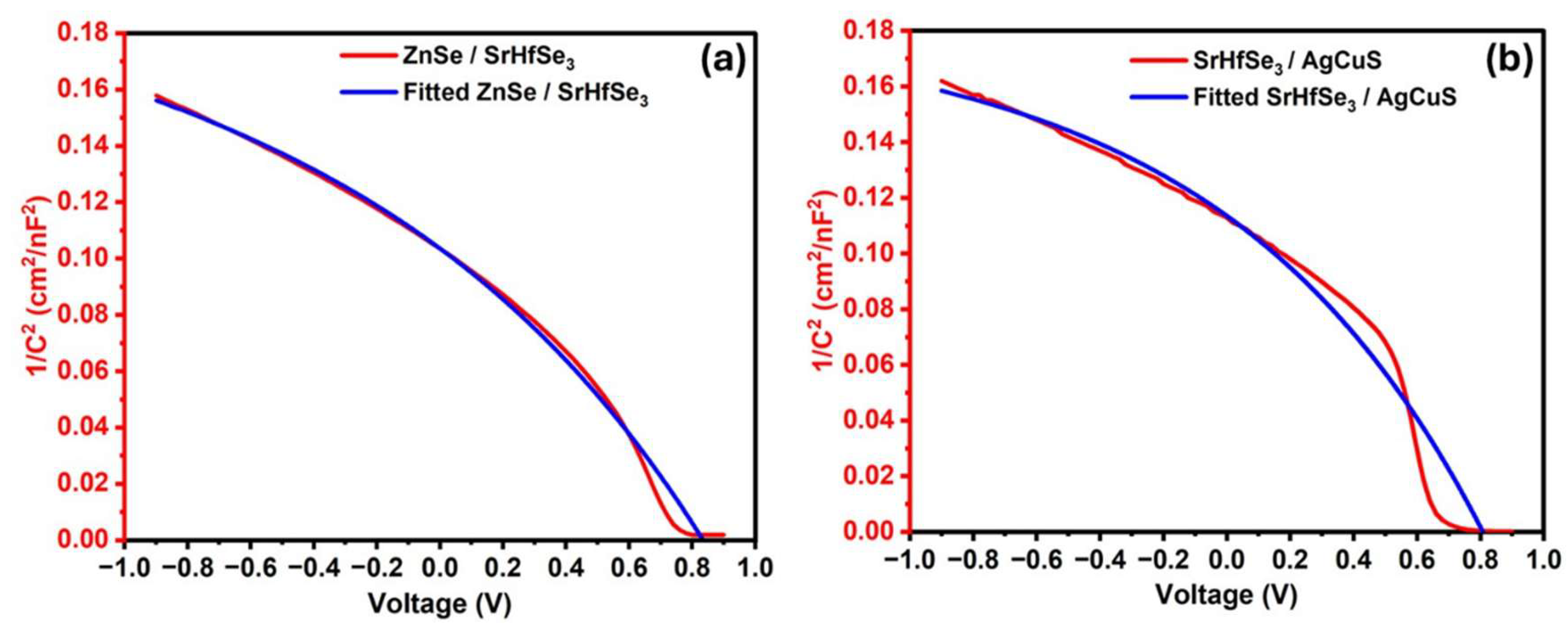
The built-in potential (φbi) across the device heterojunctions plays a critical role in enhancing the internal electric field and promoting efficient charge separation and extraction. It can be estimated from the intercept of the Mott–Schottky (1/C)2–V plot as illustrated by Equation (13) [55].
1 C 2 = c K T q b i V q A 2 ε 0 ε S r H f S e 3 N D
Here, ε S r H f S e 3 and ε0 denote the permittivity of SrHfSe3 and vacuum, respectively. The C denotes the capacitance at the junction, and V is the applied voltage. The N D represents the donor concentration, q is the elementary charge (1.6 × 10⁻¹⁹ C), and A corresponds to the diode’s active area.
Figure 10a,b presents the plots of 1 C 2 versus voltage for the heterojunctions ZnSe/SrHfSe3 and SrHfSe3/AgCuS, respectively. The red curves in both figures represent simulation results obtained using the SCAPS-1D (3.3.12) software, while the blue curves correspond to the fitted data derived using OriginPro 2025 software to extract the built-in potential. To determine the effective built-in potential of the entire system, the built-in voltages from each junction were individually extracted from the interceptions of the linear portions of the fitted curves on the voltage axis. These values are found to be 0.82 V for the ZnSe/SrHfSe3 junction and 0.81 V for the SrHfSe3/AgCuS junction. Summing these values yield a total built-in potential of approximately 1.63 V for the complete device architecture.
The relatively high total potential can be attributed to the well-aligned energy bands at the ZnSe/SrHfSe3 and SrHfSe3/AgCuS interfaces, which facilitate efficient charge separation and transport across the heterojunctions.

3.10. The Optimized Design with and Without the BSF Layer

Figure 11a shows the impact of adding a BSF layer between SrHfSe3 and the back contact Cu on the photodetector performance. It is evident that the installation of an AgCuS (BSF) layer into the photodetector structure substantially boosts the overall performance. As shown in Figure 11a, the device yields a Jsc of 41.31 mA/cm2 and a Voc of 0.5975 V without the AgCuS layer. Upon addition of the AgCuS BSF, the Voc grows to 0.7152 V, and Jsc jumps to 45.88 mA/cm2. With respect to the EQE, adding the BSF layer into the photodetector design enhanced the EQE in the 300 to 1200 nm range, retaining almost 100% up to 830 nm as depicted in Figure 11b. Beyond this wavelength, it gradually declined, approaching nearly zero over 1210 nm.
The wavelength-dependent spectral responsivity and detectivity are depicted individually in Figure 11a,d. As shown in Figure 11b, the spectral responsivity rises with the inclusion of the BSF layer, attaining its highest value of around 0.85 A/W at 1100 nm. Conversely, without a BSF layer, the summit responsivity is shifted to around 1040 nm, where it attains a lower maximum of 0.675 A/W.After this peak, the response drops with growing wavelength for both configurations with and without the BSF layer, ultimately approaching zero beyond 1210 nm.
In addition, as shown in Figure 11d, the integration of the BSF layer leads to an increase in the detectivity, reaching a dominant peak value of 2.26 × 10¹⁴ Jones at 1100 nm. This significantly surpasses the detectivity of the configuration without the BSF layer, which peaks at around 1.94 × 10¹³ Jones at 1040 nm. The underlying physics behind this enhancement is that adding the AgCuS BSF layer improves detector performance from 400 to 1100 nm by enhancing light absorption and increasing Jsc, which is directly linked to responsivity. Adding a Back Surface Field (BSF) layer forms a dual junction, typically an n/p or p/p+ structure, that enhances the built-in potential within the device. This improved junction configuration helps reduce dark current collection, thereby increasing the Voc. The increase in Voc is associated with a reduction in dark current, as shown in Equation (14) [31].
V o = k B T q l n J s c J 0
In addition, the BSF layer reduces recombination losses by reflecting incident photons, which further improves Voc and results in better detectivity, as demonstrated in Equation (10) [67,68].
As shown in Table 4, the incorporation of the AgCuS layer significantly enhances the overall efficiency of the device. Notably, both the spectral responsivity and detectivity reach their peak values with the inclusion of the BSF layer, observed at different wavelengths of 1100 nm and 1040 nm, respectively.

3.11. Performance Comparison

Table 5 presents a comprehensive comparison of the photoresponse characteristics reported in various experimental and simulation-based photodetector studies, including the results from our current work. Notably, various reported work was conducted using the SCAPS-1D simulation software, which further validates its reliability and versatility in modeling diverse photodetector structures. This comparison highlights SCAPS-1D as an efficient and accessible tool for simulating a wide range of device architectures, including Schottky, pn, and pin configurations, such as the one implemented in our design. It is worth mentioning that the reported photoresponsivity and photosensitivity values correspond to their peak values, which are wavelength-dependent and influenced by various device factors.
The table also includes experimental devices such as the Si:S photodetector, which demonstrates a trade-off between scalability and performance. Fabricated via ion implantation and annealing, the device offers CMOS compatibility but exhibits limited responsivity (0.1073 A/W). The table also includes compounds containing elements such as Cd and Pb, which are well known for their toxicity and raise significant environmental and health concerns. Regardless of their performance, materials containing Ge, In, and Te are associated with high costs due to their limited availability in the Earth’s crust. The responsivity reported in these works is relatively low compared to our device performance, except in the cases of BeSiP2 and TiSe2, MoS2, Ag3CuS2, and Gr/GaAs photodetectors. In addition, the performance of these devices is limited to wavelengths around 1000 nm and shows poor response beyond 1100 nm due to their relatively wide bandgap.
Apart from exhibiting high performance, the photodetector is primarily composed of SrHfSe3 as the main absorber material. This compound consists of strontium (Sr), hafnium (Hf), and selenium (Se), elements that are relatively earth-abundant and less toxic compared to those used in conventional semiconductors. Their availability and environmental compatibility make SrHfSe3 a promising choice for sustainable optoelectronic applications [39,77,78].
Table 5. Comparison of the proposed photodetector with the literature work.
StructureTypes of Workλ(nm)Software Used
/Method
Responsivity (A/W)Detectivity (Jones)Reference
Si:SExperimental1310 Ion implantation + rapid thermal annealing 0.1073-[79]
p-WSe2/n-Ge Experimental1550Mechanical exfoliation + Ion implantation 1.3 2.5 × 10¹⁰[80]
InGaAs/InAsExperimental1550
2000
CVD0.6 at 1550 nm
15 at 2000 nm
2.4 × 10¹⁴
3.8 × 10¹⁰
[11]
p-n GeSimulation1550Lumerical Change FDTD0.43-[47]
Graphene/GaAsSimulation725 COMSOL
Multiphysics
0.5141.16 × 1011[81]
InGaAs/InAs/InSb/InP HEMTSimulation900–1700 TCAD Silvaco15.75 4.0384 × 1010[49]
p-MoS2Simulation700 SCAPS-1D0.373.27 × 1014[82]
n-CdS/p-Cu2ZnGeSe4/p+-ZnTeSimulation780 SCAPS-1D0.58 8.28 × 10¹⁷[46]
PbS/TiS3Simulation780 SCAPD 1D0.36 3.9 × 10¹³[4]
n-ZnSe/p-TiSe2/p+-WSe2Simulation920 SCAPS 1D0.67012.90 × 1014[41]
n-In2S3/p-BeSiP2/p+-MoS2Simulation860 SCAPS 1D0.643.63 × 1016[67]
n-WS2/p-Ag3CuS2/p+-BaSi2Simulation1065 SCPDS 1D0.7904.73 × 1014[63]
n-ZnSe/p-SrHfSe3/p+-AgCuSSimulation1100 SCAPS-1D0.8502.26 × 1014This work

4. Conclusions

This study has designed and simulated a photodetector based on n-ZnSe/p-SrHfSe3/p+-AgCuS using SCAPS-1D. Various parameters were thoroughly evaluated and optimized, including the energy bands, J–V curves, photoresponsivity, and specific detectivity. To optimize the photodetector performance, many factors such as the thickness, defects, and the doping density for each layer of the device were precisely optimized. In addition, the interface defects, bandgap of the main absorber, working temperature, and input light intensity were also evaluated to optimize the proposed design further. The optimized parameters consist of a 1 µm thick absorber layer, a 0.05 µm window layer, and a 0.200 µm thick BSF layer. The doping densities for the absorber, window layer, and BSF layer are found to be 1017 cm−3, 1018 cm−3, and 1019 cm−3, respectively. The optimized device displayed a photocurrent of 45.88 mA/cm2 and a voltage of 0.7512 V at room temperature (300 K). Under a light wavelength of 1100 nm, the simulated photodetector shows off a photoresponsivity of 0.85 A/W and a detectivity of 2.26 × 10¹⁴ Jones. The optimized interface defect level was found to be 1010 cm−2 for both n-n-ZnSe/p-SrHfSe3 and n-ZnSe/p-SrHfSe3/p+-AgCuS interfaces. In addition, the device displayed a better spectral photoresponse in the 700–1200 nm range, with the highest photoresponse attained at 1100 nm, indicating suitability for near-infrared detection. Finally, compared to previous strategies reported in the literature, this device demonstrates significant promise for research areas that require high-performance and stable photodetectors. Its high responsivity and detectivity significantly reinforce its potential for next-generation photodetector applications.

Author Contributions

Conceptualization and methodology, S.A. (Salah Abdo); software, S.A. (Salah Abdo); validation, A.E.M.; formal analysis, S.A. (Salah Abdo); investigation, S.A. (Salah Abdo), A.A.O. and S.A. (Sanjida Akter); resources, S.A. (Salah Abdo); writing—original draft preparation, S.A. (Salah Abdo) and A.A.O.; writing—review and editing, S.A. (Salah Abdo); A.A., K.A. and A.A.O.; visualization, S.A. (Salah Abdo); supervision, H.H.; supervision, N.K. and A.E.M. All authors have read and agreed to the published version of the manuscript.

Funding

This research was funded through the Australian Research Council Discovery Project grant (DP200101353).

Institutional Review Board Statement

Not applicable.

Data Availability Statement

The data that support the findings of this study are available from the corresponding author upon reasonable request.

Acknowledgments

The authors sincerely thank Marc Burgelman from the University of Gent, Belgium, for sharing the SCAPS (Solar Cell Capacitance Simulator).

Conflicts of Interest

The authors declare no conflicts of interest.

Abbreviations

The following abbreviations are used in this manuscript:
AgCuSsilver copper disulfide
CBMconduction band minimum
EC/EVenergy level of the conduction/valence band
ETL/HTLelectron/hole transport layer
Egbandgap
HgCdTemercury cadmium telluride
InGaAsindium gallium arsenide
JSCshort-circuit current density
J–Vcurrent voltage
NIRnear infrared
Ntdefect density
PDsphotodetectors (PDs)
QEquantum efficiency
Rsseries resistance
Rshshunt resistance
SCAPS-1Dsolar cell capacitance simulator one-dimension
SrHfSe3strontium hafnium selenide
VBMvalence band maximum
VOCopen-circuit voltage
Vbibuilt-in potential
ZnSezinc sulfide

References

  1. Lee, J.-J.; Han, S.-J.; Hwang, D.K. Understanding Photoinduced Memory Effects in Optoelectronic Devices across Photoresponse Time Scales for Sensor-Based Artificial Intelligence. ACS Photonics 2025, 12, 2262–2278. [Google Scholar] [CrossRef]
  2. Kumar, A.; Chakkar, A.G.; Das, C.; Kumar, P.; Sahu, S.; Saliba, M.; Kumar, M. Self-Powered Broadband Photodetectors Based on WS2-Anchored MoS2 with Enhanced Responsivity and Detectivity. Small 2025, 21, 2502900. [Google Scholar] [CrossRef]
  3. Roy, N. Investigating Cs2SnI6 as a promising material for high-performance self-powered broadband photodetection application. J. Phys. Chem. Solids 2025, 203, 112730. [Google Scholar] [CrossRef]
  4. Yao, H.; Liu, L. Design and optimize the performance of self-powered photodetector based on PbS/TiS3 heterostructure by SCAPS-1D. Nanomaterials 2022, 12, 325. [Google Scholar] [CrossRef] [PubMed]
  5. Mahato, S.; Tamulewicz-Szwajkowska, M.; Singh, S.; Kowal, D.; Bose, S.; Serafińczuk, J.; Czyż, K.; Jędrzejewski, R.; Birowosuto, M.D.; Ray, S.K.; et al. Surface-Engineered Methylammonium Lead Bromide Single Crystals: A Platform for Fluorescent Security Tags and Photodetector Applications. Adv. Opt. Mater. 2024, 12, 2302257. [Google Scholar] [CrossRef]
  6. Abdo, S.; As’ ham, K.; Odebowale, A.A.; Akter, S.; Abdulghani, A.; Al Ani, I.A.; Hattori, H.; Miroshnichenko, A.E. A Near-Ultraviolet Photodetector Based on the TaC: Cu/4 H Silicon Carbide Heterostructure. Appl. Sci. 2025, 15, 970. [Google Scholar] [CrossRef]
  7. Srivastava, R.; Verma, S.; Chaudhary, A.K.; Sahu, A. Enhanced red light detection in eco-friendly perovskite-based photodetector with improved low-light sensitivity. Solid State Commun. 2025, 403, 115983. [Google Scholar] [CrossRef]
  8. Yasin, S.; Christopoulos, S.; Abu Waar, Z.; Moustafa, M. Numerical Modeling and Optimization of High-Performance CsSnI3 Perovskite Photodetectors. J. Electron. Mater. 2025, 54, 5690–5700. [Google Scholar] [CrossRef]
  9. Chen, B.; Xu, J.; Shi, S.; Kong, L.; Zhang, X.; Li, L. UV–Vis–NIR Broadband Self-Powered CuInS2/SnO2 Photodetectors and the Application in Encrypted Optical Communication. ACS Appl. Mater. Interfaces 2024, 16, 28917–28927. [Google Scholar] [CrossRef] [PubMed]
  10. Chen, J.; Zhang, Z.; Ma, Y.; Feng, J.; Xie, X.; Wang, X.; Jian, A.; Li, Y.; Li, Z.; Guo, H.; et al. High-performance self-powered ultraviolet to near-infrared photodetector based on WS2/InSe van der Waals heterostructure. Nano Res. 2023, 16, 7851–7857. [Google Scholar] [CrossRef]
  11. Woo, S.; Yeon, E.; Ryu, H.Y.; Han, J.H.; Jang, H.W.; Jung, D.; Choi, W.J. High Detectivity Dual-Band Infrared Photodetectors with Dislocation-Assisted Photoconductive Gain via Hetero-Epitaxial Growth. Adv. Funct. Mater. 2025, 35, 2419329. [Google Scholar] [CrossRef]
  12. Wang, Y.; Gu, Y.; Cui, A.; Li, Q.; He, T.; Zhang, K.; Wang, Z.; Li, Z.; Zhang, Z.; Wu, P.; et al. Fast uncooled mid-wavelength infrared photodetectors with heterostructures of van der Waals on epitaxial HgCdTe. Adv. Mater. 2022, 34, 2107772. [Google Scholar] [CrossRef] [PubMed]
  13. Li, Q.; Guo, Y.; Liu, Y. Exploration of near-infrared organic photodetectors. Chem. Mater. 2019, 31, 6359–6379. [Google Scholar] [CrossRef]
  14. Guo, Z.; Wang, J.; Du, J.; Wu, D.; Zeng, L.; Tsang, Y.H.; Wu, D.; Wang, Y.; Ding, Y.; Lin, P. Self-driven Te0.65Se0.35/GaAs SWIR photodiode with spectral response to 1.55 μm for broadband imaging and optical communication. Nano Energy 2025, 133, 110452. [Google Scholar] [CrossRef]
  15. Liu, C.; Guo, J.; Yu, L.; Li, J.; Zhang, M.; Li, H.; Shi, Y.; Dai, D. Silicon/2D-material photodetectors: From near-infrared to mid-infrared. Light Sci. Appl. 2021, 10, 123. [Google Scholar] [CrossRef]
  16. Liu, X. Highly strained Ge nanostructures and direct bandgap transition induced by femtosecond laser. Semicond. Sci. Technol. 2025, 40, 045013. [Google Scholar] [CrossRef]
  17. Zhang, X.; Shao, J.; Du, S.; Lu, T.; Wang, Y.; Wang, F.; Geng, Y.; Tang, Z. Ultra-broadband, self-powered and high performance vertical WSe2/AlOx/Ge heterojunction photodetector with MXene electrode. J. Alloys Compd. 2023, 930, 167484. [Google Scholar] [CrossRef]
  18. Son, B.; Lin, Y.; Lee, K.H.; Chen, Q.; Tan, C.S. Dark current analysis of germanium-on-insulator vertical pin photodetectors with varying threading dislocation density. J. Appl. Phys. 2020, 127, 203105. [Google Scholar] [CrossRef]
  19. Wang, J.; Chen, J. High-sensitivity silicon: PbS quantum dot heterojunction near-infrared photodetector. Surf. Interfaces 2022, 30, 101945. [Google Scholar] [CrossRef]
  20. Peng, L.; Wang, Y.; Ren, Y.; Wang, Z.; Cao, P.; Konstantatos, G. InSb/InP Core–Shell Colloidal Quantum Dots for Sensitive and Fast Short-Wave Infrared Photodetectors. ACS Nano 2024, 18, 5113–5121. [Google Scholar] [CrossRef] [PubMed]
  21. Shiddique, S.N.; Mondal, B.K.; Hossain, J. Modeling of Ag3AuS2-based NIR photodetector with BaSi2 BSF layer for superior detectivity. Opt. Contin. 2025, 4, 649–667. [Google Scholar] [CrossRef]
  22. Guo, C.; Zhang, J.; Xu, W.; Liu, K.; Yuan, X.; Qin, S.; Zhu, Z. Graphene-based perfect absorption structures in the visible to terahertz band and their optoelectronics applications. Nanomaterials 2018, 8, 1033. [Google Scholar] [CrossRef]
  23. Wu, J.; Lu, Y.; Feng, S.; Wu, Z.; Lin, S.; Hao, Z.; Yao, T.; Li, X.; Zhu, H.; Lin, S. The interaction between quantum dots and graphene: The applications in graphene-based solar cells and photodetectors. Adv. Funct. Mater. 2018, 28, 1804712. [Google Scholar] [CrossRef]
  24. Sultana, N.; Degg, A.; Upadhyaya, S.; Nilges, T.; Sarma, N.S. Synthesis, modification, and application of black phosphorus, few-layer black phosphorus (FLBP), and phosphorene: A detailed review. Mater. Adv. 2022, 3, 5557–5574. [Google Scholar] [CrossRef]
  25. Abate, Y.; Akinwande, D.; Gamage, S.; Wang, H.; Snure, M.; Poudel, N.; Cronin, S.B. Recent progress on stability and passivation of black phosphorus. Adv. Mater. 2018, 30, 1704749. [Google Scholar] [CrossRef]
  26. Odebowale, A.A.; Berhe, A.M.; Somaweera, D.; Wang, H.; Lei, W.; Miroshnichenko, A.E.; Hattori, H.T. Advances in 2D Photodetectors: Materials, Mechanisms, and Applications. Micromachines 2025, 16, 776. [Google Scholar] [CrossRef]
  27. Wang, Z.; Tan, C.; Peng, M.; Yu, Y.; Zhong, F.; Wang, P.; He, T.; Wang, Y.; Zhang, Z.; Xie, R. Giant infrared bulk photovoltaic effect in tellurene for broad-spectrum neuromodulation. Light Sci. Appl. 2024, 13, 277. [Google Scholar] [CrossRef]
  28. Amani, M.; Tan, C.; Zhang, G.; Zhao, C.; Bullock, J.; Song, X.; Kim, H.; Shrestha, V.R.; Gao, Y.; Crozier, K.B.; et al. Solution-synthesized high-mobility tellurium nanoflakes for short-wave infrared photodetectors. ACS Nano 2018, 12, 7253–7263. [Google Scholar] [CrossRef] [PubMed]
  29. Yan, Z.; Yang, H.; Yang, Z.; Ji, C.; Zhang, G.; Tu, Y.; Du, G.; Cai, S.; Lin, S. Emerging two-dimensional tellurene and tellurides for broadband photodetectors. Small 2022, 18, 2200016. [Google Scholar] [CrossRef] [PubMed]
  30. Wu, X.; Gao, S.; Liu, W.; Huang, K. Self-assembled Te nanowire thin film/silicon heterostructure for cost-effective and fast photoresponse in near-infrared photodetector. Mater. Sci. Semicond. Process. 2024, 176, 108293. [Google Scholar] [CrossRef]
  31. Shiddique, S.N.; Abir, A.T.; Nushin, S.S.; Mondal, B.K.; Hossain, J. Numerical probing into the role of experimentally developed ZnTe window layer in high-performance Ag3AuSe2 photodetector. Results Mater. 2025, 25, 100651. [Google Scholar] [CrossRef]
  32. Gupta, T.; Ghoshal, D.; Yoshimura, A.; Basu, S.; Chow, P.K.; Lakhnot, A.S.; Pandey, J.; Warrender, J.M.; Efstathiadis, H.; Soni, A.; et al. An environmentally stable and lead-free chalcogenide perovskite. Adv. Funct. Mater. 2020, 30, 2001387. [Google Scholar] [CrossRef]
  33. Wang, Y.; Liu, Y.; Cao, S.; Wang, J. A review on solution-processed perovskite/organic hybrid photodetectors. J. Mater. Chem. C 2021, 9, 5302–5322. [Google Scholar] [CrossRef]
  34. Adhikari, S.; Johari, P. Photovoltaic properties of ABSe3 chalcogenide perovskites (A = Ca, Sr, Ba; B = Zr, Hf). Phys. Rev. B 2024, 109, 174114. [Google Scholar] [CrossRef]
  35. Aly, K.; Thakur, N.; Kumar, P.; Saddeek, Y.; Shater, T.; Ismail, Y.A.; Sharma, P. Optimizing solar cell performance with chalcogenide perovskites: A numerical study of BaZrSe3 absorber layers. Sol. Energy 2024, 282, 112961. [Google Scholar] [CrossRef]
  36. Buffiere, M.; Dhawale, D.S.; El-Mellouhi, F. Chalcogenide materials and derivatives for photovoltaic applications. Energy Technol. 2019, 7, 1900819. [Google Scholar] [CrossRef]
  37. Liang, Y.; Zhang, Y.; Xu, J.; Ma, J.; Jiang, H.; Li, X.; Zhang, B.; Chen, X.; Tian, Y.; Han, Y. Parametric study on controllable growth of SrZrS3 thin films with good conductivity for photodetectors. Nano Res. 2023, 16, 7867–7873. [Google Scholar] [CrossRef]
  38. Lu, Y.; Yu, W.; Zhang, Y.; Zhang, J.; Chen, C.; Dai, Y.; Hou, X.; Dong, Z.; Yang, L.; Fang, L.; et al. Synthesis and Broadband Photodetection of a P-Type 1D Van der Waals Semiconductor HfSnS3. Small 2023, 19, 2303903. [Google Scholar] [CrossRef] [PubMed]
  39. Moroz, N.A.; Bauer, C.; Williams, L.; Olvera, A.; Casamento, J.; Page, A.A.; Bailey, T.P.; Weiland, A.; Stoyko, S.S.; Kioupakis, E.; et al. Insights on the synthesis, crystal and electronic structures, and optical and thermoelectric properties of Sr1−xSbxHfSe3 orthorhombic perovskite. Inorg. Chem. 2018, 57, 7402–7411. [Google Scholar] [CrossRef]
  40. Singh, N.; Samanta, K.; Maharana, S.K.; Pal, K.; Tretiak, S.; Talapatra, A.; Ghosh, D. High-throughput and data-driven search for stable optoelectronic AMSe3 materials. J. Mater. Chem. A 2025, 13, 9192–9210. [Google Scholar] [CrossRef]
  41. Miah, M.R.; Ebon, M.I.R.; Abir, A.T.; Hossain, J. Modeling and Numerical Insights of TiSe2 Compound-Based Photodetector. Adv. Theory Simul. 2024, 7, 2400389. [Google Scholar] [CrossRef]
  42. Ebon, M.I.R.; Abir, A.T.; Pathak, D.; Hossain, J. Theoretical insights toward a highly responsive AgInSe2 photodetector. Appl. Res. 2024, 3, e202400038. [Google Scholar] [CrossRef]
  43. Srivastava, V.; Chauhan, R.; Pandey, A.; Mishra, V.L.; Mitharwal, C.; Bajpai, R.; Srivastava, M.; Verma, G.; Kumar, R.; Singh, S. Enhanced sensitivity of photodetectors with ZnSe as electron transport layer and Cz-Pyr as hole transport layer. J. Phys. Chem. Solids 2025, 203, 112712. [Google Scholar] [CrossRef]
  44. Li, N.H.; Zhang, Q.; Shi, X.L.; Jiang, J.; Chen, Z.G. Silver copper chalcogenide thermoelectrics: Advance, controversy, and perspective. Adv. Mater. 2024, 36, 2313146. [Google Scholar] [CrossRef]
  45. Tokuhara, Y.; Tezuka, K.; Shan, Y.J.; Imoto, H. Syntheses of complex sulfides AgCuS and Ag3CuS2 from the elements under hydrothermal conditions. J. Ceram. Soc. Jpn. 2009, 117, 359–362. [Google Scholar] [CrossRef]
  46. Islam, M.C.; Pappu, M.A.H.; Ahmed, T.; Hossain, J. Theoretical Sagacity of an Efficient Cu2ZnGeSe4-Based Thin Film Solar Cell and Photodetector. Adv. Theory Simul. 2025, e01272. [Google Scholar] [CrossRef]
  47. Masoudian Saadabad, R.; Pauly, C.; Herschbach, N.; Neshev, D.N.; Hattori, H.T.; Miroshnichenko, A.E. Highly efficient near-infrared detector based on optically resonant dielectric nanodisks. Nanomaterials 2021, 11, 428. [Google Scholar] [CrossRef]
  48. Mal, I.; Singh, S.; Samajdar, D.P. Design and simulation of InAsBi PIN photodetector for Long wavelength Infrared applications. Mater. Today Proc. 2022, 57, 289–294. [Google Scholar] [CrossRef]
  49. Azzouz-Rached, A.; Batoo, K.M.; Ijaz, M.F.; Bencherif, H.; Bendjemai, M.; Sasikumar, P. Enhancing InGaAs/InAs/InSb/InP HEMT photodetector performance with black phosphorus-doped boron: Insights from DFT and Atlas Silvaco simulations. Sens. Actuators A Phys. 2025, 383, 116197. [Google Scholar]
  50. Hossain, M.K.; Islam, S.; Sakib, M.N.; Uddin, M.S.; Toki, G.F.; Rubel, M.H.; Nasrin, J.; Shahatha, S.H.; Mohammad, M.; Alothman, A.A.; et al. Exploring the optoelectronic and photovoltaic characteristics of lead-free Cs2TiBr6 double perovskite solar cells: A DFT and SCAPS-1D investigations. Adv. Electron. Mater. 2025, 11, 2400348. [Google Scholar] [CrossRef]
  51. Dubey, V.; Srivastava, A.; Sinha, R.; Roy, N. Design and optimization of high-performance MoSe2/PC60BM heterostructure based self-powered photodetector. Mater. Sci. Eng. B 2025, 314, 118018. [Google Scholar] [CrossRef]
  52. Sabbah, H.; Abdel Baki, Z.; Mezher, R.; Arayro, J. SCAPS-1D modeling of hydrogenated lead-free Cs2AgBiBr6 double perovskite solar cells with a remarkable efficiency of 26.3%. Nanomaterials 2023, 14, 48. [Google Scholar] [CrossRef]
  53. Khan, T.M.; Ahmed, S.R.A. Investigating the Performance of FASnI3-Based Perovskite Solar Cells with Various Electron and Hole Transport Layers: Machine Learning Approach and SCAPS-1D Analysis. Adv. Theory Simul. 2024, 7, 2400353. [Google Scholar] [CrossRef]
  54. Chetia, A.; Saikia, D.; Sahu, S. Design and optimization of the performance of CsPbI3 based vertical photodetector using SCAPS simulation. Optik 2022, 269, 169804. [Google Scholar] [CrossRef]
  55. Islam, M.C.; Mondal, B.K.; Pappu, M.A.H.; Hossain, J. Numerical evaluation and optimization of high sensitivity Cu2CdSnSe4 photodetector. Heliyon 2024, 10, e36821. [Google Scholar] [CrossRef]
  56. Rahmoune, A.; Babahani, O. Performance analysis of tungsten disulfide (WS2) as HTL for MoS2 solar cell with ZnSe ETL and graphene as window layer. J. Opt. 2024, 1–21. [Google Scholar] [CrossRef]
  57. Srinivasan, D.; Rasu Chettiar, A.-D.; Vincent Mercy, E.N.; Marasamy, L. Scrutinizing the untapped potential of emerging ABSe3 (A = Ca, Ba; B = Zr, Hf) chalcogenide perovskites solar cells. Sci. Rep. 2025, 15, 3454. [Google Scholar] [CrossRef] [PubMed]
  58. Srinivasan, D.; Chettiar, A.-D.R.; Marasamy, L. Engineering BaHfS3 with Zr alloying to improve solar cell performance: Insights from SCAPS-1D simulations. Mater. Sci. Eng. B 2025, 315, 118126. [Google Scholar] [CrossRef]
  59. Chawki, N.; Rouchdi, M.; Alla, M.; Fares, B. Simulation and analysis of high-performance hole transport material SrZrS3-based perovskite solar cells with a theoretical efficiency approaching 26%. Sol. Energy 2023, 262, 111913. [Google Scholar] [CrossRef]
  60. Miah, M.H.; Rahman, M.B.; Islam, M.A.; Khandaker, M.U. Revealing the high-performance of a novel Ge-Sn-Based perovskite solar cell by employing SCAPS-1D. Phys. Scr. 2024, 99, 065969. [Google Scholar]
  61. Reza, M.S.; Ghosh, A.; Reza, M.S.; Aktarujjaman, M.; Talukder, M.J.; Aljazzar, S.O.; Al-Humaidi, J.Y.; Mukhrish, Y.E. Enhancing the Performance of Cs2TiBr6 Lead-Free Perovskite Solar Cells: A Simulation Study on the Impact of Electron and Hole Transport Layers. Langmuir 2025, 41, 6987–7007. [Google Scholar] [CrossRef]
  62. Pappu, M.A.H.; Mondal, B.K.; Shiddique, S.N.; Hossain, J. Comprehensive study on the optoelectronic properties of ZnSnP2 compound by DFT and simulation for the application in a photodetector. Phys. Scr. 2024, 99, 115991. [Google Scholar] [CrossRef]
  63. Shiddique, S.N.; Ebon, M.I.R.; Pappu, M.A.H.; Islam, M.C.; Hossain, J. Design and simulation of a high performance Ag3CuS2 jalpaite-based photodetector. Heliyon 2024, 10, e32247. [Google Scholar] [CrossRef]
  64. Miah, M.R.; Ebon, M.I.R.; Abir, A.T.; Hossain, J. A theoretical analysis to reveal the prospects of MoS2 as a back surface field layer in TiS3-based near infrared photodetector. Eng. Res. Express 2024, 6, 025338. [Google Scholar] [CrossRef]
  65. Asapu, S.; Moon, T.; Mahalingam, K.; Eyink, K.G.; Pagaduan, J.N.; Zhao, R.; Ganguli, S.; Katsumata, R.; Xia, Q.; Williams, R.S.; et al. Accurate compact nonlinear dynamical model for a volatile ferroelectric ZrO2 capacitor. npj Unconv. Comput. 2024, 1, 7. [Google Scholar] [CrossRef]
  66. Weber, J.W.; Kunz, O.; Knaack, C.; Chung, D.; Barson, A.; Slade, A.; Ouyang, Z.; Gottlieb, H.; Trupke, T. Daylight photoluminescence imaging of photovoltaic systems using inverter-based switching. Prog. Photovolt. Res. Appl. 2024, 32, 643–651. [Google Scholar] [CrossRef]
  67. Pappu, M.A.H.; Ebon, M.I.R.; Hossain, J. Design and simulation of BeSiP2-based high-performance solar cell and photosensor. Sol. Energy 2024, 279, 112837. [Google Scholar] [CrossRef]
  68. Miah, M.R.; Ebon, M.I.R.; Abir, A.T.; Hossain, J. Discovering the inherent properties of CdS/TiTe2/Cu2Te near infrared photodetector: A computational analysis. Next Res. 2025, 2, 100262. [Google Scholar] [CrossRef]
  69. Kuddus, A.; Ismail, A.B.M.; Hossain, J. Design of a highly efficient CdTe-based dual-heterojunction solar cell with 44% predicted efficiency. Sol. Energy 2021, 221, 488–501. [Google Scholar] [CrossRef]
  70. Ebon, M.I.R.; Pappu, M.A.H.; Hossain, J. Theoretical insights onto CuTlS2 semiconductor towards efficient solar cell and photosensor. Next Mater. 2025, 6, 100297. [Google Scholar] [CrossRef]
  71. Ebon, M.I.R.; Pappu, M.A.H.; Shiddique, S.N.; Hossain, J. Unveiling the potentiality of a self-powered CGT chalcopyrite-based photodetector: Theoretical insights. Opt. Mater. Express 2024, 14, 907–921. [Google Scholar] [CrossRef]
  72. Lekshmy, R.R.; Raza, E.; Ahmad, Z.; Bhadra, J. Simulation and optimization of lead-free CH3NH3SnI3 perovskite solar cells using SCAPS-1D. Results Opt. 2025, 21, 100823. [Google Scholar] [CrossRef]
  73. Ali, W.; Quraishi, A.; Kumawat, K.; Khan, M.E.; Ali, S.K.; Khan, A.U.; Bashiri, A.H.; Ezzeldien, M.; Kattayat, S.; Alvi, P. Temperature and pressure dependent tunable GaAsSb/InGaAs QW heterostructure for application in IR-photodetector. Phys. Low-Dimens. Syst. Nanostruct. 2024, 160, 115939. [Google Scholar] [CrossRef]
  74. Kukreti, S.; Sapkota, D.J.; Ramawat, S.; Dixit, A. Near-infrared photodetector performance of Cu2ZnSnS4 in the metal-semiconductor-metal configuration: Theoretical studies. Optik 2022, 264, 169385. [Google Scholar] [CrossRef]
  75. Huang, Z.; Zhou, Y.; Luo, Z.; Yang, Y.; Yang, M.; Gao, W.; Yao, J.; Zhao, Y.; Yang, Y.; Zheng, Z. Integration of photovoltaic and photogating effects in a WSe2/WS2/p-Si dual junction photodetector featuring high-sensitivity and fast-response. Nanoscale Adv. 2023, 5, 675–684. [Google Scholar] [CrossRef]
  76. Kuddus, A.; Mostaque, S.K.; Hossain, J. Simulating the performance of a high-efficiency SnS-based dual-heterojunction thin film solar cell. Opt. Mater. Express 2021, 11, 3812–3826. [Google Scholar] [CrossRef]
  77. Adhikari, S.; Das, S.; Johari, P. Post-transition metal Sn-based chalcogenide perovskites: A promising lead-free and transition metal alternative for stable, high-performance photovoltaics. J. Mater. Chem. C 2025, 13, 7792–7805. [Google Scholar] [CrossRef]
  78. Srinivasan, D.; Chettiar, A.-D.R.; Arockiadoss, K.T.; Marasamy, L. A new class of SrHfSe3 chalcogenide perovskite solar cells with diverse HTMs: Theoretical modelling towards efficiency enhancement. Sol. Energy Mater. Sol. Cells 2025, 290, 113727. [Google Scholar] [CrossRef]
  79. Xiao, Y.; Deng, K.; Zhang, K.; Xu, X.; Li, Q.; Zhang, T.; Guo, J.; Lu, H.; Wang, P.; Hu, W. On-Chip Room-Temperature Operated Short-Wavelength-Infrared Si: S Photodetector with a Vertical Junction. Adv. Funct. Mater. 2024, 34, 2409354. [Google Scholar] [CrossRef]
  80. Lee, C.H.; Park, Y.; Youn, S.; Yeom, M.J.; Kum, H.S.; Chang, J.; Heo, J.; Yoo, G. Design of p-WSe2/n-Ge Heterojunctions for high-speed broadband photodetectors. Adv. Funct. Mater. 2022, 32, 2107992. [Google Scholar] [CrossRef]
  81. Wang, Y.; Fu, Y.; Zhao, J.; Liu, H.; Deng, L. Enhanced photoelectric responsivity of graphene/GaAs photodetector using surface plasmon resonance based on ellipse wall grating-nanowire structure. Plasmonics 2024, 19, 1201–1209. [Google Scholar] [CrossRef]
  82. Roy, N. Design and performance evaluation of MoS2 photodetector in vertical MSM configuration. Opt. Mater. 2024, 148, 114817. [Google Scholar] [CrossRef]
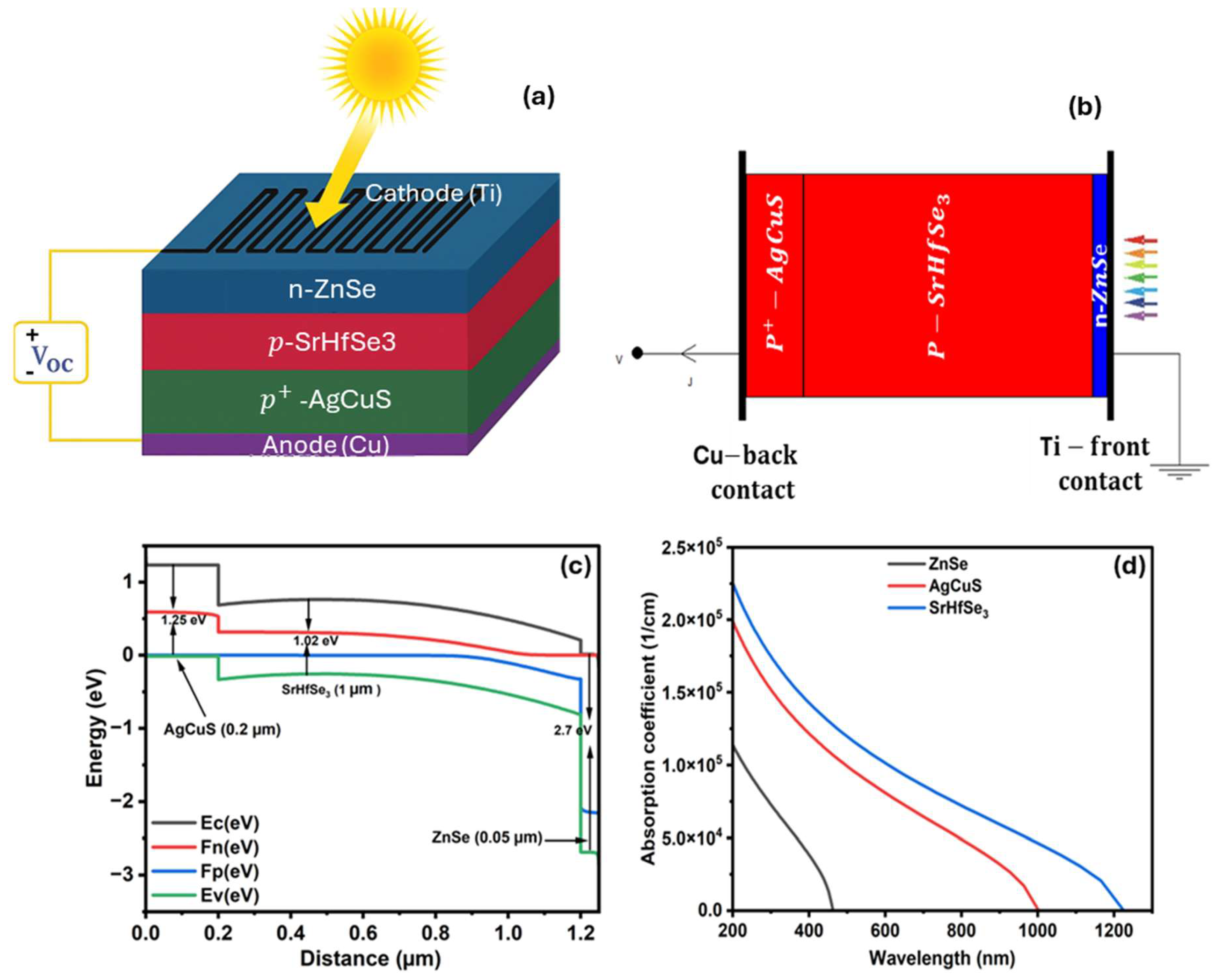
Figure 1. (a) the proposed ZnSe/SrHfSe3/AgCuS photodetector structure; (b) the corresponding device structure as modeled in SCAPS-1D simulations; (c) energy band diagram of the photodetector simulated using SCAPS-1D in which conduction band edge (Ec, black curve) and valence band edge (Ev, green curve), along with the electron quasi-Fermi level (Fn, red curve) and the hole quasi-Fermi level (Fp, blue curve); and (d) the absorption coefficient profiles of ZnSe (black line), AgCuS (red line), and SrHfSe3 (blue line), obtained from SCAPS-1D simulations.
Sci 07 00113 g001
Figure 2. Simulated performance of the photodetector under varying absorber SrHfSe3 layer parameters; (a) J–V curves at different absorber thicknesses (0.4–1.6 μm); (b) the responsivity (red line), and detectivity (blue line) versus absorber thickness at a wavelength of 1100 nm; (c) J–V characteristics with respect to absorber doping levels across range 1 × 10¹⁵–1 × 1020 cm−3; (d) the responsivity (red line), and detectivity (blue line) as a function of absorber doping level at a wavelength of 1100 nm; (e) J–V curves at varying defect densities (1 × 10¹²–1 × 1017 cm−3); and (f) the responsivity (red line), and detectivity (blue line) as function of the defect levels of the absorber at a wavelength of 1100 nm.
Sci 07 00113 g002
Figure 3. Simulated performance of the SrHfSe3-based photodetector with varying window layer ZnSe parameters; (a) J–V curves at different ZnSe thicknesses (0.05–0.25 μm); (b) responsivity and detectivity versus ZnSe thickness at a wavelength of 1100 nm; (c) J–V characteristics for ZnSe doping levels (1 × 10¹⁵–1 × 1020 cm−3); (d) responsivity (red line) and specific detectivity (blue line) as a function of ZnSe doping at a wavelength of 1100 nm; (e) J–V curves at varying defect densities (1 × 10¹²–1 × 1017 cm−3); and (f) Responsivity (red line) and detectivity (blue line) as a function of the defect levels in ZnSe at a wavelength of 1100 nm.
Sci 07 00113 g003
Figure 4. Simulated performance of the SrHfSe3-based photodetector under varying BSF AgCuS layer parameters. (a) J–V curves at different AgCuS thicknesses in a range from 0.05 to 0.3 μm; (b) the responsivity (red line), and detectivity (blue line) versus thickness at a wavelength of 1100 nm; (c) J–V characteristics with respect to the change in AgCuS doping levels (1 × 10¹⁵–1 × 1020 cm−3); (d) the responsivity (red line), and detectivity (blue line) as a function of AgCuS doping at a wavelength of 1100 nm; (e) J–V curves at varying defect densities (1 × 10¹²–1 × 1017 cm−3); and (f) the responsivity (red line), and detectivity (blue line) as function of the defect levels of the AgCuS layer at a wavelength of 1100 nm.
Sci 07 00113 g004
Figure 5. Influence of interfacial defects on photodetector performance at 1100 nm. (a) (J–V) characteristics at the ZnSe/SrHfSe3 interface; (b) the responsivity (red line), and specific detectivity (blue line) versus ZnSe/SrHfSe3 interface defects at a wavelength of 1100 nm; (c) (J–V) characteristics at the SrHfSe3/AgCuS interface; and (d) the responsivity (red line), and specific detectivity (blue line) as a function of SrHfSe3/AgCuS interface defects at a wavelength of 1100 nm.
Sci 07 00113 g005
Figure 6. Impact of working temperature on the photodetector characteristics in the range of 300 K to 500 K at a wavelength of 1100 nm. (a) J–V characteristics; (b) responsivity (red line) and specific detectivity (blue line) as a function of temperature variation at 1100 nm; (c) dark current density versus variation in working temperature; and (d) on/off ratio as a function of working temperature.
Sci 07 00113 g006
Figure 7. The impact of bandgap energy variation in the SrHfSe3 within the range (1.02 eV to 1.15 eV) on the detector performance. (a) Photocurrent density–voltage (J–V) curves versus change in the absorber bandgap; (b) the responsivity (red line), and specific detectivity (blue line) as a function of bandgap energy at a wavelength of 1100 nm; (c) the EQE as a function of bandgap energy; and (d) dark current (red line) and the on/off ratio (blue line) as a function of bandgap energy of absorber layer SrHfSe3.
Sci 07 00113 g007
Figure 8. (a) Simulated current density–voltage (J–V) characteristics of the SrHfSe3-based photodetector under varying illumination intensities from 5 to 100 mW/cm2. (b) The responsivity (red line) and specific detectivity (blue line) as functions of input optical power at a wavelength of 1100 nm.
Sci 07 00113 g008
Figure 9. (a) The Voc (red line) and Jsc (blue line) as a function of the series resistance of the SrHfSe3-based photodetector; (b) the Voc (red line) and Jsc (blue line) versus shunt resistance; (c) the Voc against the electron affinity of SrHfSe3; and (d) the Jsc as a function of the electron affinity of SrHfSe3.
Sci 07 00113 g009
Figure 10. Mott–Schottky (1/C2–V) plots comparing simulated (red line) and fitted (blue line) curves for two key junctions in the device structure. (a) The capacitance–voltage characteristics of the ZnSe/SrHfSe3 heterojunction; (b) the capacitance–voltage for the SrHfSe3/AgCuS junction.
Sci 07 00113 g010
Figure 11. The performance characteristics for the optimized photodetector with (red line) and without (black line) the BSF layer: (a) J–V curves, (b) EQE, (c) spectral responsivity, and (d) spectral detectivity.
Sci 07 00113 g011
Table 1. Summary for Ec (eV) and Ev (eV) for each layer of the device.
Layerχ (eV)Eg (eV)Ec (eV) Ev (eV)
ZnSe4.092.70–4.09– 6.79
SrHfSe33.901.02–3.90–4.92
AgCuS3.901.25–3.35– 4.60
Table 2. Input parameters used for simulation.
StructureZnSe [41]SrHfSe3 [34,40]AgCuS [31]
Thickness (µm)0.0510.2
Bandgap (eV)2.71.021.25
Electron Affinity (eV)4.093.93.350
Dielectric permittivity10.0007.4510.000
Effective DOS at CB (cm−3)1.50 × 10185.60 × 10181.99 × 1019
Effective DOS at VB (cm−3)1.800× 10195.40 × 10181.72 × 1019
Thermal velocity of electron (cm−1)1.00 × 1071.00 × 1071.00 × 107
Thermal velocity of holes
(cm−1)
1.00 × 1071.00 × 1071.00 × 107
Electron mobility (cm2 cm−1s−1)5.00 × 1013.647 ×1011.00 × 102
Hole mobility (cm2 cm−1s−1)6.094 × 1016.094× 1016.60 × 101
Bulk defect density
(cm−3)
1.00 × 10151.00 × 10141.00 × 1015
Shallow uniform acceptor density NA (cm−3)01.00 × 10171.00 × 1019
Shallow uniform doner density Nd (cm−3)1.00 × 101800
Table 3. The work functions and surface recombination velocities for the contacts used in the simulation.
ContactsUnitBack Contact ParametersFront Contact Parameters
Metal work functioneV4.7 [31]3.84 [55]
Surface recombination velocity of holescm/s1.00 × 1071.00 × 107
Surface recombination velocity of holescm/s1.00 × 1071.0 × 107
Table 4. Comparison of photodetector performance for the structure with and without the BSF layer.
Structure Responsivity (A/W)Detectivity (Jones)Wavelength (nm)
ZnSe/SrHfSe30.6751.94 × 10131040
ZnSe/SrHfSe3/
AgCuS
0.852.26 × 10141100
Disclaimer/Publisher’s Note: The statements, opinions and data contained in all publications are solely those of the individual author(s) and contributor(s) and not of MDPI and/or the editor(s). MDPI and/or the editor(s) disclaim responsibility for any injury to people or property resulting from any ideas, methods, instructions or products referred to in the content.