Abstract
To investigate the in situ irradiation effects of gallium nitride at varying temperatures, we combined ion beam-induced luminescence spectroscopy with variable-temperature irradiation using a home-built IBIL system and a GIC4117 2 × 1.7 MV tandem accelerator. Unlike previous static studies—limited to post-irradiation or single-temperature luminescence—we in situ tracked dynamic luminescence changes throughout irradiation, directly capturing the real-time responses of luminescent centers to coupled temperature-dose variations—a rare capability in prior work. To clarify how irradiation and temperature affect the luminescent centers of GaN, we integrated density functional theory (DFT) calculations with literature analysis, then resolved the yellow luminescence band into three emission centers via Gaussian deconvolution: 1.78 eV associated with C/O impurities, 1.94 eV linked to VGa, and 2.2 eV corresponding to CN defects. Using a single-exponential decay model, we further quantified the temperature- and dose-dependent decay rates of these centers under dual-variable temperature and dose conditions. Experimental results show that low-temperature irradiation such as at 100 K suppresses the migration and recombination of VGa/CN point defects, significantly enhancing the radiation tolerance of the 1.94 eV and 2.2 eV emission centers; meanwhile, it reduces non-radiative recombination center density, stabilizing free excitons and donor-bound excitons, thereby improving near-band-edge emission center resistance. Notably, the 1.94 eV emission center linked to gallium vacancies exhibits superior cryogenic radiation tolerance due to slower defect migration and more stable free exciton/donor-bound exciton states. Collectively, these findings reveal a synergistic regulation mechanism of temperature and radiation fluence on defect stability, addressing a key gap in static studies, providing a basis for understanding degradation mechanisms of gallium nitride-based devices under actual operating conditions (coexisting temperature fluctuations and continuous radiation), and offering theoretical/experimental support for optimizing radiation-hardened gallium nitride devices for extreme environments such as space or nuclear applications.
1. Introduction
Gallium nitride (GaN), as a core material of third-generation semiconductors, occupies an irreplaceable position in optoelectronic devices [1] and high-frequency electronic devices [2]. Its exceptional high power density and high-frequency response characteristics make GaN-based high-electron-mobility transistors (HEMTs) an ideal alternative to traditional silicon-based devices [3]. Furthermore, GaN crystals are renowned for their radiation damage resistance [4], an advantage rooted in their wide-bandgap properties and the buffering effect of high intrinsic defect concentration on radiation-induced damage. This renders them indispensable key materials in radiation-resistant scenarios such as satellite systems and nuclear applications [5,6].
However, in practical aerospace applications, GaN materials and devices are often subjected to long-term exposure to the synergistic effects of complex radiation environments (protons, X-rays, β-rays, γ-rays, neutrons) and temperature fluctuations [7]. These extreme conditions induce the formation, migration, and annihilation of internal defects (e.g., vacancies, interstitial atoms, and dislocations) within the material, resulting in changes to its microstructure. Such microstructural changes further manifest as fluctuations in optical properties, including luminous efficiency and a shift in peak wavelength. Characterizing the dynamic changes in optical properties can effectively elucidate the evolution of defects; meanwhile, conducting ground-based temperature and radiation effect testing is critical for ensuring the stability of aerospace components, playing a significant role in revealing the failure mechanisms of GaN materials in space environments and ensuring the long-term stability of spaceborne devices. Traditional optical characterization techniques (e.g., photoluminescence (PL) and cathodoluminescence (CL)) can analyze the structural changes of defects before and after irradiation but have inherent limitations in revealing the dynamic evolution of defects. First, these methods only capture static defect information at discrete time points (before and after irradiation) and fail to dynamically track the generation, migration, and recombination behaviors of defects during the irradiation process. Second, limited by the accumulated damage in samples under strong radiation or high temperatures, the test results struggle to accurately reflect the true evolution of defects.
In studies on the radiative spectroscopy characterization of GaN, researchers have conducted comprehensive and in-depth analyses of the luminescence centers corresponding to its core features—namely, band-edge transitions and the yellow luminescence band (YLB). Early investigations attributed YLB to radiative recombination between shallow donor defects and deep acceptor defects [8,9,10,11,12,13,14,15,16], whereas subsequent work has progressively focused on the microscopic identification of specific point defects. Among these, carbon substitutional defects at nitrogen sites (CN) have been widely confirmed as the primary luminescence center responsible for YLB. For instance, experiments by Reshchikov’s team on GaN grown via the a mmonothermal method demonstrated that CN acceptor defects dominate YLB emission [16]. Theoretical calculations further support this conclusion: Lyons et al., [17] using hybrid functional calculations, revealed that CN is not a shallow acceptor as traditionally assumed but a deep-level acceptor with an ionization energy of approximately 0.90 eV. Its optical emission peak at 2.14 eV directly corresponds to the yellow light region. Dai’s team further confirmed through carbon implantation experiments that carbon doping significantly modulates YLB intensity, highlighting the critical role of carbon-related defects [18]. Beyond CN, gallium vacancies (VGa) have also been proposed as a potential luminescence center for YLB, though their contribution is generally secondary. J. L. Lyons et al. [19] noted that VGa exhibits a higher formation energy in n-type GaN, whereas CN is more stable across a broad range of Fermi levels. VGa may indirectly contribute to YLB through complexes, but formation energy calculations indicate it exists at lower concentrations in isolated states. Notably, growth methods and doping conditions dominance in HVPE/MOCVD-grown GaN [16] directly influence the temperature dependence of YLB emission and hole capture mechanisms in n-type GaN [19]. These findings indicate the micro-origin of YLB is intrinsically linked to defect types and growth processes, necessitating high-sensitivity characterization techniques to elucidate dynamic behaviors.
To address these challenges, this study innovatively employs temperature-variable ion beam-induced luminescence (IBIL) technology. This approach overcomes limitations of traditional techniques in studying temperature-dependent defect evolution. Leveraging the high sensitivity and dynamic response capabilities of luminescence-based characterization, IBIL captures optical signals during radiative recombination processes, enabling real-time micro-property evolution. The spectral features directly correlate with the physical mechanisms governing radiative recombination.
In addition, IBIL technology utilizes high-energy ion beams to excite materials, depositing energy in a highly localized manner. This leads to excitation densities orders of magnitude higher than those achieved by other methods. In contrast, conventional methods such as lasers or X-rays cannot reach such high densities due to their broader energy dispersion and lower stopping power. Consequently, ion irradiation through IBIL can be emerged as an irreplaceable tool for simulating high-energy-density non-equilibrium processes under extreme conditions, particularly for radiation damage studies relevant to nuclear reactor environments and space applications.
This technique systematically investigates bulk single-crystal GaN through variable-temperature measurements, quantifying the differential effects of temperature and proton fluence (energy: 2 MeV, fluence: 1013–1015 ion/cm2) on defects across a 100–300 K temperature range, thereby providing critical parameters for optimizing radiation-hardened designs under varying temperature conditions. It effectively separates the luminescence contributions from different defects, offering key experimental evidence for elucidating the origin of the yellow luminescence band (YLB) in GaN. By not only establishing a new method for analyzing the dynamic evolution of GaN defects under variable-temperature conditions but also paving the way for investigating the origins of complex luminescence mechanisms such as YLB through its spectral-temperature decoupling capability, IBIL critically reveals the radiation damage mechanisms of GaN in extreme environments (e.g., nuclear reactors and deep-space detectors). These findings provide critical theoretical guidance and material optimization strategies for the reliable application of GaN in high-radiation scenarios.
2. Experiments and Simulations
The IBIL analysis system was installed on the GIC4117 2 × 1.7 MV tandem accelerator at Beijing Normal University. During IBIL measurements, emitted photons were transmitted via optical fiber to an Ocean Optics QE-Pro spectrometer for reception. Spectral data acquisition and storage were performed using the OceanView software V1.1, with an integration time of 0.5 s. A backscatter system was integrated into the IBIL target chamber to monitor beam fluctuations. The sample stage, provided by Instec Inc. (Boulder, CO, USA), enables vacuum-compatible temperature control ranging from 80 K to 900 K, with a stability of ±1 K. The In situ IBIL system enabled real-time monitoring of luminescence spectra, yielding in situ spectral data under ambient conditions. Comparative analysis of IBIL spectra acquired at different temperatures further elucidated the temperature-dependent luminescence behavior of GaN. All IBIL luminescence measurements were conducted in a high-vacuum chamber with a pressure of approximately 9 × 10⁻⁴ Pa.
The bulk single-crystal GaN samples used in this study were grown with HVPE and supplied by Suzhou Navitech Co., Ltd, Suzhou, China. The as-grown crystals exhibited a thickness of 400 ± 30 μm, a room-temperature resistivity (R) ≤ 0.02 Ω·cm, and a dislocation density (ρ) < 3 × 106 cm−2.
IBIL measurements were conducted under variable temperature conditions (100–300 K). A 2 MeV H+ ion beam with a diameter of 6.7 mm was employed, and spectral data were acquired at 0.5 s intervals, with the beam current of 16 nA.
For computational simulations, this study employs SRIM (The Stopping and Range of Ions in Matter) Monte Carlo simulations and first-principles calculations. SRIM is a program that models ion-matter interactions via Monte Carlo methods, providing critical insights into ion energy loss, depth distribution, and target material damage [20]. In this work, H+ ion implantation into GaN was simulated using SRIM with 90,000 incident particles. The simulation parameters were configured as follows: GaN density = 6.1 g/cm3, H+ energy = 2 MeV, and incident angle = perpendicular to the GaN surface (consistent with IBIL experimental settings). The simulated energy loss profiles for H+ in GaN under electronic stopping (Se) and nuclear stopping (Sn) regimes are shown in Figure 1. Among these, electronic stopping dominated energy dissipation, accounting for 99.86% of the total energy loss. The peak energy loss positions were observed at 23.8 μm (Se) and 24.5 μm (Sn), with a maximum projected ion range of 26.6 μm.

Figure 1.
The SRIM simulation results of 2 MeV H+ incident GaN are the ionization and nuclear blocking energy deposition distribution of H+ in GaN.
First-principles calculations, a core computational approach in materials science that relies exclusively on seven fundamental physical constants, enable the accurate prediction of the intrinsic ground-state properties of the material (e.g., electronic structure, defect formation energy) through solving the Schrödinger equation without introducing empirical parameters. In studies of the YLB emission mechanism in GaN, VGa and CN are widely recognized as the most controversial sources of deep acceptor defects [10,11,12]. VGa refers to an intrinsic point defect formed by the absence of Ga atoms, and CN (carbon acceptor on nitrogen site) refers to a compensatory acceptor defect formed by C atoms substituting for N atoms at lattice sites. Recent systematic investigations have thoroughly elucidated the microscopic mechanisms of CN defects, with key insights from defect energy level characterization. Notably, work by J. Lyons on carbon-related defects challenges the currently accepted view that C substituting for N (i.e., CN) is a shallow acceptor; instead, Lyons’ study found that CN has an ionization energy of 0.90 eV [17]. This ionization energy aligns with subsequent systematic studies, which confirm that the CN-dominated YL1 band peaks at 2.17 eV—originating from electron transitions from shallow donor levels (at temperatures below 50 K) or the conduction band (at elevated temperatures) to the −/0 energy level of CN, which lies approximately 0.916 ± 0.003 eV above the valence band maximum (VBM) of GaN. As an acceptor defect, CN thus introduces an acceptor level roughly 0.9 eV above the VBM; through the p-orbitals of carbon atoms, it dominates the downward shift of the Fermi level, significantly enhancing the hole concentration in the valence band and rendering CN an effective dopant source for p-type GaN [16,21].
Given the well-established understanding of the luminescence mechanisms and thermoelectric behavior of CN, this study shifts its focus to analyzing the formation energy of VGa defects in wurtzite GaN to complement the atomic-scale characterization of the controversial defects involved in YLB origin. Leveraging density functional theory (DFT) combined with the GGA + U method—with pseudopotentials set as on-the-fly generated (OTFG) ultrasoft pseudopotentials, a plane-wave cutoff energy of 570 eV, k-point sampling set to “Fine”, and spin-polarized calculations performed—with Ueff (Ga-3d) = 0.3 eV and Ueff (N-2p) = 4.79 eV to correct self-interaction errors and bandgap deviations—the lattice constants of GaN are defined as a = b = 3.19 Å, c = 5.19 Å, with α = β = 90° and γ = 120°, belonging to the P63mc(186) space group. Based on these parameters, a primitive cell of wurtzite GaN was first constructed. We systematically investigate the formation energies and electronic structural properties of VGa defects under various charge states. By constructing a 4 × 4 × 1 supercell model (containing 128 atoms) to minimize defect-defect interactions, under these settings, the band structures of VGa defects in various charge states (q) were computed. The formation energy for a defect with charge state q is defined as:
The formula represents the formation energy of a VGa defect in charge state q. Here, denotes the number of atoms added ( > 0) or removed ( < 0) relative to the defect-free system, and corresponds to the chemical potential of the relevant atom. is the Fermi energy, represents the valence band maximum energy, is the valence band top correction between the defective and defect-free systems, and denotes the correction energy of the computed system.
Using the parameters = −77,549.6 eV and = −75,397.22 eV, the chemical potential μi of Ga is −2145.62 eV, and = −2148.5 eV under N-rich conditions; the calculated results are summarized in Table 1. The simulation results show that the luminescent transitions of VGa defects at ε(0/−2) = 1.38 eV and ε(−2/−3) = 1.56 eV lie within the bandgap, making them deep acceptor defect energy levels that may contribute to the yellow luminescence band.

Table 1.
The formation energies of VGa defects in various charge states calculated using first-principles methods.
3. Experimental Results and Discussion
To investigate H+ ion-induced luminescence in GaN across varying temperatures, this study employed ion beam-induced luminescence (IBIL) spectroscopy on bulk single-crystal GaN samples. Measurements were conducted using a 2 MeV H+ ion beam under both room temperature and controlled conditions ranging from 100 to 300 K. Comparative analysis of the resulting spectra revealed temperature-dependent luminescence behavior in GaN.
3.1. In Situ IBIL Experiments Under Room-Temperature H+ Irradiation
In this study, the IBIL spectra of GaN under varying ion fluences were acquired using an IBIL analysis system. As shown in Figure 2, the IBIL spectra of GaN at room temperature exhibit two distinct emission bands: a broad visible luminescence band and a narrower ultraviolet (UV) emission band. To resolve the detailed characteristics of the YLB and near-band-edge (NBE) peaks, the spectra were converted into energy-dispersive distributions and subjected to Gaussian-based peak deconvolution. Given the widely accepted assumption that interband transitions follow Gaussian distributions, Gaussian peak fitting was employed to analyze the spectral data. Combined with first-principles calculations and prior investigations into the origin of YLB emissions in GaN [16,22,23,24], three distinct luminescence centers were identified through Gaussian deconvolution: a 1.78 eV emission center attributed to C/O impurities, a 1.94 eV emission center linked to VGa defects, and a 2.2 eV emission center associated with CN defects, as illustrated in Figure 3b. For the NBE region, the spectrum was decomposed into two sharp peaks corresponding to FE (3.32 eV) and D0X (3.24 eV) emissions, as illustrated in Figure 3a.
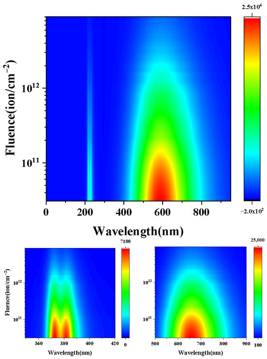
Figure 2.
Evolution of emission intensity with ion fluence for bulk single-crystal GaN under room-temperature 2 MeV H+ irradiation.
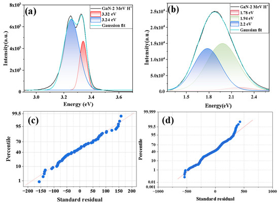
Figure 3.
Gaussian splitting peaks of bulk single-crystal GaN (a) Gaussian peaks near the band edge at room temperature (b) Gaussian splitting peaks in the yellow light band. (c,d) are the standard residual plots after Gaussian peak fitting of (a,b).
Figure 4 and Figure 5 depict the evolution of emission center intensities for the YLB and NBE regions, respectively, as functions of H+ ion fluence. Both spectra exhibit an initial rapid decline in intensity followed by a gradual stabilization. This trend arises from cumulative ion irradiation effects: as H+ ion fluence increases, point defects proliferate and aggregate into larger defect clusters, which act as non-radiative recombination centers, suppressing luminescence efficiency. Concurrently, lattice damage disrupts the crystal structure, hindering exciton diffusion and migration while reducing exciton capture probabilities due to bond stress relaxation. Additionally, localized temperature spikes along the ion trajectory, attributed to thermal spike effects, elevate lattice temperatures, accelerating exciton dissociation and increasing non-radiative recombination via lattice vibrations. These combined mechanisms result in a continuous reduction in emission yield during the early stages of ion implantation [25].
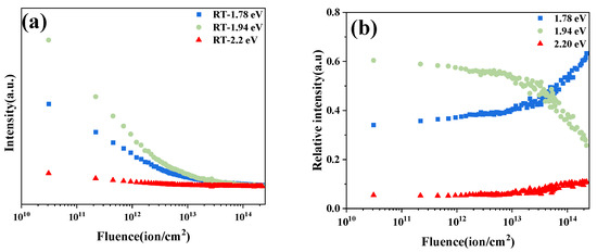
Figure 4.
(a) Evolution characteristics of the emission center intensity in the yellow luminescence band (YLB) region with H+ ion fluence, depicting the main changes in this spectral region after irradiation. (b) The relative intensity of the peak luminescence centers within the YLB with the accumulation of ion flux. Note: ‘Relative intensity’ is obtained via maximum normalization (using Origin software).
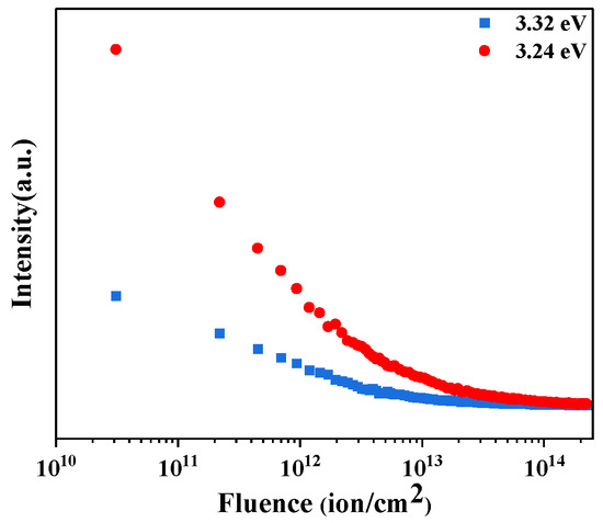
Figure 5.
Evolution of NBE emission center intensity with H+ ion fluence.
The evolution of relative intensities of distinct luminescence centers in the yellow YLB, as shown in Figure 4a, reveals the following trends with increasing H+ fluence: the relative intensity of the 1.78 eV emission center (associated with C/O impurities) progressively increases, while the 1.94 eV emission center (linked to VGa defects) exhibits a continuous decrease. The 2.2 eV emission center (attributed to CN defects) also shows enhanced intensity but remains at a relatively low level throughout the irradiation process. These findings are consistent with the experimental observations by Reshchikov et al., who reported that CN defects exhibit superior luminescence stability under irradiation and are less prone to forming non-radiative recombination centers compared to other defect types [26]. Further analysis of NBE emission behavior (Figure 5) indicates that the D0X emission intensity declines more rapidly than the FE emission center during the initial stages of H+ irradiation, suggesting weaker radiation resistance of D0X. This disparity arises from the dual dependence of D0X intensity on both exciton concentration and donor-type defect states. The H+ implantation process simultaneously suppresses exciton diffusion and alters the population dynamics of point defects, leading to a significant reduction in the probability of exciton capture by donor centers. Consequently, the accelerated decay of D0X emission underscores the hierarchical susceptibility of defect-mediated luminescence channels to ion irradiation, where FE emissions rely solely on intrinsic exciton behavior, whereas D0X emissions are more vulnerable to ion-induced structural modifications and defect engineering.
To systematically investigate the decay dynamics of distinct luminescence centers, a single-exponential decay fitting model was applied to analyze the temporal evolution of GaN luminescence [27]. The decay behavior was described by the following equation:
where I denotes the luminescence intensity dependent on H+ ion irradiation fluence, F denotes the incident ion flux, and a, b, and f are fitting parameters. The parameter f characterizes the decay rate, where larger f values correspond to better stability and higher radiation resistance, and an increase in f value indicates enhanced stability of the material against ion-induced degradation [28].
The decay rates (f) of distinct luminescence centers, determined through single-exponential decay fitting analysis, are summarized in Table 2.
Table 2.
The attenuation rate f of different luminescence centers with ion flux fits value at room temperature.
The fitted decay rate (f) aligns with the luminescence behavior observed in Figure 4 and Figure 5. Specifically, the VGa defect, characterized by its high migration rate and poor radiation resistance, exhibits accelerated decay due to its susceptibility to ion-induced damage or quenching under irradiation [29]. This experimental observation corresponds to the smallest f value among all defect centers, confirming its dominant role in the observed rapid luminescence degradation.
3.2. In Situ Irradiation Luminescence (IBIL) Experiments Under 100–300 K H+ Irradiation
Figure 6 presents the in situ IBIL spectra of GaN under variable-temperature conditions, capturing the real-time intensity evolution during irradiation.
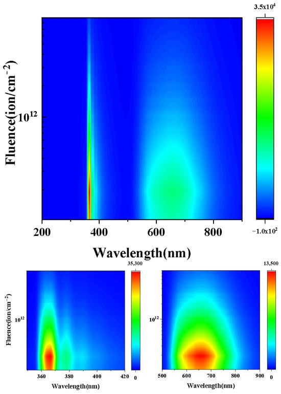
Figure 6.
Variation in luminous intensity of H+ irradiated monocrystalline GaN with 2 MeV (100–300 K) at variable temperature (temperature was gradually increased from 100 K to 300 K via a temperature-controlled chamber).
To elucidate the physical mechanisms and temperature-dependent behavior of NBE luminescence in GaN under cryogenic conditions, this study employed in situ IBIL spectroscopy combined with Gaussian peak deconvolution. As shown in Figure 7, At a low temperature of 100 K, the proton-induced spectra exhibit sharp NBE emission peaks dominated by free excitons (FE: 361.65 nm/3.43 eV) and donor-bound excitons (D0X: 366.92 nm/3.38 eV), accompanied by distinct phonon-assisted sideband structures on both sides with an energy separation of 89 meV (consistent with the energy of longitudinal optical (LO) phonons in GaN [30], the energy of the optical phonon branch in bulk GaN reported in Ref. [30] is 60–90 meV), as illustrated in Figure 8. When the temperature is elevated to room temperature, these phonon sidebands are suppressed due to thermal activation, leaving only the broadened intrinsic contributions of FE and D0X—an observation consistent with the NBE features measured by ambient-temperature IBIL. Comparative analysis of peak positions further reveals that the low-temperature NBE transition energies (3.43–3.38 eV) lie closer to the intrinsic bandgap than their room-temperature counterparts (3.32–3.24 eV). This phenomenon is attributed to the suppression of thermal broadening effects and the enhancement of exciton binding energy at cryogenic temperatures, which effectively inhibit non-radiative phonon interactions and stabilize the excitonic states.
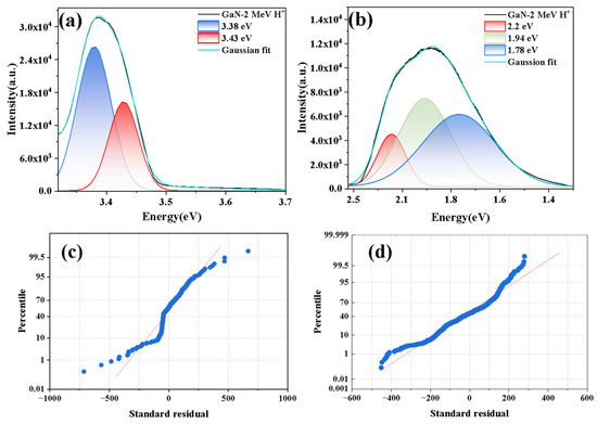
Figure 7.
Gaussian splitting peak of massive single crystal GaN at variable temperature (at 100 K). (a) Gaussian peaks near the band edge (b) Gaussian splitting peaks in the yellow light band. (c,d) are the standard residual plots after Gaussian peak fitting of (a,b).
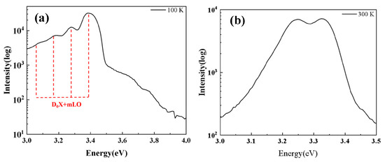
Figure 8.
Temperature-Dependent IBIL Spectra of GaN in the Near-Band-Edge Region (a) 100 K 2 MeV H+; (b) 300 K 2 MeV H+.
To elucidate the dynamic evolution mechanisms of luminescent centers in the YLB under coupled temperature and H+ fluence conditions, this study employed in situ IBIL spectroscopy combined with a single-exponential decay model (Equation (2)) to systematically analyze intensity variations and H⁺ fluence-dependent relative intensity trends across distinct YLB emissive centers, including FE, D0X, and VGa-related defects. As shown in Figure 9 and Figure 10, the experimental results reveal that the relative intensity of the 1.94 eV emission band associated with VGa defects exhibits a significantly slower decay rate under variable-temperature conditions compared to room-temperature measurements (Figure 4b vs. Figure 9b). This phenomenon is attributed to the reduced migration rate of VGa defects at cryogenic temperatures, which suppresses defect recombination dynamics and stabilizes their concentration [15]. By applying the single-exponential decay model (Equation (2)) to the variable-temperature spectra, the derived decay rate constants for all emissive centers were quantified and compared with their room-temperature counterparts in Table 3.
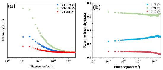
Figure 9.
Evolution of different luminescence centers of bulk single crystal GaN with ion flux under temperature variation: (a) Evolution of different luminescence center intensities with ion flux in GaN yellow band; (b) The relative intensities of different luminescence centers in the GaN yellow band change with ion flux.
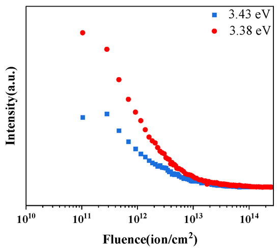
Figure 10.
The variation in the intensity of different luminescence centers at the near-band edge of GaN with ion flux.
Table 3.
The attenuation rate f of different luminescence centers with ion flux fits value.
The single-exponential decay model (Equation (2)) was applied to the variable-temperature spectra to quantify the decay rate constants of all emissive centers. As summarized in Table 3, the decay rates (k) of the 1.78 eV, 1.94 eV, and 2.2 eV luminescent centers in the YLB increased under variable-temperature conditions (100–300 K) compared to room temperature. This enhancement indicates improved radiation resistance of YLB emissive centers at elevated temperatures. The strengthened radiation tolerance is attributed to reduced migration rates of C/O-related composite defects, VGa defects, and CN defects at low temperatures, which suppress the formation of complex non-radiative recombination centers, thereby preserving material luminescence properties. Specifically, the radiation resistance of the 1.78 eV, 1.94 eV, and 2.2 eV centers increased by 17%, 5.0-fold, and 20.8%, respectively, under variable-temperature conditions. Under both ambient and variable-temperature (100–300 K) conditions, the FE peak exhibited superior radiation resistance compared to the D0X peak in the NBE region. This difference arises because FE, with its higher binding energy, demonstrates greater resilience to irradiation and thermal excitation, whereas D0X is more susceptible to dissociation or non-radiative recombination under such conditions [31].
4. Conclusions
This study employed in situ IBIL spectroscopy to systematically investigate the dynamic evolution mechanisms of luminescence centers in GaN under coupled proton irradiation and temperature effects. By combining first-principles calculations with Gaussian decomposition of proton-excited spectra, three distinct emission sources in the YLB were identified: a 1.78 eV emission center (associated with C/O impurities), a 1.94 eV emission center (arising from electron transitions from the conduction band to the VGa defect ε(0/−2) energy level), and a 2.2 eV emission center (linked to CN defect excitation). A single exponential decay model was applied to analyze the temporal evolution of these luminescence centers, revealing the significant influence of temperature regulation on their radiation tolerance. Experimental results demonstrate that under low-temperature (100 K) irradiation, the radiation resistance of the VGa defect (1.94 eV) increased by 5-fold, significantly surpassing the 20.8% enhancement observed for the CN-related 2.2 eV center. This discrepancy arises from the suppression of defect migration/recombination processes at low temperatures. Additionally, low-temperature conditions reduced non-radiative recombination center density and enhanced the stability of FE and D0X. Notably, FE exhibited superior radiation tolerance in low-temperature environments due to its higher binding energy. Compared to conventional ex situ characterization methods, in situ IBIL spectroscopy enabled real-time monitoring of luminescence behavior during irradiation, quantifying the temperature-irradiation coupling effects on the radiation resistance of GaN. These findings provide theoretical support for GaN material applications in extreme radiation environments and establish a foundational basis for optimizing radiation-hardened GaN-based device design.
Supplementary Materials
The following supporting information can be downloaded at: https://www.mdpi.com/article/10.3390/qubs10010002/s1.
Author Contributions
X.P.: Undertook the drafting of the manuscript and performed data processing. W.J.: Primarily executed the experimental procedures and collected the experimental data. R.C.: Assisted in the implementation of experiments and conducted supplementary literature investigations. H.H.: Participated in background literature research and contributed to the revision and polishing of the manuscript. S.L.: Contributed to the revision and polishing of the manuscript. Corresponding authors X.O. and M.Q.: Proposed the core research questions, designed the overall study framework, and provided critical guidance for optimizing experimental execution. All authors have read and agreed to the published version of the manuscript.
Funding
This research was supported by National Natural Science Foundation of China (No.12205016), Young Elite Scientists Sponsorship Program by CAST (No.2023QNRC001) and the fund of innovation center of radiation application (No. KFZC2021020801).
Data Availability Statement
The original contributions presented in this study are included in the article/Supplementary Materials. Further inquiries can be directed to the corresponding authors.
Conflicts of Interest
The authors declare no conflict of interest.
References
- Sharma, R.C.; Nandal, R.; Tanwar, N.; Yadav, R.; Bhardwaj, J.; Verma, A. Gallium arsenide and gallium nitride semiconductors for power and optoelectronics devices applications. J. Phys. Conf. Ser. 2023, 2426, 012008. [Google Scholar] [CrossRef]
- Musumeci, S.; Vincenzo, B. Gallium nitride power devices in power electronics applications: State of art and perspectives. Energies 2023, 16, 3894. [Google Scholar] [CrossRef]
- Sharma, N.; Raman, A.; Ranjan, R. GaN-Based High Electron Mobility Transistor. In Semiconductor Nanoscale Devices: Materials and Design Challenges; Bentham Science Publishers: Sharjah, United Arab Emirates, 2025; pp. 193–212. [Google Scholar]
- Polyakov, A.Y.; Pearton, S.J.; Frenzer, P.; Ren, F.; Liu, L.; Kim, J. Radiation effects in GaN materials and devices. J. Mater. Chem. C 2013, 1, 877–887. [Google Scholar] [CrossRef]
- Sequeira, M.C.; Mattei, J.G.; Vazquez, H.; Djurabekova, F.; Nordlund, K.; Monnet, I.; Mota-Santiago, P.; Kluth, P.; Grygiel, C.; Zhang, S.; et al. Unravelling the secrets of the resistance of GaN to strongly ionising radiation. Commun. Phys. 2021, 4, 51. [Google Scholar] [CrossRef]
- Wang, J.; Mulligan, P.; Brillson, L.; Cao, L.R. Review of using gallium nitride for ionizing radiation detection. Appl. Phys. Rev. 2015, 2, 031102. [Google Scholar] [CrossRef]
- Ji, Q.; Yang, M.; Cheng, Q.; Liu, J.; Liu, S. Study on proton irradiation effect of GaN optical and electrical properties. J. Korean Phys. Soc. 2023, 83, 372–380. [Google Scholar] [CrossRef]
- Pankove, J.; Hutchby, J. Photoluminescence of ion-implanted GaN. J. Appl. Phys. 1976, 47, 5387–5390. [Google Scholar] [CrossRef]
- Glaser, E.R.; Kennedy, T.A.; Doverspike, K.; Rowland, L.B.; Gaskill, D.K.; Freitas, J.A., Jr.; Asif Khan, M.; Olson, D.T.; Kuznia, J.N.; Wickenden, D.K. Optically detected magnetic resonance of GaN films grown by organometallic chemical-vapor deposition. Phys. Rev. B 1995, 51, 13326. [Google Scholar] [CrossRef]
- Tung, L.T.; Lin, K.; Chang, E.; Huang, W.C.; Hsiao, Y.L.; Chiang, C.H. Photoluminescence and Raman studies of GaN films grown by MOCVD. J. Phys. Conf. Ser. 2009, 187, 012021. [Google Scholar] [CrossRef]
- Yi, G.; Wessels, B. Compensation of n-type GaN. Appl. Phys. Lett. 1996, 69, 3028–3030. [Google Scholar] [CrossRef]
- Zhang, X.; Kung, P.; Saxler, A.; Walker, D.; Wang, Τ.; Razeghi, M. Photoluminescence Study of GaN. Acta Phys. Pol. A 1995, 88, 601–606. [Google Scholar] [CrossRef]
- Hofmann, D.; Kovalev, D.; Steude, G.; Meyer, B.K.; Hoffmann, A.; Eckey, L.; Heitz, R.; Detchprom, T.; Amano, H.; Akasaki, I. Properties of the Yellow luminescence in undoped GaN epitaxial layers. Phys. Rev. B 1995, 52, 16702. [Google Scholar] [CrossRef]
- Chen, H.M.; Chen, Y.G.; Lee, M.C.; Feng, M.S. Yellow luminescence in n-type GaN epitaxial films. Phys. Rev. B 1997, 56, 6942. [Google Scholar] [CrossRef]
- Reshchikov, M.A.; Hadis, M. Luminescence properties of defects in GaN. J. Appl. Phys. 2005, 97, 5–19. [Google Scholar] [CrossRef]
- Reshchikov, M.A. On the Origin of the Yellow Luminescence Band in GaN. Phys. Status Solidi (b) 2023, 260, 2200488. [Google Scholar] [CrossRef]
- Lyons, J.L.; Janotti, A.; de Walle, C.G.V. Carbon impurities and the yellow luminescence in GaN. Appl. Phys. Lett. 2010, 97, 152108. [Google Scholar] [CrossRef]
- Dai, L.; Ran, G.; Zhang, J.; Duan, X.F.; Lian, W.C.; Qin, G.G. C and Si ion implantation and the origins of yellow luminescence in GaN. Appl. Phys. A 2004, 79, 139–142. [Google Scholar] [CrossRef]
- Reshchikov, M.A.; Korotkov, R.Y. Analysis of the temperature and excitation intensity dependencies of photoluminescence in undoped GaN films. Phys. Rev. B 2001, 64, 115205. [Google Scholar] [CrossRef]
- Ziegler, J.F.; Ziegler, M.D.; Biersack, J.P. SRIM—The stopping and range of ions in matter (2010). Nucl. Instrum. Methods Phys. Res. Sect. B-Beam Interact. Mater. At. 2010, 268, 1818–1823. [Google Scholar] [CrossRef]
- Ji, H.; Song, C.; Liao, H.; Yang, N.; Wang, R.; Tang, G.; Cao, W. Theoretical investigation of electronic structure and thermoelectric properties of CN point defects in GaN. J. Alloys Compd. 2023, 969, 172398. [Google Scholar] [CrossRef]
- Armitage, R.; Hong, W.; Yang, Q.; Feick, H.; Gebauer, J.; Weber, E.R.; Hautakangas, S.; Saarinen, K. Contributions from gallium vacancies and carbon-related defects to the “yellow luminescence” in GaN. Appl. Phys. Lett. 2003, 82, 3457–3459. [Google Scholar] [CrossRef]
- Wang, L.; Richter, E.; Weyers, M. Red luminescence from freestanding GaN grown on LiAlO2 substrate by hydride vapor phase epitaxy. Phys. Status Solidi (a) 2007, 204, 846–849. [Google Scholar] [CrossRef]
- Reshchikov, M.A.; Usikov, A.; Helava, H.; Makarov, Y. Fine structure of the red luminescence band in undoped GaN. Appl. Phys. Lett. 2014, 104, 032103. [Google Scholar] [CrossRef]
- Jiménez-Rey, D.; Peña-Rodríguez, O.; Manzano-Santamaría, J.; Olivares, J.; Muñoz-Martín, A.; Rivera, A.; Agulló-López, F. Ionoluminescence induced by swift heavy ions in silica and quartz: A comparative analysis. Nucl. Instrum. Methods Phys. Res. Sect. B Beam Interact. Mater. At. 2012, 286, 282–286. [Google Scholar] [CrossRef]
- Reshchikov, M.A. Photoluminescence from defects in GaN. Gallium Nitride Materials and Devices XVIII. SPIE 2023, 12421, 58–72. [Google Scholar]
- Qiu, M.L.; Yin, P.; Wang, G.F.; Song, J.G.; Luo, C.W.; Wang, T.S.; Zhao, G.Q.; Lv, S.S.; Zhang, F.S.; Liao, B. In situ luminescence measurement of 6H-SiC at low temperature. Chin. Phys. B 2020, 29, 046106. [Google Scholar] [CrossRef]
- Zheng, L.; Wang, G.F.; Qiu, M.L.; Chu, Y.J.; Xu, M.; Yin, P. Ionoluminescence spectra of a ZnO single crystal irradiated with 2.5 MeV H+ ions. Chin. Phys. Lett. 2017, 34, 087801. [Google Scholar] [CrossRef]
- Sedhain, A.; Li, J.; Lin, J.Y.; Jiang, H.X. Nature of deep center emissions in GaN. Appl. Phys. Lett. 2010, 96, 151902. [Google Scholar] [CrossRef]
- Zhang, Z.; Wang, T.; Jiang, H.; Xu, X.; Wang, J.; Wang, Z.; Liu, F.; Zhang, Y.; Wang, P.; Gao, P.; et al. Phonon dispersion of buckled two-dimensional GaN. Nat. Commun. 2024, 15, 10436. [Google Scholar] [CrossRef]
- Bunea, G.E.; Herzog, W.D.; Ünlü, M.S.; Goldberg, B.B.; Molnar, R.J. Time-resolved photoluminescence studies of free and donor-bound exciton in GaN grown by hydride vapor phase epitaxy. Appl. Phys. Lett. 1999, 75, 838–840. [Google Scholar] [CrossRef]


Disclaimer/Publisher’s Note: The statements, opinions and data contained in all publications are solely those of the individual author(s) and contributor(s) and not of MDPI and/or the editor(s). MDPI and/or the editor(s) disclaim responsibility for any injury to people or property resulting from any ideas, methods, instructions or products referred to in the content. |
© 2026 by the authors. Licensee MDPI, Basel, Switzerland. This article is an open access article distributed under the terms and conditions of the Creative Commons Attribution (CC BY) license.