Article

Automated Solar PV Simulation System Supported by DC–DC Power Converters

1
Electrical Engineering Energy and Automation Department (DEEEA), Instituto Superior de Engenharia de Lisboa (ISEL), Instituto Politécnico de Lisboa (IPL), Estrada de Benfica 529, 1549-020 Lisboa, Portugal
2
Instituto de Engenharia de Sistemas e Computadores: Investigação e Desenvolvimento em Lisboa (INESC-ID Lisbon), 1000-029 Lisboa, Portugal
3
Low Carbon Energy Conversion (LCEC), Rua Conselheiro Emídio Navarro 1, 1959-007 Lisboa, Portugal
4
Sustainable Research and Development Center (SustainRD), ESTSetubal, Polytechnic Institute of Setúbal, 2914-508 Setúbal, Portugal
5
Centre of Technology and Systems (CTS), Instituto de Desenvolvimento de Novas Tecnologias (UNINONA), Electrical Engineering Department (DEE), Faculdade de Ciências e Tecnologia (FCT), Universidade Nova de Lisboa (UNL), 2829-516 Caparica, Portugal
*
Author to whom correspondence should be addressed.
Designs 2023, 7(2), 36; https://doi.org/10.3390/designs7020036
Submission received: 11 January 2023 / Revised: 11 February 2023 / Accepted: 21 February 2023 / Published: 1 March 2023
(This article belongs to the Topic Power Electronics Converters)

Abstract

:
Solar photovoltaic simulators are valuable tools for the design and evaluation of several components of photovoltaic systems. They can also be used for several purposes, such as educational objectives regarding operation principles, control strategies, efficiency, maintenance, and other aspects. This paper presents an automated solar photovoltaic simulation system with the capability to generate automated tests considering different parameters of solar photovoltaic panels and different operation conditions. The proposed simulator is composed of three buck-boost DC–DC power converters controlled in such a way that will behave similarly to solar photovoltaic panels. It allows to introduce additional variable loads and maximum power point tracker algorithms similar to real systems. Some converters are controlled by a DSP microcontroller connected to a single programmable logic controller which generates the automated tests. Thus, using the presented solution, it is possible to implement the I-V and P-V characteristic curves of solar photovoltaic panels and evaluate different maximum power point tracker algorithms considering different meteorological conditions and load variations, being a useful tool to teach subjects related to renewable energy sources and related applications. Several simulation results using Matlab/Simulink and experimental results are presented to validate the operation of the proposed solution. Experimental results achieve a ripple between 2% and 5% of the desired average current in MPP conditions.

1. Introduction

In recent years, there has been widespread concern about climate change as a result of the excessive amount of carbon dioxide in the atmosphere disturbing the greenhouse effect with impacts on global warming [1]. To mitigate this global problem, several countries and organizations are now promoting a smooth transition from fossil fuel energy sources to clean or reduced ecological footprint energy sources. This transition can be seen in different sectors from manufacturing to utilities, transportation, construction, and buildings. It is interesting to realize that climate changes are most likely a consequence of the technological advances achieved over the last century, and now, new technological advances are necessary to overcome the problems generated by themselves. According to some relevant reports [2,3], the use of renewable energy sources, especially wind and solar photovoltaic (SPV) panels, is increasing worldwide. Investments in renewable energy sources are continuously breaking records, helping to supply electricity to public and private installations. Energy prices are also contributing to many companies and individuals becoming prosumers using mostly private SPV generators. According to an International Energy Agency [2] report, SPV and wind contributed around two-thirds of renewables’ growth in 2021. China alone achieved almost half of the global increase in renewable electricity in 2021, followed by the United States, the European Union, and India. In 2021, SPV electricity generation rose almost 145 TWh, or almost 18%, approaching 1000 TWh. Such reports reveal that SPV plays an important role in global energy production. This has been boosted thanks to lower production costs as a consequence of massive production, propelled by the expansion of new markets supported by governmental policies.
Nevertheless, there are always new aspects to be investigated and improved in the design of components and raw materials for PV systems. To continuously push new developments and additional SPV installations, it is also necessary to teach operation principles, control strategies, handling, efficiency, and maintenance aspects to easily integrate and exploit them in both on-grid and off-grid applications. In this sense, to encourage the development and installation of SPV panels, it is also necessary to create new tools designed to train technicians and young engineers [4,5,6,7].
There are usually some constraints regarding testing SPV panels. Some of them are related to the variability of the operating conditions (as irradiation and temperature are not steady over the day), and the relative position between the sun and solar panels changes constantly [8]. For academic and research purposes, field tests of SPV panels are usually quite costly and heavily depend on weather conditions. For this reason, several low-cost tools and methods developed to simulate the behavior of the panels have been proposed in the literature. Most tools to simulate SPV panels are software-based solutions dedicated to theoretical models. Some of the most common models are the voltage–temperature simulation algorithms [9], end-to-end differentiable simulator [10], seven-parameter model [11], one-diode equivalent circuit model [12,13], dual-diode model [14], or four-diode model [15]. Other simulation tools are dedicated to the research of PV panels regarding operational data for the reliability or fault-tolerant analysis and improvement [16]. Some authors propose solutions using a constant DC power supply and adjustable loads to achieve different operational conditions [17]. An SPV simulator using a nonlinear DC power source for high-power application was also suggested in [18]. There are also hardware-based solutions based on high-frequency switching power converters, such as those proposed by [19,20,21]. Other low-cost solutions mixing hardware and software were also developed. Some of these solutions are programmable microcontroller-based solutions using different DC–DC converters, such as buck, boost, or buck-boost [22,23,24,25]. Despite the features of these solutions, most of them are not flexible enough to accept different SPV module types or are not designed to redefine the operational conditions (such as temperature and/or solar irradiance or are not designed to select and implement diverse MPPT (maximum power point tracker) algorithms when connected to on-grid and off-grid applications.
This paper presents a complete SPV simulator based on three buck–boost DC–DC power converters, each one performing a different function. The first one is used to simulate the SPV panel, the second one is used to test the desired MPPT algorithm, and the third one is used to perform an automatic load variation. A complete laboratorial prototype to simulate SPV systems up to 365 W was developed for this purpose. The main core of this system is a DSP microcontroller and a programmable logic controller (PLC), which, combined with the three DC–DC converters, makes possible the performance evaluation of distinct SPV panels, MPPT algorithms, temperature, solar irradiation, and load variation. Using the proposed topologies and the automatic control strategy for the DC–DC converters, a fast dynamic change was obtained in the SPV simulator system according to the desired variations, reaching a good performance in distinct load conditions and with several MPPT algorithms. The originality of the proposed system is to automatically replicate the typical PV panels’ characteristic curves, obtained from manufacture manuals while testing different MPPT algorithms. The main contribution of this paper is the development and creation of new tools designed to train technicians and young engineers, giving them the chance of testing the concepts and operation of SPV systems, without having the costs involved in the acquisition of all the necessary real equipment. This can be a very useful tool for laboratories, technical schools, and SPV industries. Further, as this project involves industrial equipment, it shows how to integrate SPV systems with the aim of spreading renewable energy sources while contributing to demonstrating how-to-use examples.

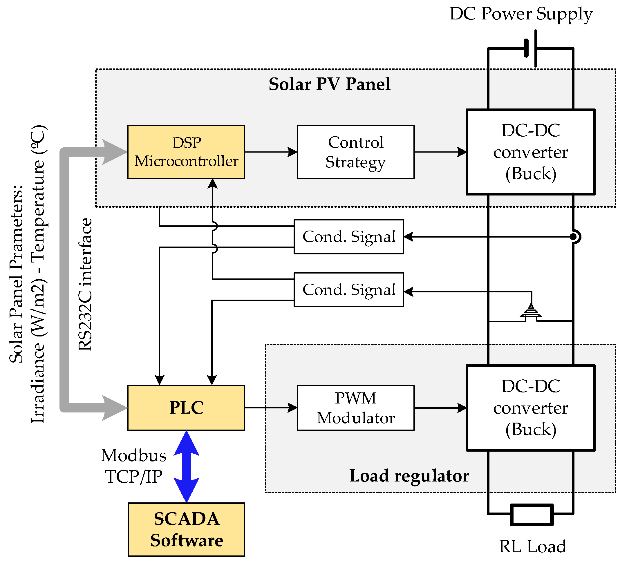
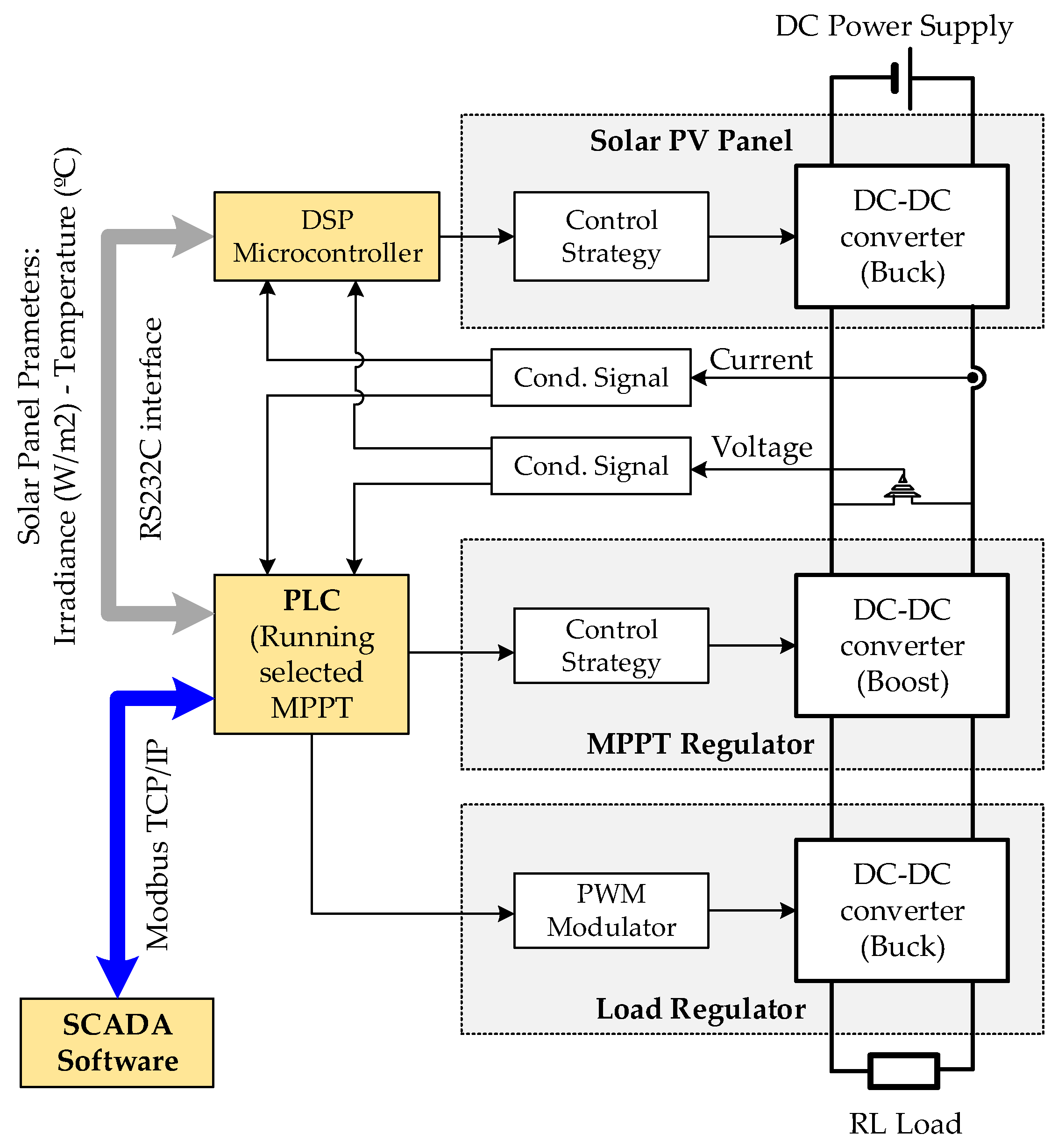
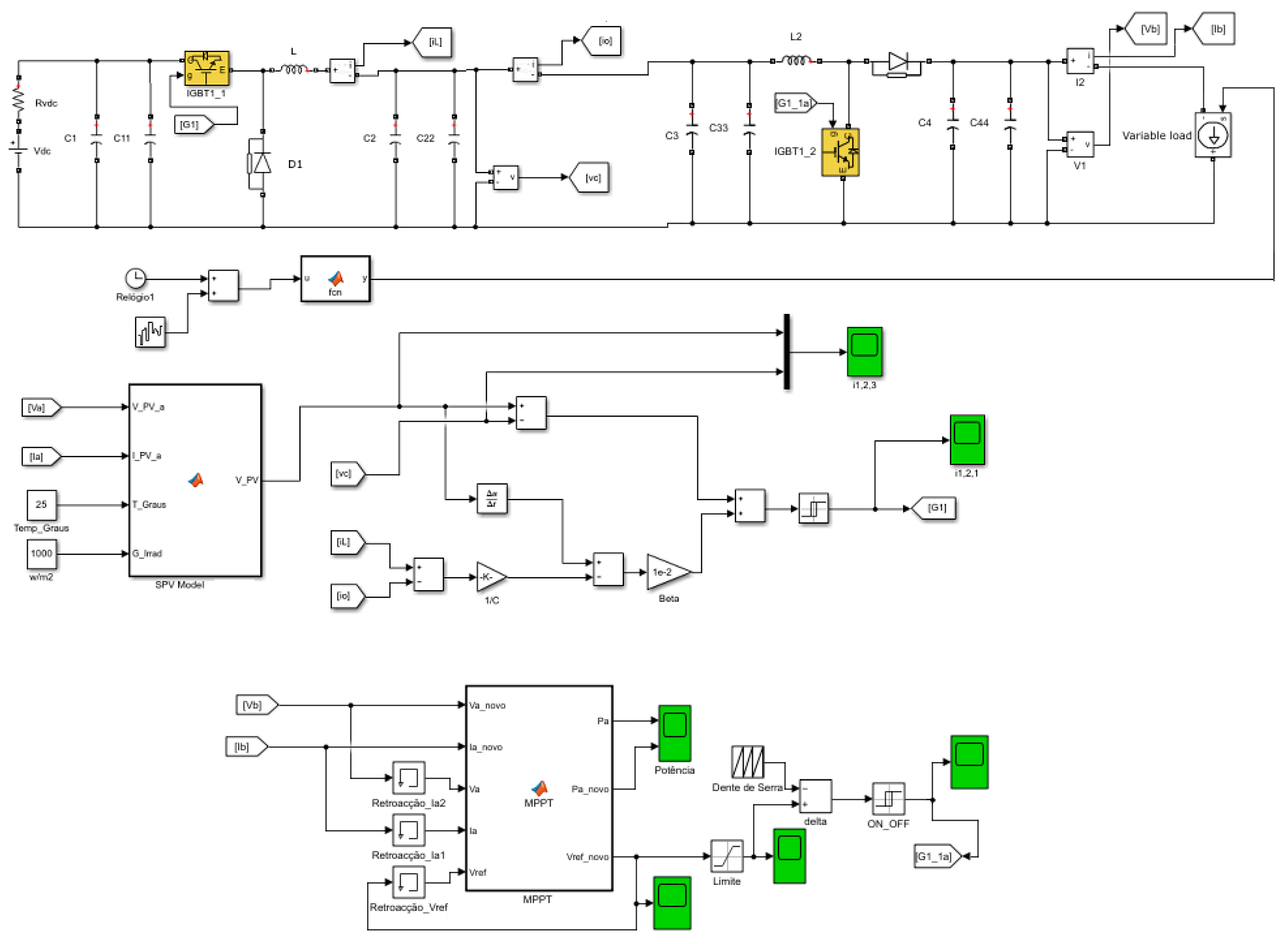
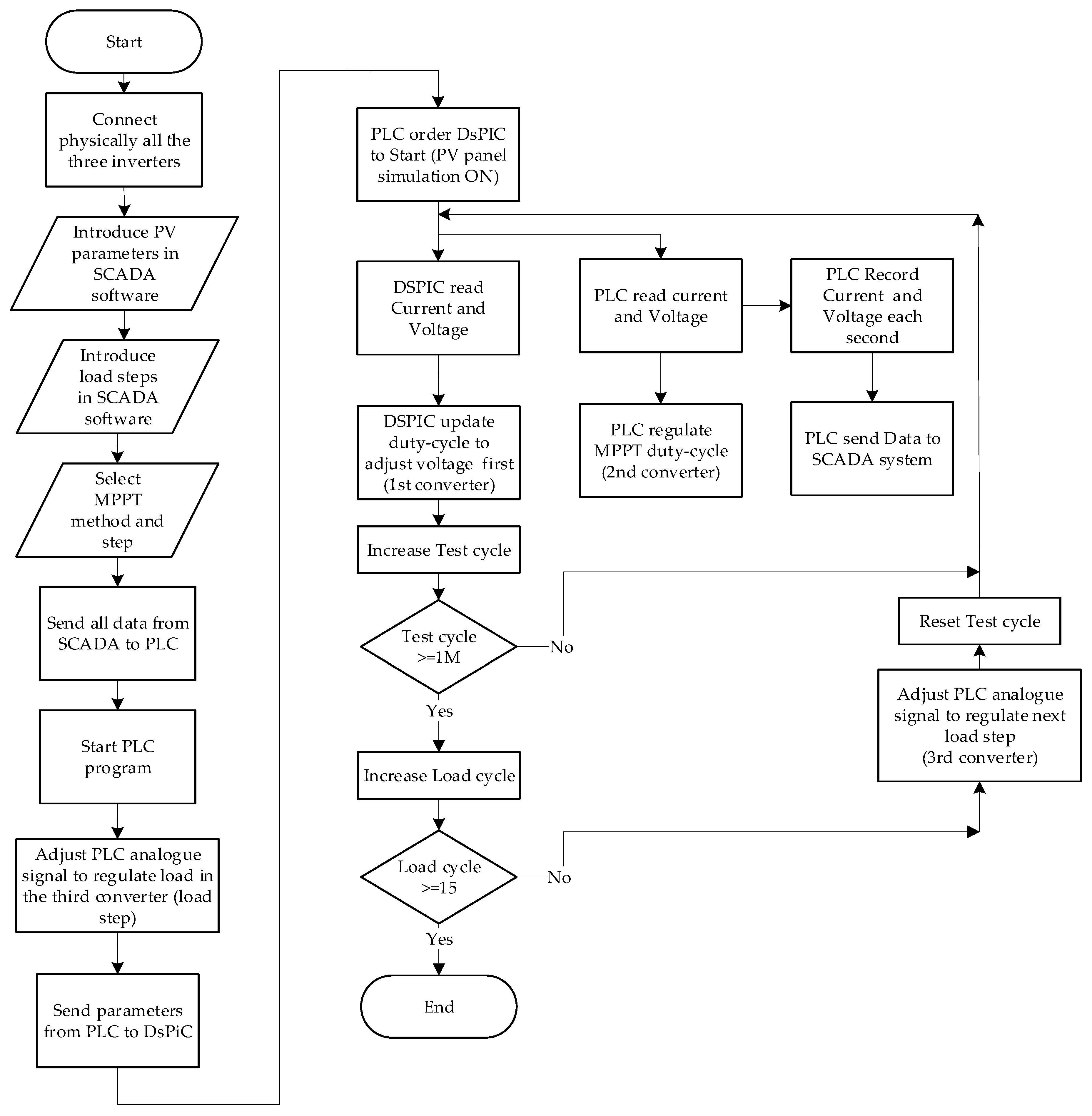
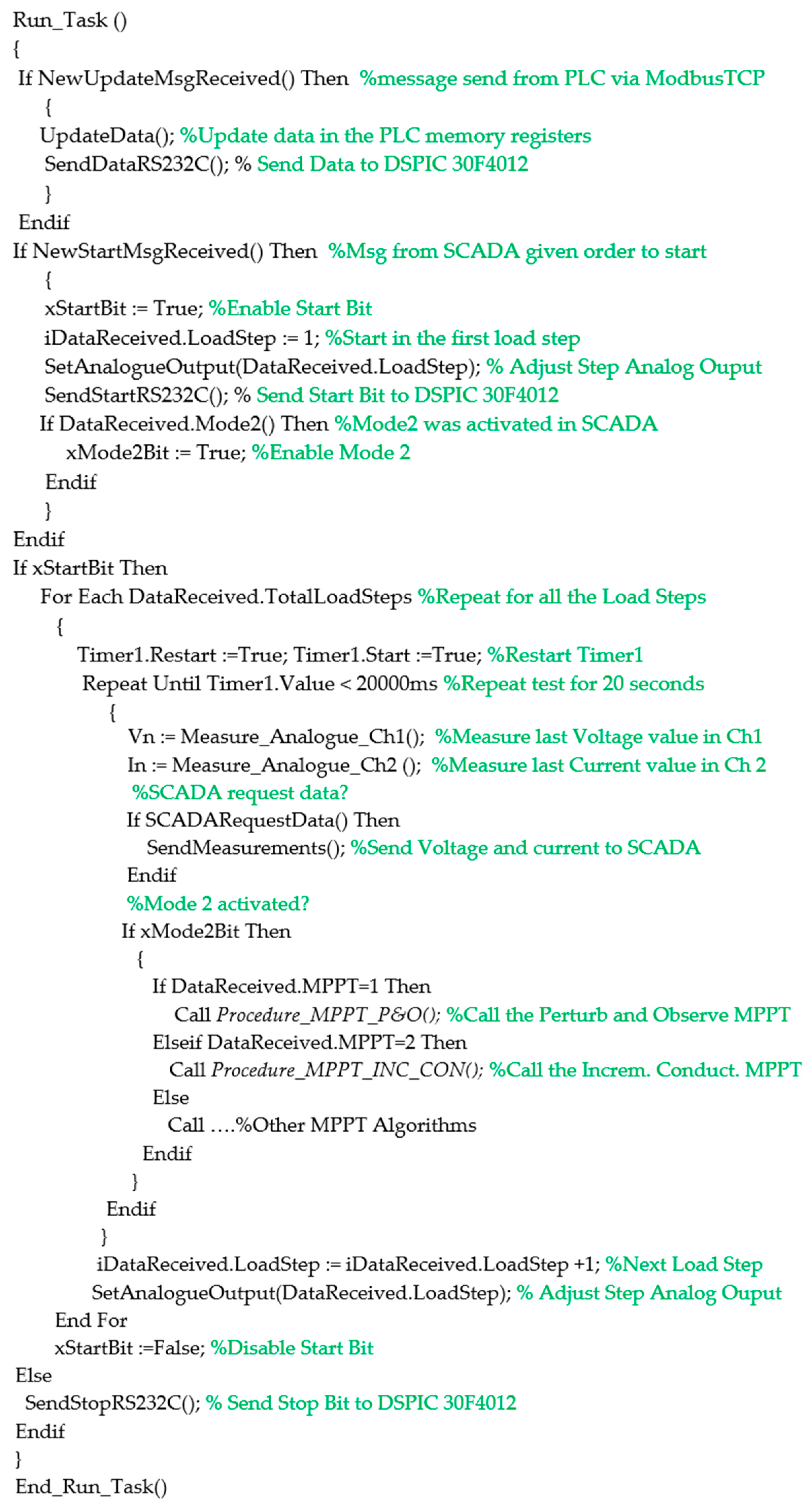
2. Description of the Proposed System

The main elements of this system are three buck–boost DC–DC converters, a regulated DC power supply, a DSP microcontroller, a PLC linked to supervisory control and data acquisition (SCADA) software, analog signal conditioning boards (current and voltage), a couple of analog sliding mode circuits, a PWM (pulse width modulation) modulator circuit, and an RL load. The system was developed to work in two separate modes. The first mode (mode I), or SPV panel mode, and the second mode (mode II), or MPPT test mode. Despite the same topology and components, the first and third DC–DC converters will operate in Buck mode and the second DC–DC converter will operate in Boost mode (see Figure 1).
Table 1 summarizes the operation modes of each converter.

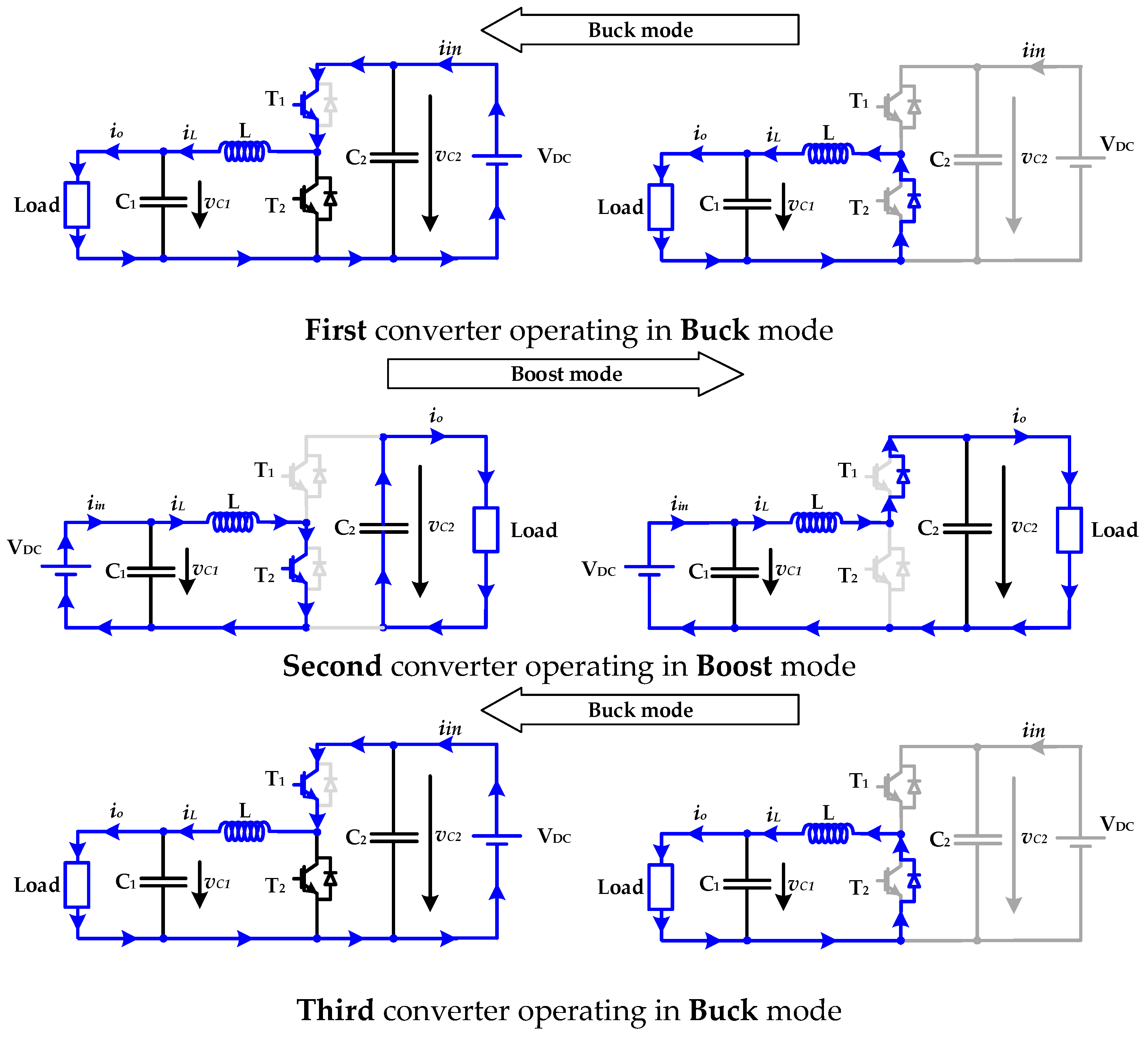
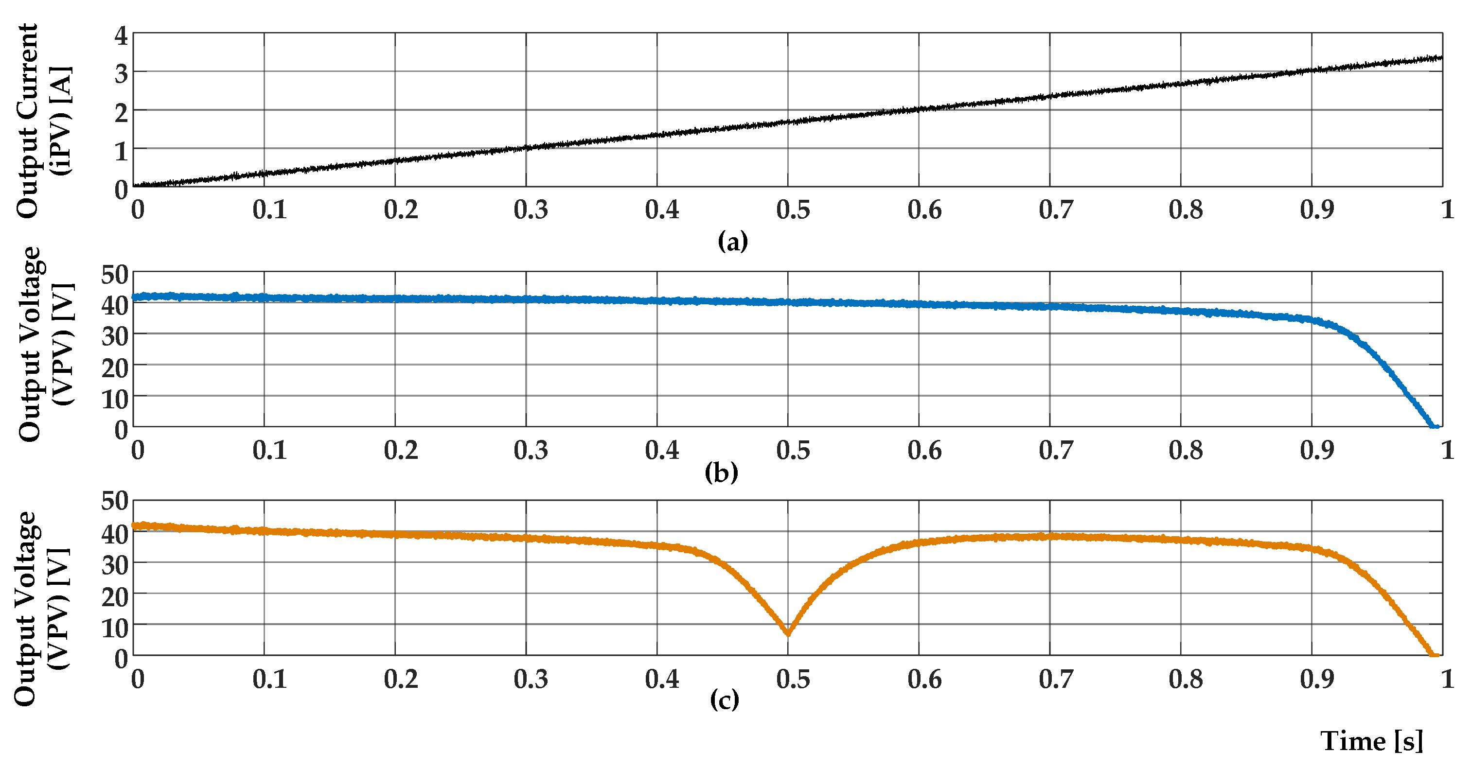
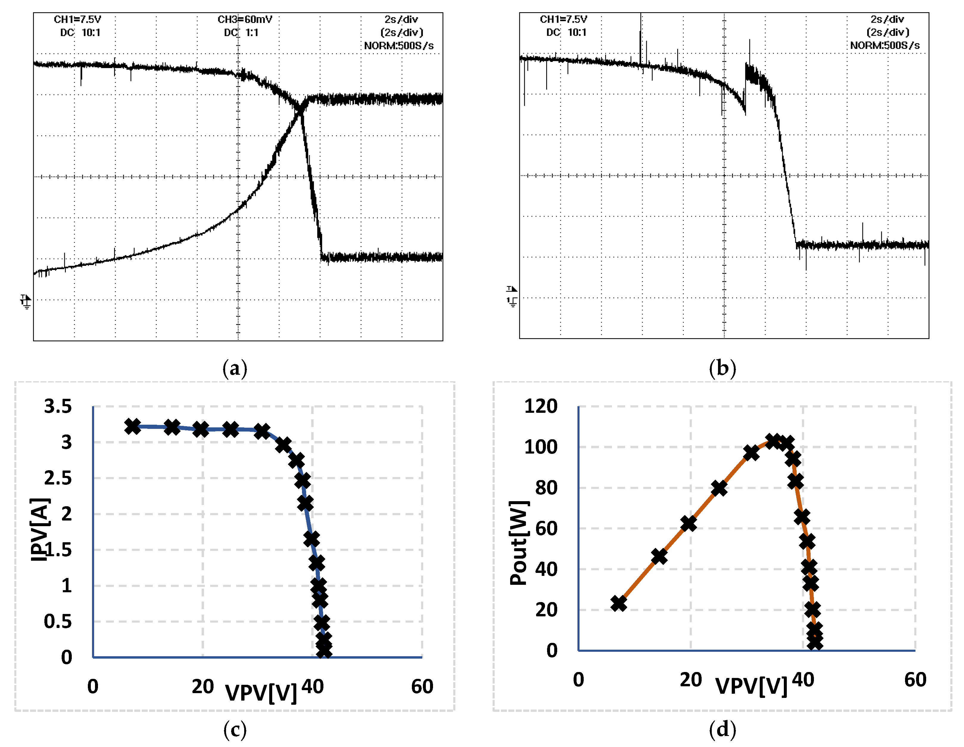
2.1. Mode I—Test and Emulate Characteristic I-V Curves

Figure 2 presents the general block diagram of mode I. Mode I is exclusively devoted to testing and emulating the characteristic I-V curves of the panel according to parameters provided by the manufacturer datasheet manual. Applying these parameters to an SPV model and considering different temperature reference and solar irradiance values, along with a variable load, it is possible to obtain the expected voltage and current of the SPV panel. In this mode are used only two DC–DC buck–boost converters (both in Buck operation mode). In this case, the first DC–DC converter simulates the SPV current and voltage panel, and the other DC–DC converter is used to perform load variation through PWM over a fixed RL load. This mode requires different stages to provide the correct operation. The first stage consists of adjusting the regulated DC power supply, the converter of which simulates the SPV panel. The next stage involves introducing the SPV panel parameters, the required temperature reference, and solar irradiance values in the SCADA software. Notice that the SCADA software was designed to accept SPV panels up to 365 W. Additionally, the SCADA software has the same SPV model of the DSP microcontroller and rejects data if they are out of range, avoiding creating problems in the controller and DC–DC converters. In this sense, the system is able to specify up to 15 variable load percentage values (to simulate the load variation at the terminals of the panel).
After validating the introduction of all the necessary information, the SCADA software will send the introduced data to the connected PLC using an Ethernet connection with Modbus TCP/IP protocol. The PLC collects all the information and sends the necessary data to the DSP device using a serial RS232-C interface. The information about load variation is used internally by the PLC to control the PWM of the third DC–DC converter (load regulator, see Figure 2). After processing all the information, the PLC starts the simulation of the SPV panel I-V curves. The PLC program is now able to automatically change the pre-specified step load reference 15 times during this process. During this process, the PLC records in the internal memory register the current and voltage feedback received by the analog interface. As current and voltage are continuously changing in the real DC–DC converters, the PLC also calculates the average values during each step. The progress of the simulations is continuously displayed in proper screen layouts using trend charts in the SCADA software. A flowchart of this operation mode is available in the experimental results sections among more details about software and hardware.

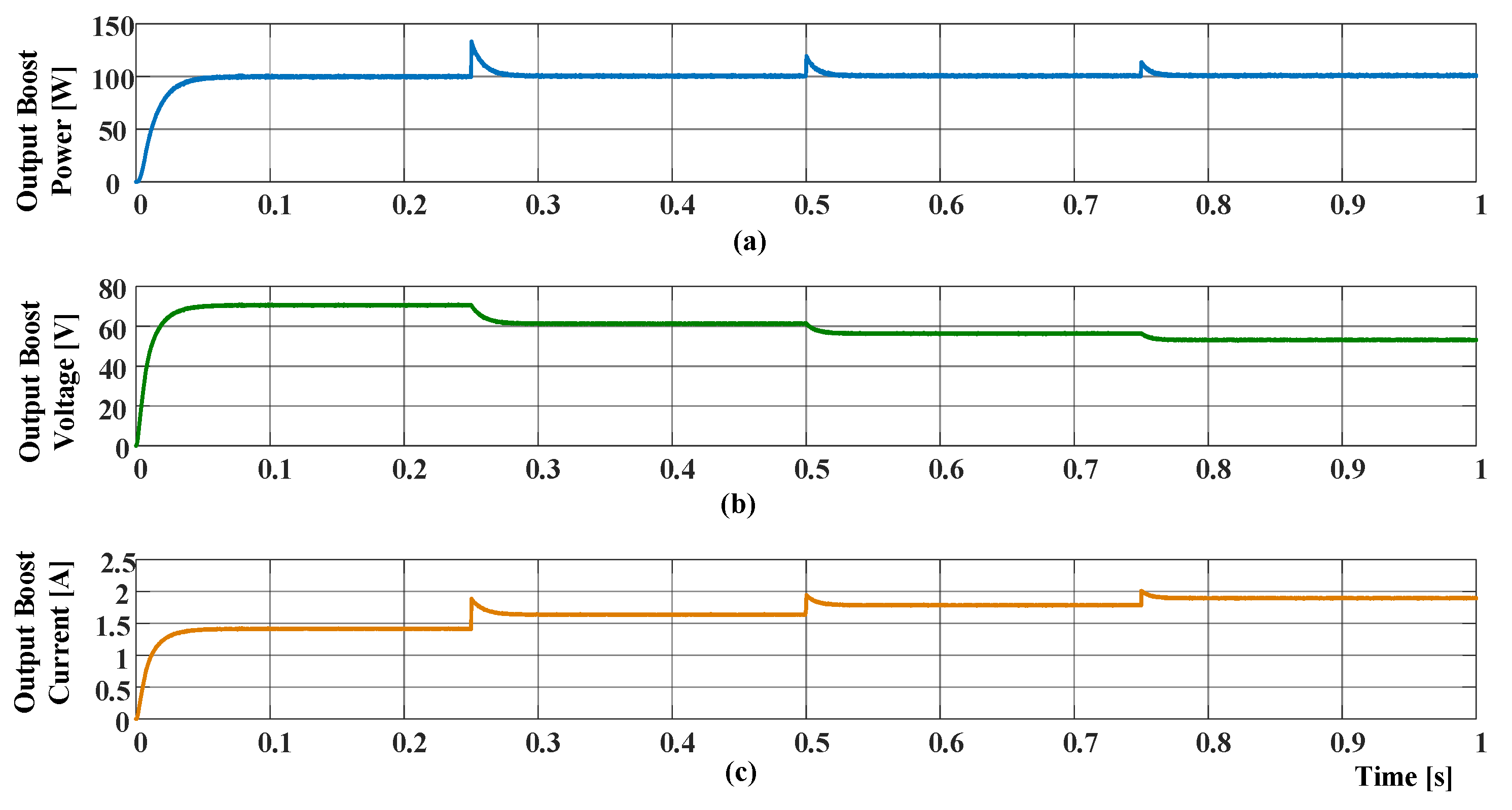
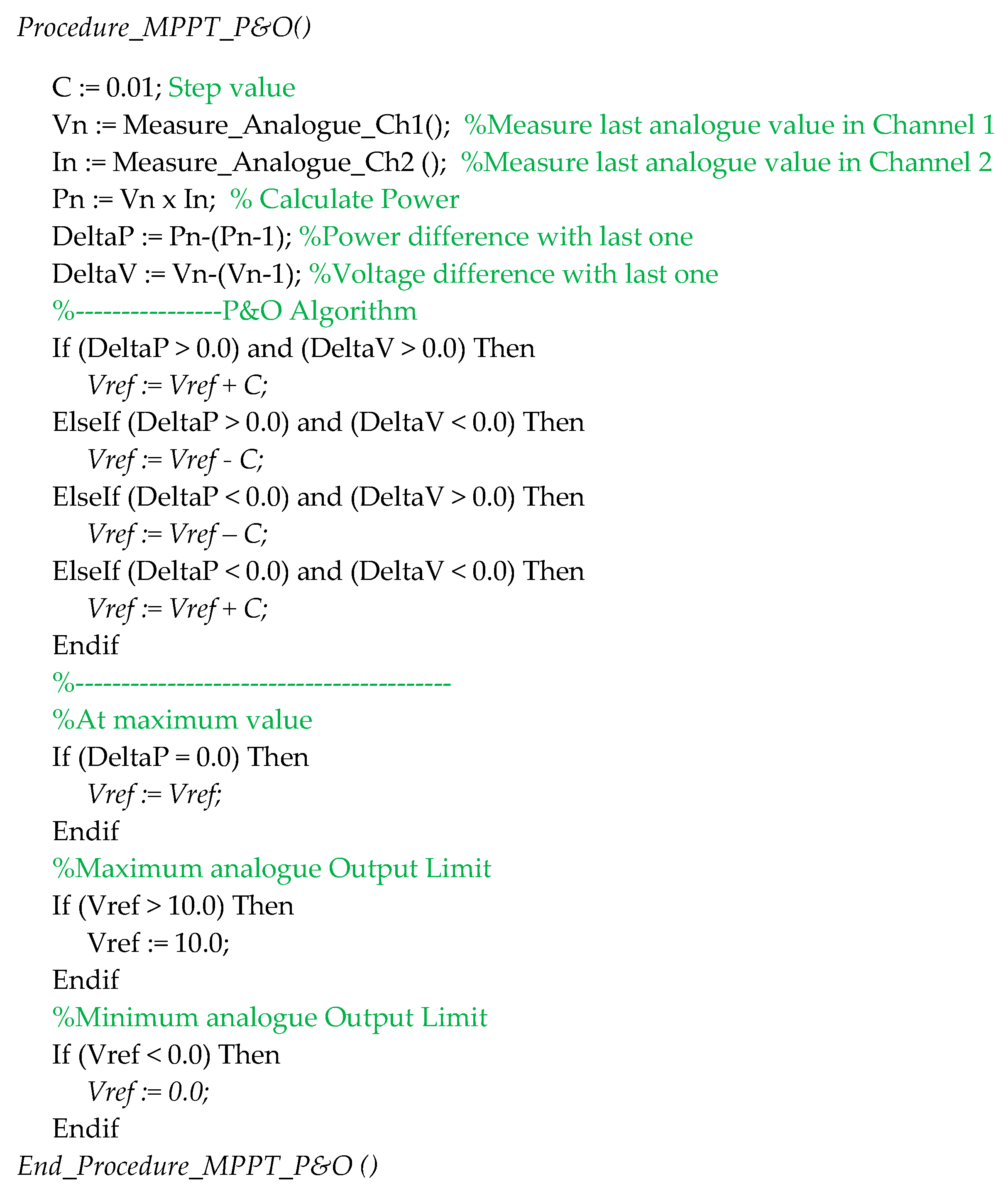
2.2. Mode II—MPPT Test Mode

The operational diagram block of mode II (or MPPT test mode) can be seen in Figure 3. This simulation mode introduces some additional features to mode I to test the MPPT control algorithm adopted and assess the produced power in several load conditions. For educational purposes, this provides the possibility to understand how to obtain the maximum power of an SPV (although not connected to the grid). In this simulation mode an additional DC–DC buck–boost converter is used, operating now in Boost mode (as described in Figure 3).
The procedures to operate in mode II are similar to mode I. Nevertheless, in this mode, in addition to all the introduced parameters specified in mode I, it is also necessary to select the preferred MPPT algorithm. In the proposed system, only two well-known MPPT techniques were effectively implemented, namely, hill climbing (HC) and perturb and observe (P&O) [26,27]. Theoretically, other MPPT techniques [28,29] can be implemented, although some of them are usually complex and require high-speed processors, which might not be compatible with the PLC adopted. An article presenting a modified fuzzy logic control algorithm for the extraction of maximum power through PV systems under severe climatic drifts can be found in [30]. Additionally, an MPPT algorithm using a modified incremental conductance technique in a grid-connected PV array is presented in [31]. The chosen techniques were selected due to their simplicity and efficiency for uniform solar irradiation conditions as the SPV will create only one global MPP in such conditions. A flowchart of this operation mode is available in the experimental results sections among more details about software and hardware.

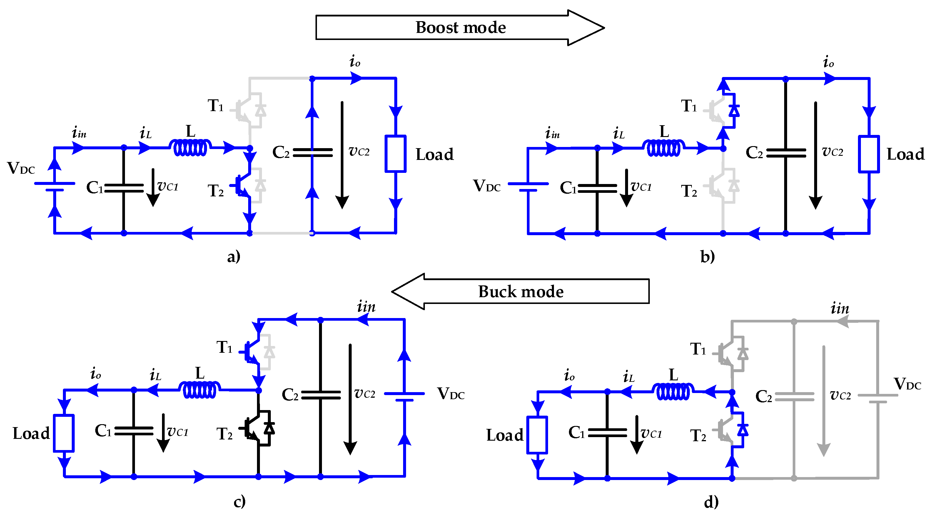
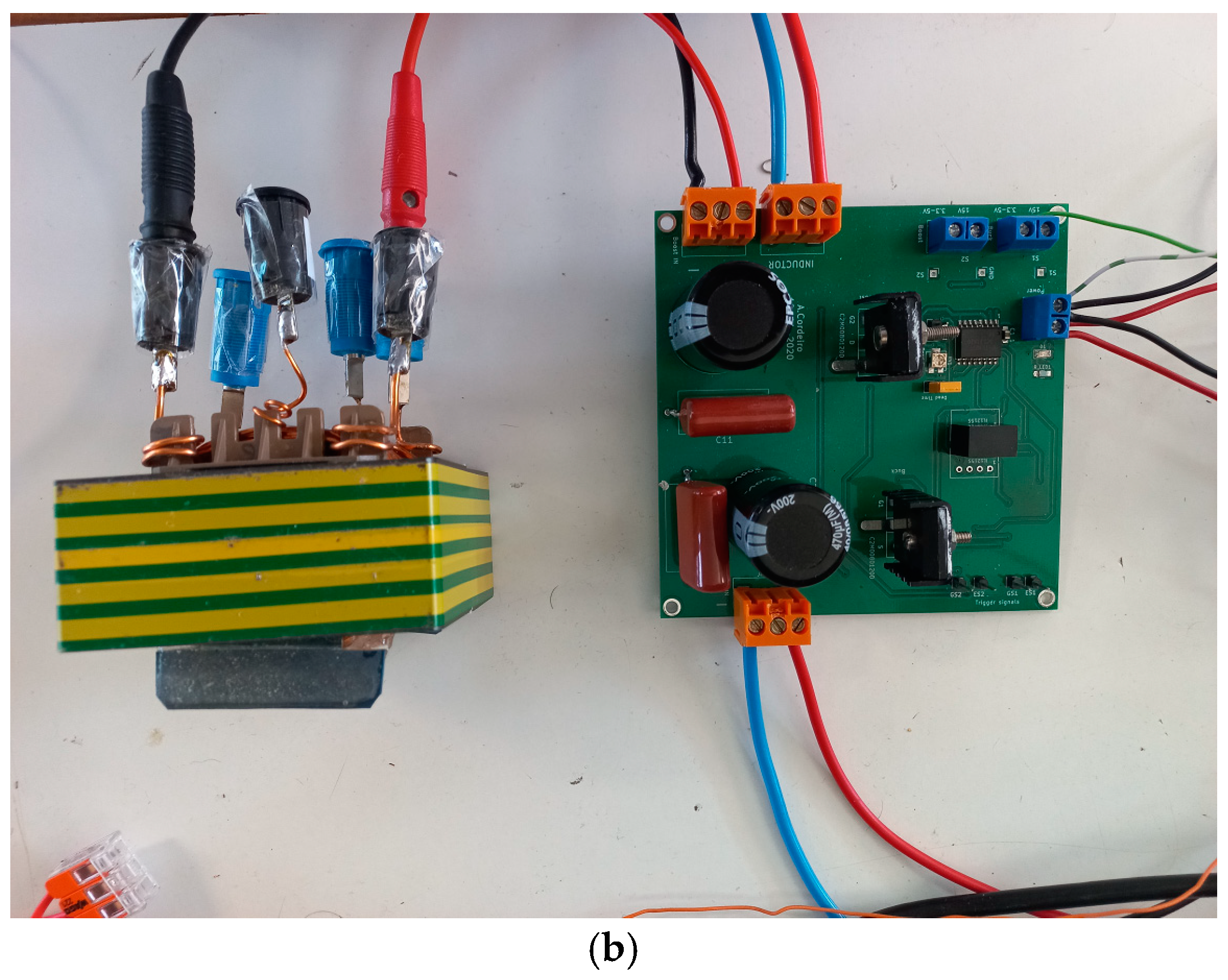
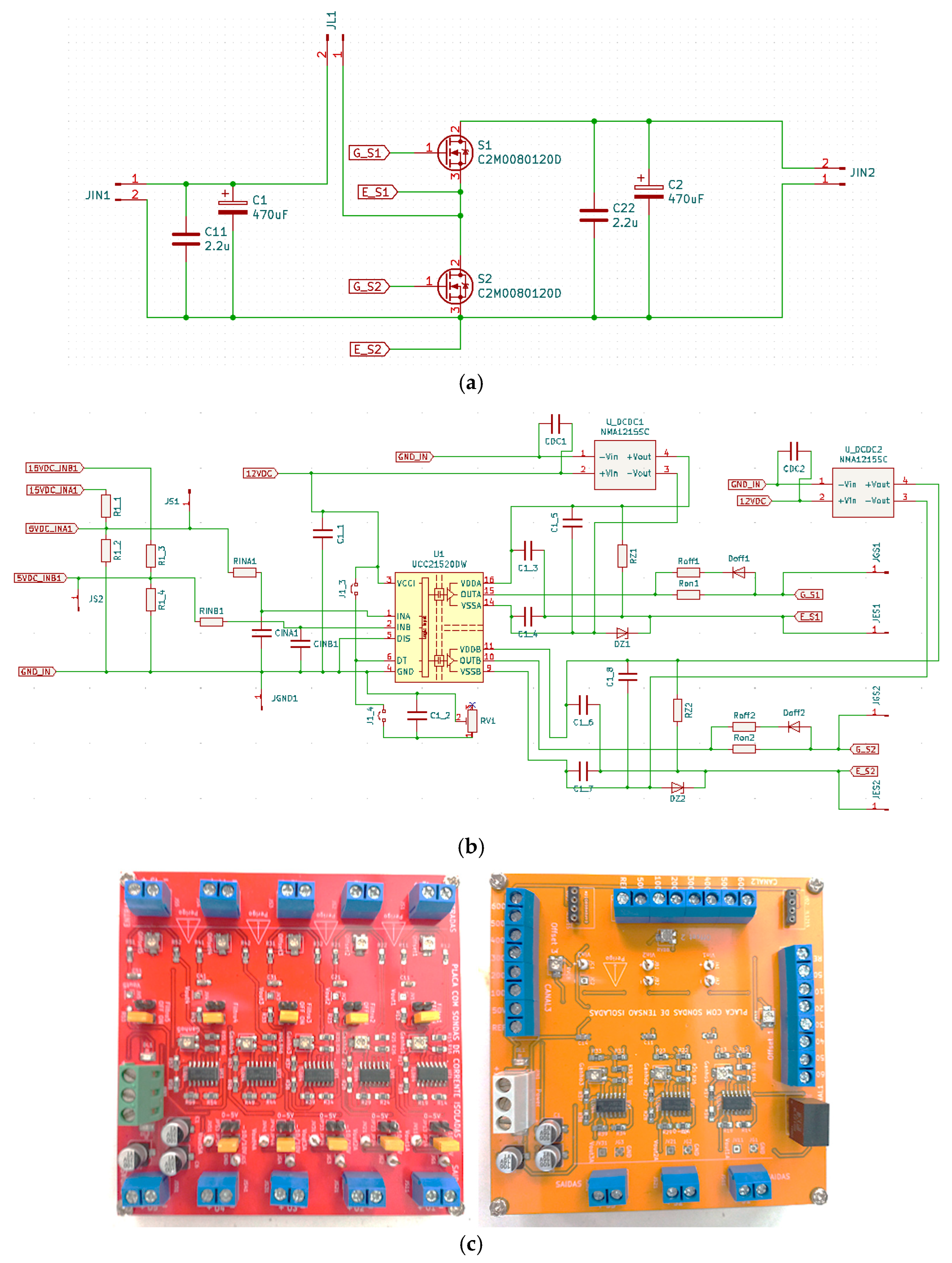
2.3. Converters Design

In this work, it was adopted a unique PCB board design with the classic buck–boost DC–DC power converter. The design allows to choose the desired Buck or Boost connection. The simplified diagram of this classic topology can be seen in Figure 4. Thus, by connecting this dual DC–DC converter from the left side to the right side (switching on T2 and turning off T1), the converter operates in Boost mode (Figure 4a,b). Reversing the load and power supply position operates in Buck mode (switching on T1 and turning off T2) (Figure 4c,d). Other topologies can be used with higher voltage gain and other characteristics, depending on the desired requirements. In the proposed work, it was considered that the classic buck–boost DC–DC converter was adequate for this purpose, as demonstrated by some experimental results.
The following sizing calculations, based on [32], are designed in two different conditions, the Buck and Boost modes. Despite the topology being the same, they were designed in different situations. The results achieve different minimum values for the output capacitor, but, in order to standardize the converter, the same components were adopted. The solution was designed to a maximum output power of 365W [33] using the maximum power of a connected SPV panel as described in the next table.
Designing the converter components in Buck mode (topology used as SPV simulator) requires knowing three parameters:
  • Input voltage VDC;
  • Minimum output voltage VOUT(min);
  • Maximum output current IOUT(max).
The first step is to calculate the maximum current flowing through the semiconductor, so it is necessary to know the maximum duty cycle in operation. In Equation (1), the efficiency is considered to obtain a more realistic duty cycle value. An efficiency value of η = 90% was considered as a worst-case scenario value for this buck converter. The VOUT(min) value considered in this condition is the voltage at the MPP of the SPV panel presented in Table 2. It was also considered an input voltage VDC = 60 V.
δ 1 = V O U T ( min ) η V D C = 33.6 0.9 × 60 0.62
With the duty cycle, it is now possible to obtain the inductor current ripple ∆IL, assuming a maximum switching frequency of fs = 20 kHz (this is the maximum frequency that the DSP device achieves) and an inductor value of L = 1 mH. The inductor current ripple is given by Equation (2).
Δ I L = V D C V O U T δ 1 L f s = ( 60 33.6 ) × 0.62 1 × 10 3 × 20 × 10 3 = 0.81 A
Knowing the MPP current (maximum current of the converter IOUT(max)) of the SPV panel, it is possible to calculate the peak current that the power semiconductor T1 and inductor L have to withstand, as per Equation (3).
I L ( max ) = Δ I L 2 + I O U T ( max ) = 0.81 2 + 10.75 11.16 A
In this mode, the power semiconductor T1 must withstand an average value given by (4).
I T 1 ( a v ) = I O U T ( max ) δ 1 6.66 A
Additionally, in this operation mode, the freewheeling diode D2 must withstand an average value given by (5).
I D 2 ( a v ) = I O U T ( max ) ( 1 δ 1 ) 4.08 A
The minimum output capacitor value C1, considering an acceptable voltage ripple ∆VOUT of 0.1V, is obtained using (6).
C 1 = Δ I L 8 Δ V O U T f s = 0.81 8 × 0.1 × 20 × 10 3 52 μ F
In order to standardize the converter, it was selected as a capacitor of C1 = 470 μF.
The design of the converter components in Boost mode (topology used as MPPT regulator) is similar to the previous one. Considering that both converters are connected in series, the average output current of the buck converter is the average input current of the boost converter around the same operation point. In fact, in the MPPT test mode, the boost converter imposes the current value on the buck converter. Thus, both power semiconductors T1 and T2 must withstand the same average value, and, consequently, they have similar duty cycles:
I T 2 ( a v ) = I T 1 ( a v ) I O U T δ 2 = I O U T ( 1 δ 1 ) δ 2 = ( 1 δ 1 )
In this condition, the output voltage of the boost converter is given by (8), considering again an efficiency value of η = 90%.
V O U T = V D C ( min ) η ( 1 δ 2 ) = 33.6 × 0.9 ( 1 0.38 ) 49 V
Calculating the duty cycle in this mode, it is possible to obtain the inductor current ripple ∆IL, assuming a fixed switching frequency of fs = 60 kHz and an inductor value of L = 1 mH. The inductor current ripple in the boost inductor is given by Equation (9).
Δ I L = V D C ( min ) δ 2 L f s = 33.6 × 0.38 1 × 10 3 × 60 × 10 3 0.21 A
In the above conditions, the peak current that the power semiconductor T2 and inductor L have to withstand is given by (10).
I L ( max ) = Δ I L 2 + I O U T ( max ) = 0.21 2 + 10.75 10.85 A
Additionally, in this mode, the freewheeling diode D1 must withstand an average value of (11).
I D 1 ( a v ) = I O U T ( max ) ( 1 δ 2 ) 6.66 A
The minimum output capacitor value C2 for the boost converter considering an acceptable voltage ripple ∆VOUT of 0.1 V is given by (12).
C 2 = Δ I L 8 Δ V O U T f s = 0.21 8 × 0.1 × 60 × 10 3 4.4 μ F
In order to standardize the converter, it was selected as a capacitor of C2 = 470 μF.
Other strategies to optimize the converter parameters for other topologies can be found in [34].

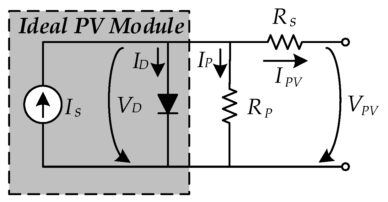
2.4. Mathematical Model

For this buck–boost converter, a mathematical model can also be developed in which the power semiconductors can be associated with a binary variable. Therefore, the first step for developing the model is to consider the binary variables α T 1 and α T 2 that are associated with the logical states of transistors T1 and T2 with the correspondent antiparallel diodes. These variables are described in (13) and (14)
α T 1 = 0 , T 1 O n D 1 O n 1 , T 1 O f f D 1 O f f
α T 2 = 1 , T 2 O n D 2 O n 0 , T 2 O f f D 2 O f f
Using the referred binary variables, it is now possible to write the converter model as presented in (15) and (16). The model given by (15) is for the Boost mode, whereas the other model (16) is for the Buck mode. In these equations, iL is the inductor current, io is the output current, vDC is the converter input voltage, vC1 is the voltage over of the output converter capacitor (Buck mode), and vC2 is the voltage over of the output converter capacitor (Boost mode).
d i L d t d v C 2 d t = 0 α T 1 α T 2 α T 1 α T 2 0 i L v C 2 + v D C i o
d i L d t d v C 1 d t = 0 1 1 0 i L v C 1 + α T 1 α T 2 1 v D C i o

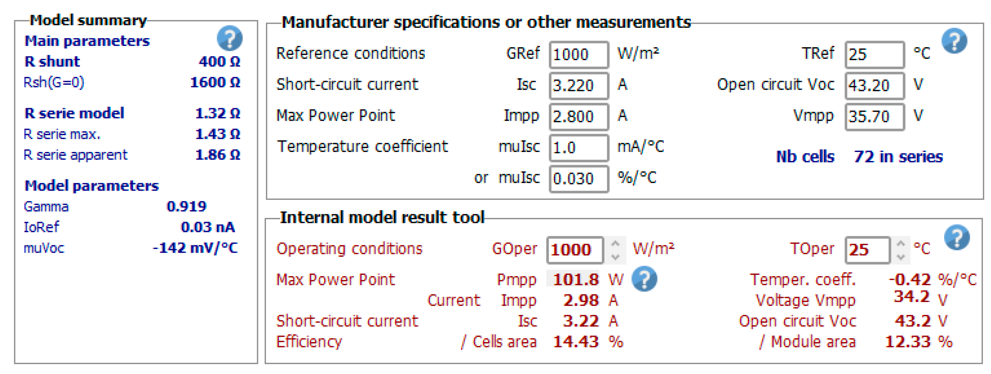
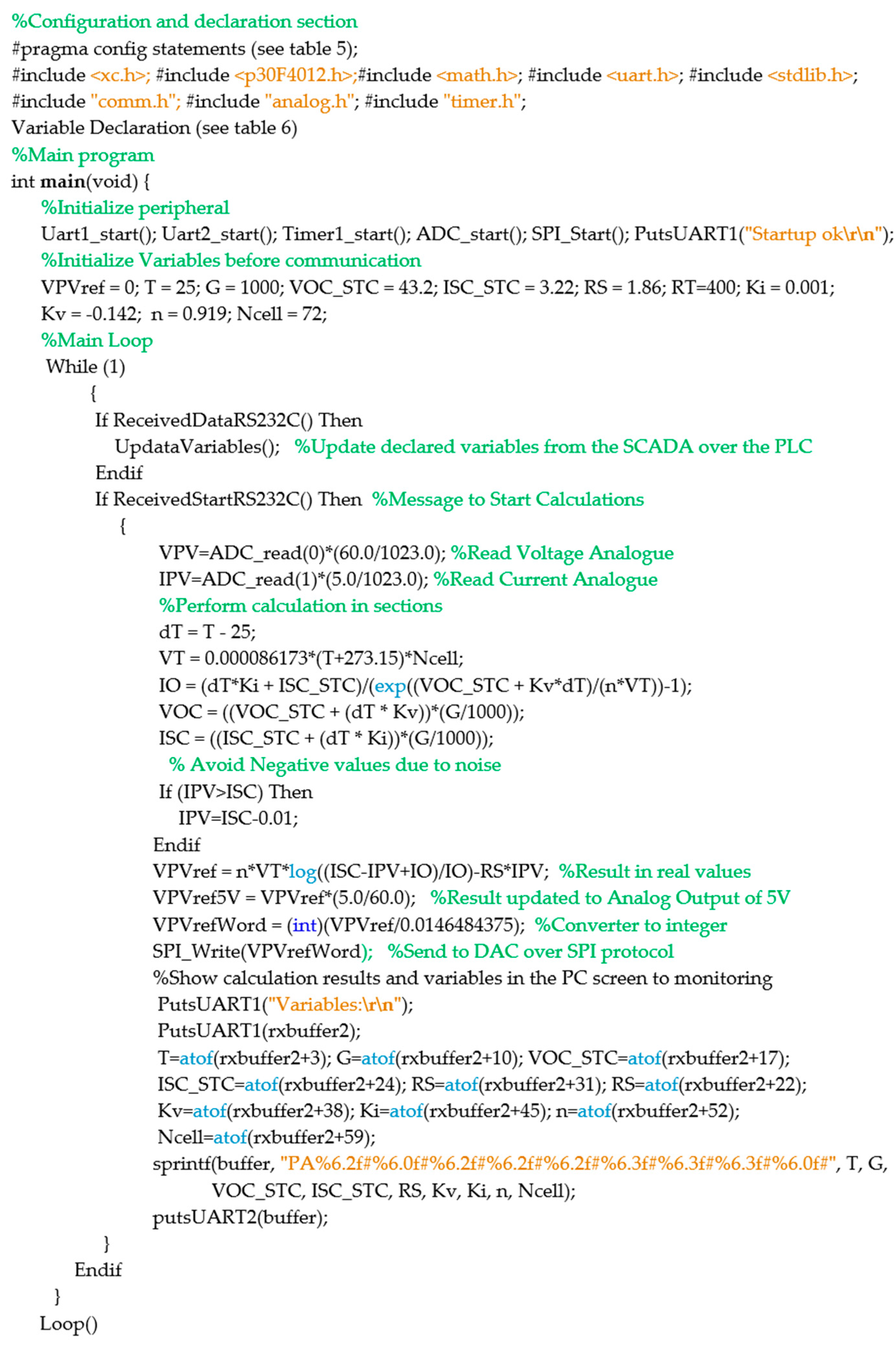
3. SPV Model Adopted

As mentioned in the previous section, the SVP panel is simulated using a DC–DC buck–boost converter. This DC–DC buck–boost converter must operate as a buck converter and must be able to generate an output voltage at the terminals of the output capacitor C1, similar to an SPV panel (as described in Figure 4c,d). Thus, the control system must be able to impose reference values on the power converter to generate the I-V characteristic curve according to the manufacturer’s parameters. The adopted SPV model is based on the single-diode model [21] which is one of the most used by academics and industry. This model produces a fairly accurate result and has a low computational cost [35]. This model, instead of a nonlinear I-V characteristic approximated as 2n order line segments, modeled as n diodes connected in parallel (creating a piecewise linear approximation, by sections), proposes a single approximated nonlinear I-V characteristic much more accurately. Identifying the five unknown parameters, namely, the ideal SPV current IS, the diode saturation current I0, the ideality factor α, the series resistance RS, and the parallel resistance RP, the output current–voltage characteristic can be modeled. Figure 5 shows the equivalent circuit of the single-diode model. In this simplified model, IS represents the ideal photocurrent as a result of a certain light intensity G and cell operating temperature, and the single diode represents the diffusion phenomena where a dark current ID flows. In this model, IP represents the current flowing across the parasitic parallel equivalent resistor caused by P-N junction imperfections. The serial resistance RS represents the sum of resistances of the serially connected cell layers and contacts between both ends of the SPV panel.
The terminal current IPV of the single diode model for the SPV panel from Figure 4 can be written by combining all the currents with Equation (17). All these elementary currents will be defined over the next equations.
I P V = I S I D I P
The value of the ideal photocurrent IS at a temperature reference of T = 298.15 K (≈25 °C) and an irradiation reference of GR = 1000 W/m2 is given by Equation (18). In this equation, ISC is the equivalent short circuit current, and ki is the short-circuit current coefficient [13].
I S = I S C + k i ( T S T ) G G R
In this model, the dark current ID (Equation (19)) depends on several parameters, namely, the reverse saturation current I0, the output voltage VVP, the output current IPV, the number of SPV cells connected serially NS, Shockley’s diode ideality factor α, and the thermal voltage of the SPV module VT (Equation (20)). In turn, the thermal voltage depends on the Boltzmann constant k = 1.3806 × 10⁻²³ /K, the reference temperature T = 298.15 K (≈25 °C), and the elementary electron charge q = 1.6022 × 10⁻¹⁹ C. The reverse saturation current Io is expressed by Equation (21), where Eg ≅ 1.1 eV is the gap energy for Si semiconductors, and Irr represents the reverse saturation current at the temperature reference. This current is also dependent on the module cell operating temperature TS.
I D = I O exp V P V + I P V R S α N s V T 1
V T = k T q
I 0 = I r r T S T 3 exp q E g α K 1 T 1 T S
The current flowing across the parasitic parallel resistor is described by Equation (22).
I P = V D R P = V P V + R S I P V R P
Through the arrangement of Equations (17)–(22), it is possible to obtain the estimated value of the output current IPV (Equation (23)).
I P V = I S I O exp V P V + R S I P V α N S V T 1 V P V + R S I P V R P

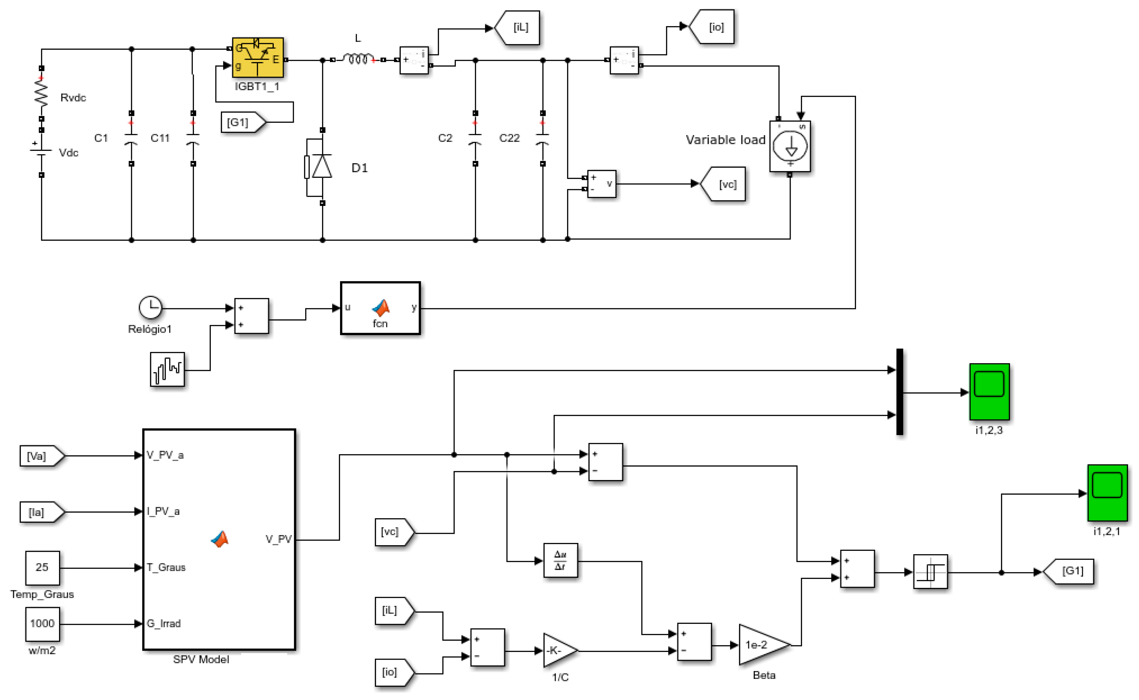
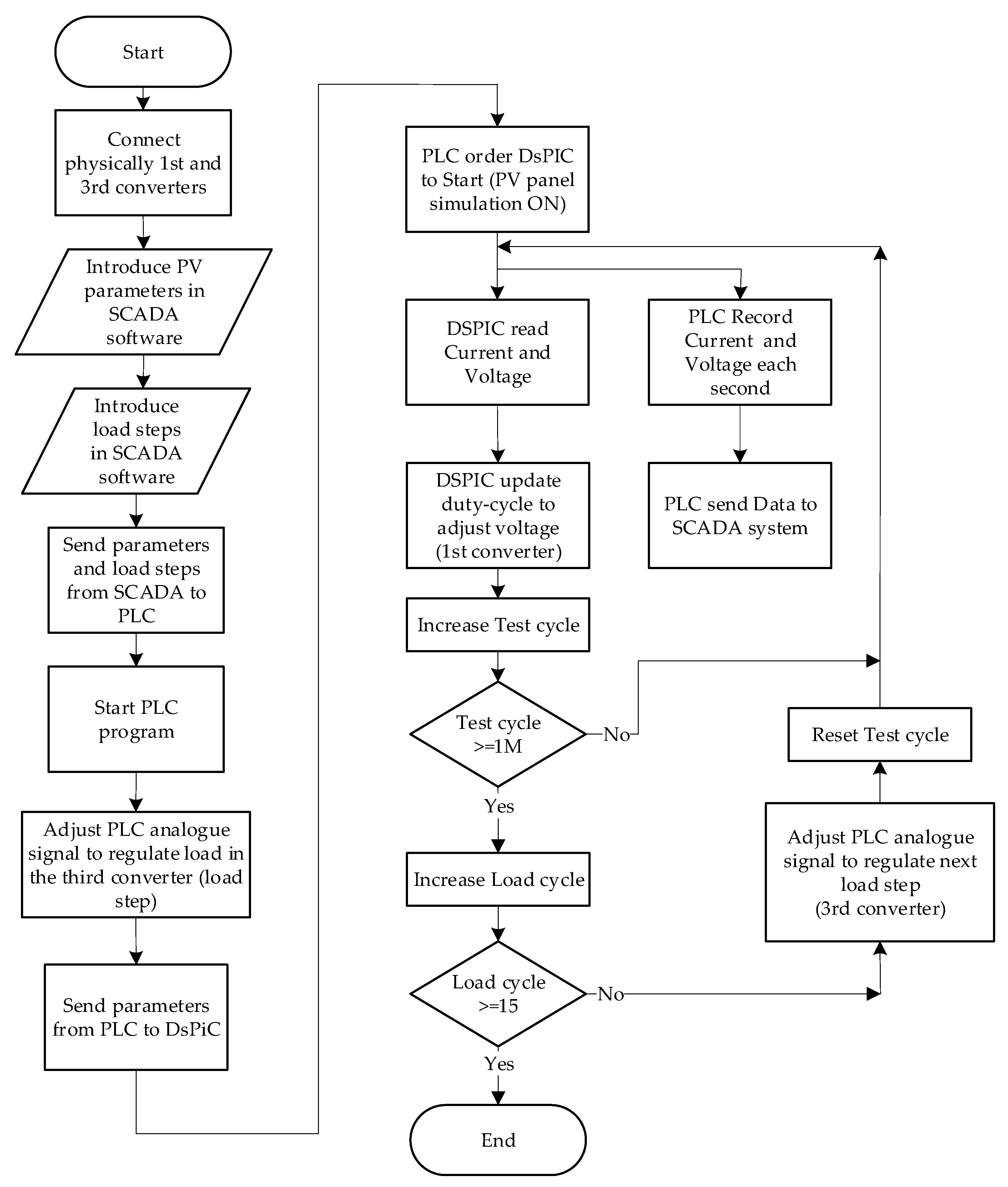
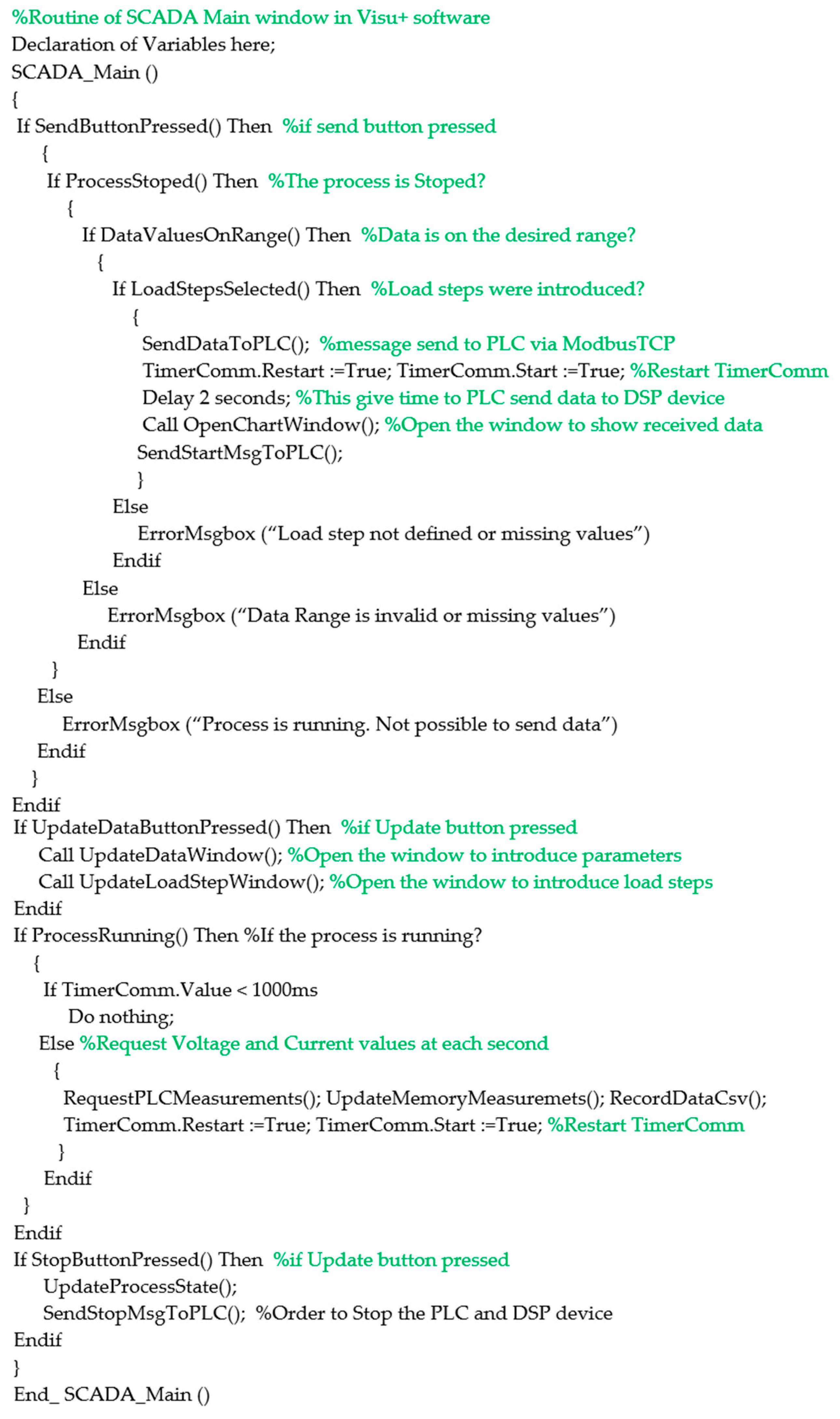
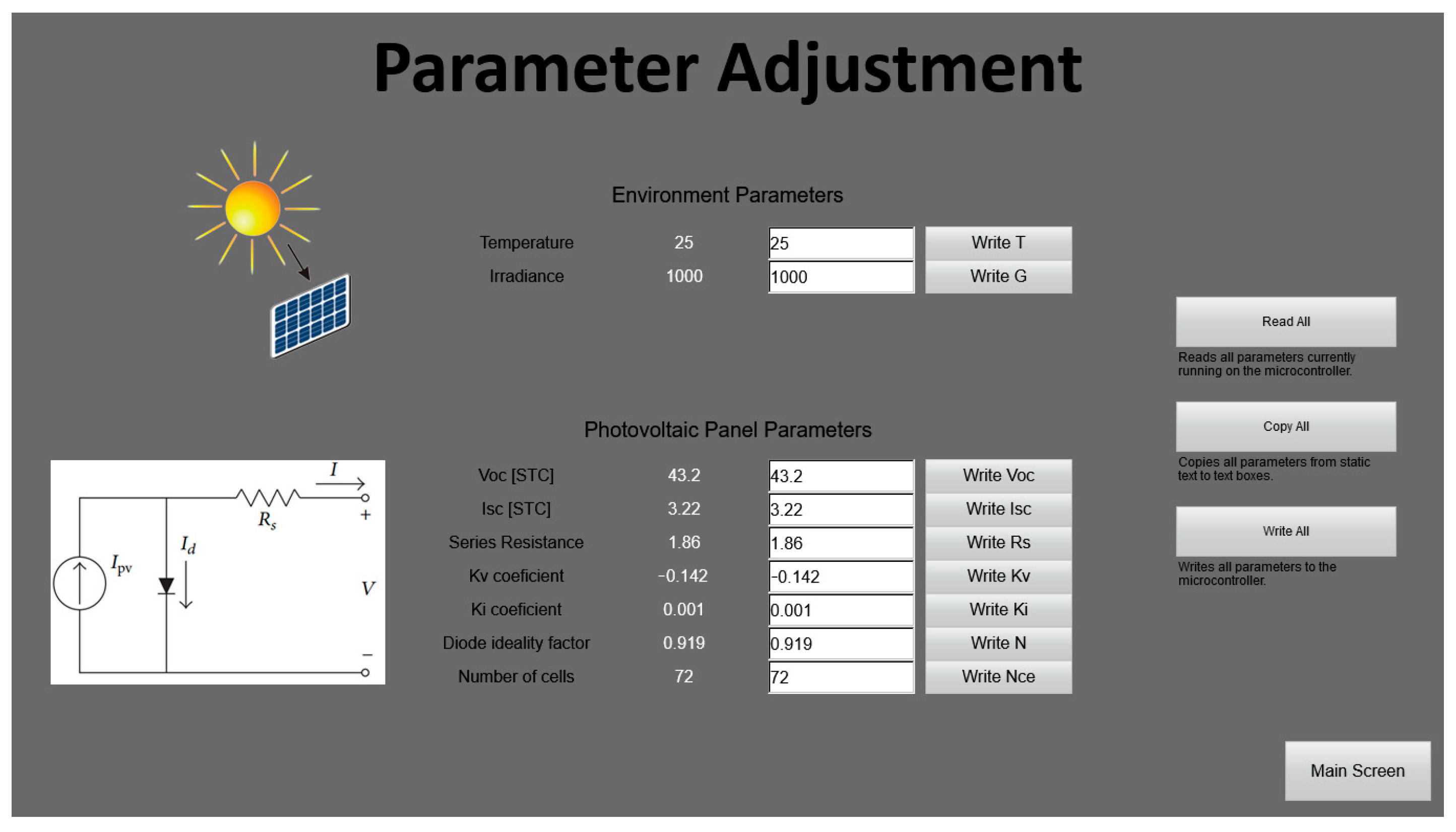
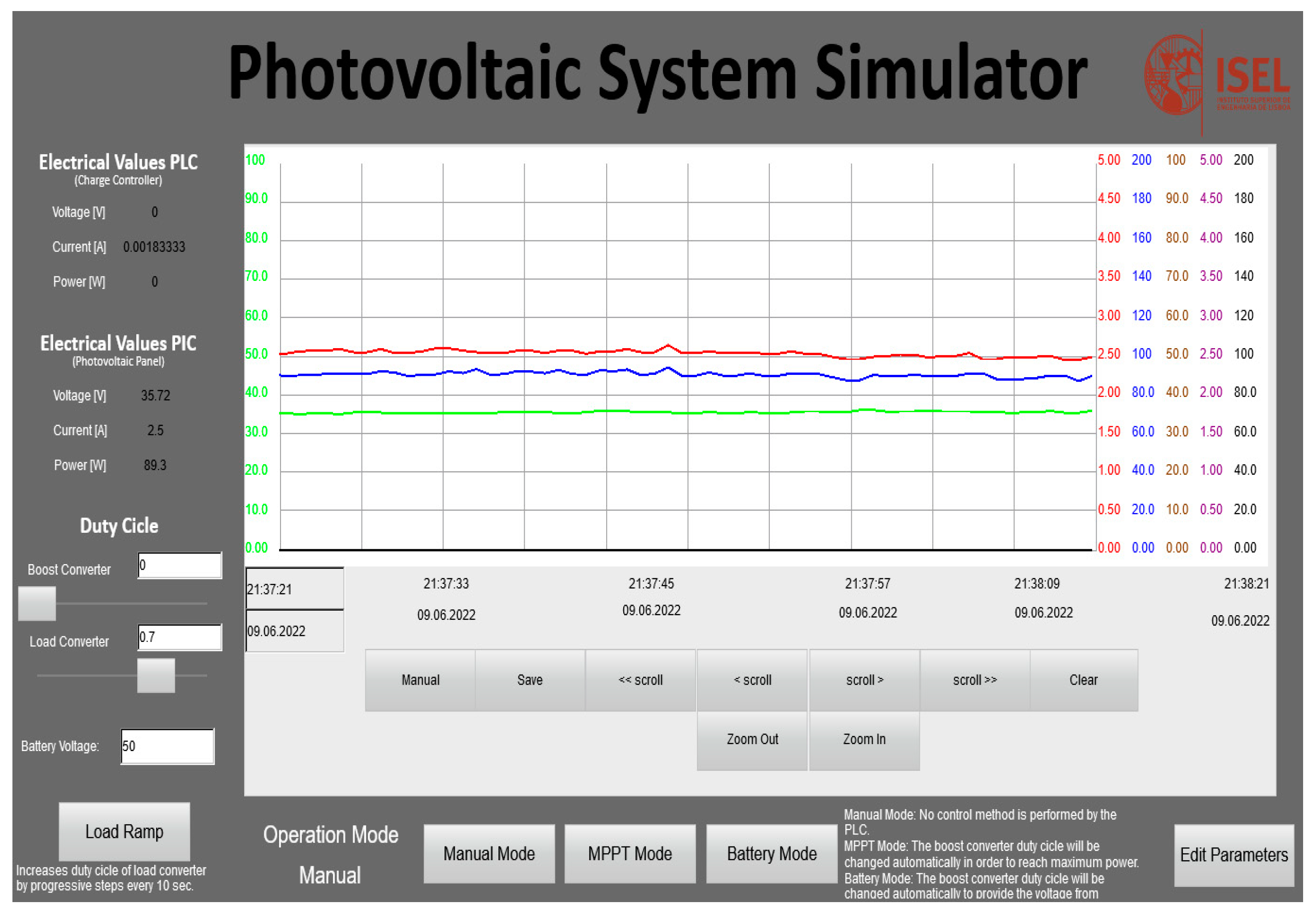
4. Control of the SPV Panel Simulator

The DC–DC buck–boost converter responsible for generating the current–voltage characteristics will be controlled using a sliding mode control technique. The sliding mode control technique presents a fast dynamic reaction and robustness to parameter and load variation [36,37,38] and has been widely used in numerous renewable energy applications [39,40]. To project this sliding mode controller, it is considered a dynamic model with ideal components, namely, the power transistor, inductor, and capacitors. The switching state of transistor T1 is described by the time-dependent switching variable λ, as shown by Equation (24) [41].
λ = 1 , T 1 T u r n e d O n 0 , T 1 T u r n e d O f f
Examining the correspondence between the voltages and the currents shown in Figure 3c,d, it is possible to obtain a simplified switched model of the DC–DC converter state-space, regarding the controllable variables iL and vC1 (Equation (25)) [41].
d i L d t = 1 L v C 1 + λ L v D C d v C 1 d t = 1 C 1 i L 1 C 1 i o
where L is the converter inductor, C1 is the output converter capacitor in Buck mode, vC1 is voltage over of the output converter capacitor, iL is the inductor current, io is the output current, and vDC is the converter input voltage.
Considering vC1 as the desired controlled output voltage, it is possible to rearrange Equation (25) considering the canonical controllability form, which is expressed by Equations (26) and (27). Notice that the output current i0 in Figure 4b is equivalent to the output current IPV of Figure 5, and vC1 in Figure 4b is equivalent to VPV in Figure 5, where ϕ is the voltage derivative over the time of the capacitor C1 [41].
d d t v C 1 ϕ = ϕ 1 L C 1 v C 1 1 C 1 d i o d t + λ L C 1 v D C
ϕ = i L i o C 1
From the state-space equation presented in (26), it is possible to realize that i0 has a strong relative degree of two [37] (which means that the controllable variable is obtained by the second time derivative). Thus, in this condition, the sliding surface specified in (28) is sufficient to ensure the necessary stability and robustness of the closed-loop control system as given by [38]. Parameter β defined in (28) is associated with the time constant of the first-order response of the input current (β > 0). Based on (26) and (28), it is now possible to define a theoretical sliding surface as described by Equation (29).
S e v C 1 , e ϕ = v C 1 r e f v C 1 + β ϕ r e f ϕ
S e v C 1 , e ϕ = v C 1 r e f v C 1 + β d v C 1 r e f d t β C 1 i L i o
However, in terms of the DC–DC power converter, it is necessary to impose a limited bandwidth on the gate drive due to the limited switching frequency of power transistors. In practical applications, this is usually undertaken using a hysteresis comparator which maintains the sliding surface near zero with a restricted switching frequency. Finally, the control law for transistor T1 is given by Equation (30), where ∆ introduces restrictions to the switching frequency.
i f S e v C , e θ > Δ o r S e v C , e θ < 0 a n d S e v C , e θ < Δ t h e n T 1 T u r n s O n ; i f S e v C , e θ < Δ o r S e v C , e θ > 0 a n d S e v C , e θ < Δ t h e n T 1 T u r n s O f f ;

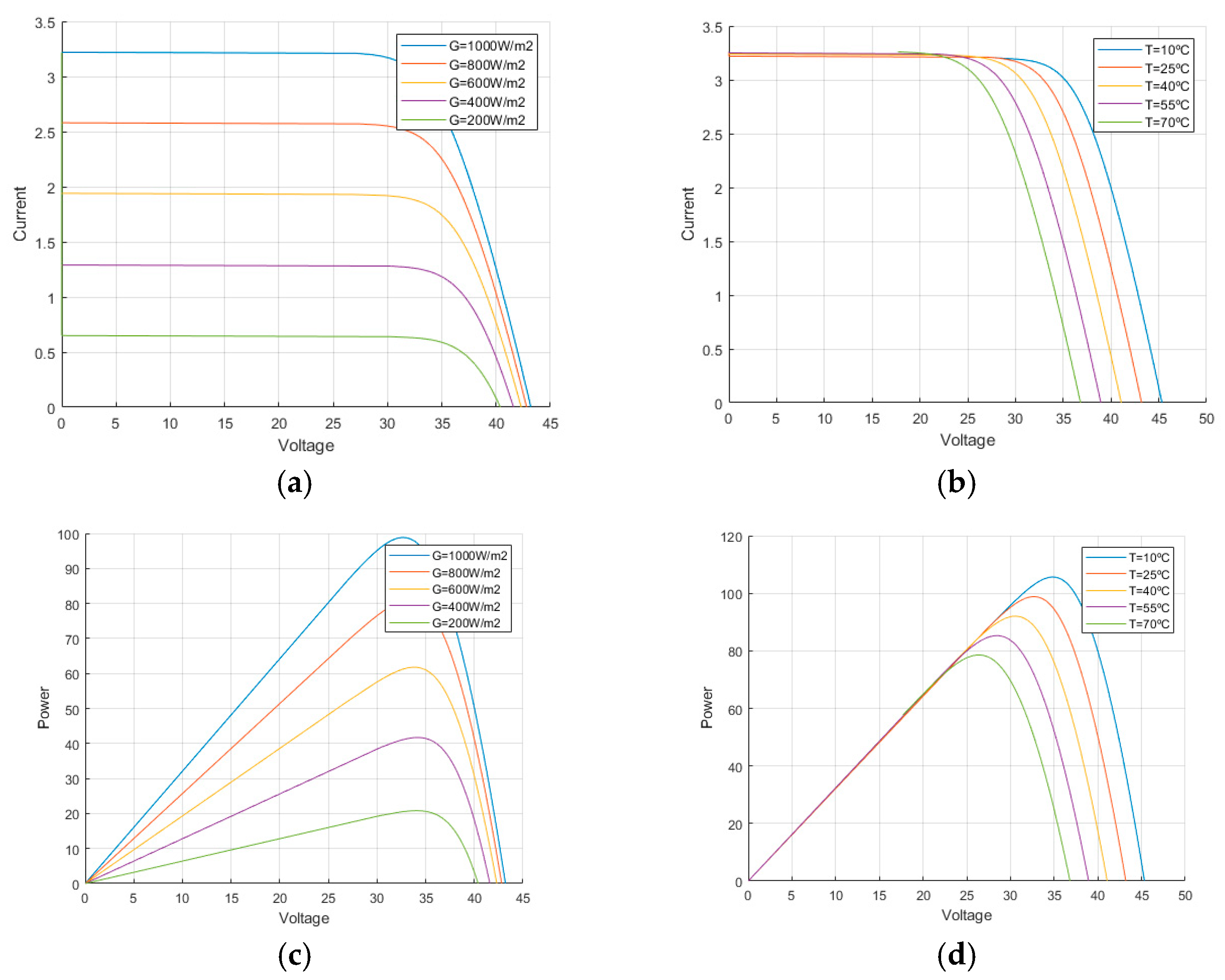
5. Simulation Results

To simulate the operation of the proposed system, MATLAB/Simulink software was used. Regarding the buck–boost DC–DC converter to simulate the SPV panel, the model presented in Section 3 combined with the sliding mode control strategy described in Section 4 was selected. The parameters for this model were obtained from the ASE-100-GT-FT Schot Solar Panel datasheet available online [42]. It is also possible to obtain parameters from several SPV panels using the PVsyst software database [43], as presented in the screenshot example of Figure 6.
According to the data available, (see Figure 7) the I-V and P-V characteristic curves for different irradiation values and operating temperatures were previously plotted. These results are only used for the purpose of testing the equations and parameters of the chosen SPV. Such simulation results are useful to compare with the experimental results presented in the next section.
The first simulation tests were created in test panel mode (mode I) to obtain different characteristic curves of the chosen SPV panel and evaluate the voltage and current variation. The selected components for the DC–DC converters used in the simulations are described in Table 3.
According to the proposed control of the SPV panel simulator presented in Section 4, a simulation test to evaluate the performance of the proposed simulator was developed. Figure 8 shows the simulation diagram, based on Equation (23), in MATLAB/Simulink of the proposed SPV simulator using the buck converter.
Figure 9 presents the result of a simulation test where a continuous load variation was performed to obtain the voltage variation at the terminals of the DC–DC converter. In Figure 9a, it is possible to see the continuous current variation, and Figure 9b shows the voltage variation considering fixed values of G = 1000 W/m2 and TS = 25 °C. Figure 9c shows the simulation test of the voltage variation considering that initially G = 600W/m2, and at t = 0.5 s, a step to G = 1000 W/m2 was produced. Notice that in this last simulation test, the system increases the voltage after t = 0.5 s and drops again with the increase in the current load, similar to Figure 9b. This shows that the output voltage increases with solar irradiation and decreases when the load increases, as expected.
Some simulation tests were also performed in MPPT test mode (mode II) to evaluate the dynamic response of the MPPT algorithm chosen (in this case, the P&O). Similarly, the parameters are those proposed in Table 3. Figure 10 shows the simulation diagram in MATLAB/Simulink to simulate mode II.
The simulation result of this test is shown in Figure 11. Based on this result, it is possible to observe that, despite the attempt to perform a load variation at 0.25 s, then at 0.5 s, and finally, at 0.75 s, the proposed solution always supplies the load with approximately 100 W due to the MPPT algorithm running in the PLC and consequent PWM signal applied to the DC–DC converter. Notice that the simulation waveforms shown in this figure correspond to the output values of the converter operating in Boost mode.

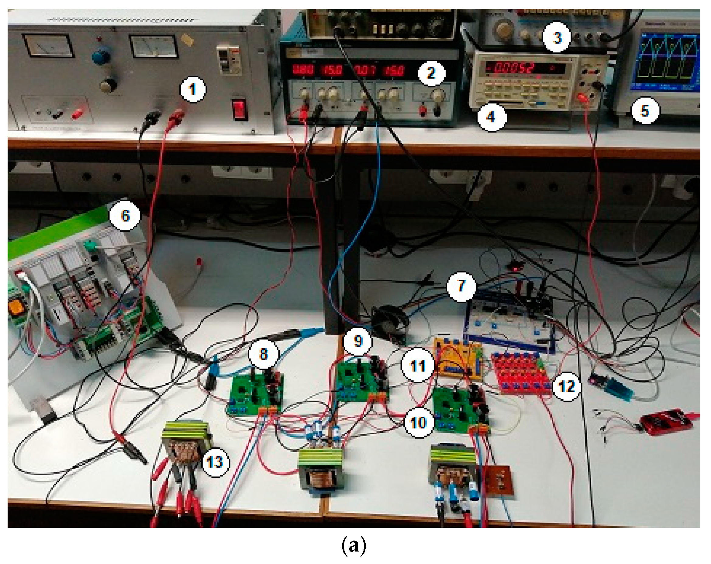
6. Experimental Results

This section is dedicated to presenting some experimental results that were obtained using a laboratorial prototype of the proposed SPV simulator. Some details of this prototype can be seen in Figure 12. Figure 12a shows a general overview of the prototype, where is possible to see three buck–boost DC–DC converters; each green PCB (printed circuit board) includes two power devices (C2M0080120D SiC MOSFET) and respective drive circuits, three inductors, a red PCB with current sensors, a yellow PCB with voltage sensors, a PLC AXC1050-PN (Phoenix Contact), and a Microchip DSP microcontroller 30F4012. To supply the system, a laboratorial DC power supply adjusted to 60VDC was used. The values of the passive components of the DC–DC converters are C1 = C2 = 470 µF, L = 1 mH. Figure 12b shows in detail the DC–DC power converter and the inductor adopted.
The components and circuits used in the laboratory prototype to perform the experimental tests are described in Table 4.
The following figure presents the diagram of the proposed buck–boost DC–DC converter on the PCB (printed circuit board) design using the Kicad software (see Figure 13a) and the respective isolated drive circuit using the UCC21520DW chip (see Figure 13b). In the proposed project, the current and voltage sensors were not introduced in the PCB of the DC–DC circuit. These devices are placed in other multipurpose boards to be applied in different projects whenever necessary. Figure 13c shows the red PCB with five current sensors (ACHS7122) with multiple adjustments (gains and offsets) and the yellow PCB with three voltage sensors (AMC1100) also with multiple adjustments (gains and offsets).
The first experimental tests were carried out to evaluate the operation of the buck–boost DC–DC power converter associated with the SPV simulator and the DSP microcontroller to accomplish the current–voltage characteristic curves (mode I). Those results can be seen in Figure 14. Figure 14a shows the output voltage (Ch1–7.5 V/div) and output current (Ch2–0.6 A/div) of the buck–boost DC–DC converter considering a continuous load variation. As this automatic test takes some time to complete using step load variations, it was connected to a multi-turn variable load available in the laboratory to perform a quick test to record the waveforms with the oscilloscope. The operator manually turns several resistors in parallel to perform the load variation. In this figure, it is possible to see the voltage variation as the current increases considering the parameters introduced by the operator (see Figure 14a), G = 1000 W/m2 at T = 25 °C. Figure 14b shows a similar result considering a continuous load variation and a solar irradiation step from G = 600 W/m2 to G = 1000 W/m2 at T = 25 °C. To conclude about the current–voltage characteristic curves and their proximity to real operation, the developed SCADA software records several data points from each test. Figure 14c,d shows the average data points of the I-V and P-V characteristic curves achieved during a practical test considering G = 1000 W/m2 at T = 25 °C. These results exhibit similar characteristics curves indicating a good approximation of the SPV panel model (one diode model), parameters, and dynamics of the DSP microcontroller. The experimental results revealed that, above a certain current value, it becomes difficult to obtain valid voltage readings due to excessive ripple in the DC–DC converters.
Additional experimental tests were performed to evaluate the performance of the system in mode II (MPPT test mode). Two experimental results in this scenario can be seen in Figure 15. The P&O MPPT algorithm was selected and designed to continuously control the duty cycle of the buck–boost DC–DC power converter. Figure 15a presents the output power (Ch3), output voltage (Ch1–50/div), and output current (Ch2–1A/div) of the buck–boost converter. Observing Figure 15, it is possible to conclude that the solution is able to generate the same output power for different weather conditions with an acceptable response. Despite the attempt to perform a load variation, when the user attempts to increase the load, the MPPT controller reduces the output voltage, which maintains the same output power. Figure 15b shows several data points achieved during the operation of the MPPT algorithm. Observing this figure, it is also possible to see that the MPPT is able to maintain the MPP (maximum power point) around the expected value despite some dispersion and a moderate response time.
The next figure shows the layout of the SCADA software developed to introduce the parameters of the SPV panel, temperature, and irradiation. These values are then sent to the PLC, which retains all data and sends them to the DSP microcontroller. The SCADA layout was developed in the VISU+ software from Phoenix Contact, and the same manufacturer of the PLC was adopted. The software operates in real time, and the data exchange is updated each 500 ms, the minimum value allowed by the software, in the available version. In the basic version, this software has three communication drives available (PROFINET, Modbus TCP/IP, and INTERBUS). The Modbus TCP/IP communication drive was selected to communicate with the PLC. The Modbus TCP/IP was preferred over the well-known PROFINET since this allows the SCADA solution to operate in controller (master) mode, whereas PROFINET was only available in device (slave) mode. The PLC adopted is the model AXC1050 PN from Phoenix Contact. The description of the automated tests is described next.
The operator must choose which mode (mode I or mode II) is going to execute in the SCADA layout. When mode I is selected, the operator must connect the output of the first converter (in buck mode) to the input of the third converter (also in buck mode). Then, they must connect the fixed RL load to the output of the third converter (this could also be performed using relays to connect and disconnect the converters, but in this case, it is performed manually). Next, the operator must introduce in the SCADA software all the desired parameters from the PV panel and also irradiance and temperature. The operator must define up to 15 desired load variations in the SCADA software. After these procedures, the operator starts the automated test in the SCADA software. The SCADA software sends all the information to the AXC1050 PN PLC over the Modbus TCP/IP protocol. After receiving the data, the PLC adjusts the duty cycle of the third converter to the first load variation step. Then, the PLC sends all the parameters to the DSP device, namely, the panel parameters, solar irradiance, and temperature. Finally, the DSP device, which has the SPV model programmed, updates the parameters and starts to read the output current and the voltage output of the first converter (buck converter as an SPV simulator) and, according to the model equations, updates the voltage reference of the converter which, using the control strategy, adjusts the duty cycle of the power switch of the converter. The PLC also records the output current and voltage of the first converter every second and sends these values to the SCADA program to show them in a trend chart. After a defined number of running cycles, the PLC adjusts the second load step, and all these procedures are repeated until the end of load variations. During this process, the parameters of the SPV panel, solar irradiance, and temperature cannot be changed until the end of the automated test. Nevertheless, the operator can stop the ongoing test at any moment, updating the values, and can restart a new automated test again. The SCADA system records the result of all the automated tests in the .csv format to be used in Excel. The following flowchart, presented in Figure 16, describes the automated test procedure applied to mode I.
In the case of selecting mode II, the operator must connect the output of the first converter (in buck mode) to the input of the second converter (in boost mode). Then, the output of the second converter must be connected to the input of the third converter (buck converter). Then, a fixed RL load must be connected to the output of the third converter. To summarize, all the converters must be connected in series. The main difference is such that, the operator must now select mode II and the desired MPPT algorithm in the SCADA software. The following procedures are similar to mode I, but in this case, besides the adjustment of the load step, the PLC also regulates the duty cycle (through the analogue output connected to a PWM modulator) of the second converter to achieve the MPP continuously. Notice that the DSP device is only running the SPV model, reading the current and voltage, and updating the voltage reference. This is critical to avoid delays in the process. The non-critical speed actions are performed by the PLC. The flowchart presented in Figure 17 describes this procedure to mode II.
The DSP device is programmed to run the SPV model, read the current and voltage, and update the output voltage reference. The SPV model requires the readings of previous output currents and voltage step cycles, and the result of the model equation gives the voltage reference to a DAC device, which is used as an output voltage reference to the sliding mode control loop. The DSP device is also used to communicate with the PLC, mainly receiving information to update the parameters and operation conditions. Notice that the output current and voltage of the first converter are used by the DSP device, and they are not sent by RS-232-C communication to the PLC. The PLC has individual analogue variables dedicated to reading this output current and voltage to speed up the process.
A simplified pseudocode of the PLC, DSPIC, and SCADA program can be found in Figure 18, Figure 19, Figure 20 and Figure 21, respectively.
The main variables and configuration statements of the DSP device are indicated in Table 5 and Table 6.
Figure 22 shows the layout of the SCADA software developed to introduce the parameters of the SPV, solar irradiance, and temperature.
Figure 23 shows the layout of the SCADA software developed to present and record data (voltage, current, power) obtained by the PLC during experimental tests, selecting the MPPT algorithm, load step variation, and other information.
Comparison aspects between several SPV simulators proposed in the literature are presented in Table 7. This comparison takes into account the following aspects: solution novelty regarding the SPV model; the accuracy of the proposed simulator regarding theoretical equations; the model supported by simulations and/or experimental results; the proposed solution explores a new or any MPPT algorithm; the complexity of the proposed simulator; the ability to perform and record the automated tests; the existence of any SCADA or HMI (human–machine interface), and the estimated hardware cost when available.

7. Conclusions

This paper presented the development of an SPV simulator system based on three buck–boost DC–DC converters. The proposed solution can generate automatic tests in two different modes, namely, to simulate the current–voltage and power–voltage characteristic curves of SPV panels (test panel mode or mode I) and the MPPT mode (mode II), the parameters of which can be introduced in the SCADA software. The proposed solution is flexible and can be changed and restarted according to new values introduced by the operator. The experimental results presented in this work demonstrate the effectuality and the good performance of the sliding mode control strategy employed in the DC–DC converter which simulates the SPV panel considering solar irradiation, temperature, and load variation. The experimental results also revealed that the adopted PLC is able to run the MPPT P&O algorithm, generating acceptable results despite some dispersion and moderate response times. Furthermore, experimental results revealed that above the MPP current value, it becomes difficult to obtain valid data due to excessive ripple in the DC–DC converters. Thus, the best results achieved a current ripple between 2% to 5% of the desired average current in MPP conditions. The major limitation is the maximum power of the designed DC–DC converters (up to 365 W) and also the difficulty of running complex MPPT algorithms. It is possible to conclude that the proposed solution can produce good results and could be a useful tool for the simulation of theoretical concepts about solar photovoltaic energy and automation.

Author Contributions

Conceptualization, A.C., H.L. and V.F.P.; Methodology, A.C., V.F.P., D.F. and J.F.M.; Software, H.L. and T.G.A.; Formal analysis, A.C., M.C., F.B. and P.F.; Investigation, A.C., P.G., H.L. and V.F.P.; Resources, A.C., V.F.P. and J.F.M.; Writing—original draft, A.C.; Writing—review & editing, A.C., H.L. and V.F.P.; Visualization, M.C., P.G., F.B., P.F., D.F. and T.G.A.; Supervision, A.C. and V.F.P.; Project administration, A.C. and V.F.P.; Funding acquisition, A.C. and V.F.P. All authors have read and agreed to the published version of the manuscript.

Funding

This work was funded by Instituto Politécnico de Lisboa, reference code: IPL/2021/ATS2SPV_ISEL.

Data Availability Statement

Not applicable.

Acknowledgments

The authors acknowledge Phoenix Contact Portugal under the EDUNET Partnership for supplying automation devices to this work.

Conflicts of Interest

The authors declare no conflict of interest.

References

  1. Baena-Moreno, F.M.; Rodríguez-Galán, M.; Vega, F.; Alonso-Fariñas, B.; Arenas, L.F.V.; Navarrete, B. Carbon capture and utilization technologies: A literature review and recent advances. Energy Sources Part A Recovery Util. Environ. Eff. 2019, 41, 1403–1433. [Google Scholar] [CrossRef]
  2. IEA. International Energy Agency Report. Global Energy Review. 2021. Available online: https://www.iea.org/reports/global-energy-review-2021 (accessed on 10 January 2023).
  3. Renewables 2021 Global Status Report—A Comprehensive Annual Overview of the State of Renewable Energy, REN21. 2021. Available online: https://ren21.net/gsr-2021/ (accessed on 10 January 2023).
  4. Zampirolli, F.A.; Josko, J.F.M.B.; Venero, M.L.F.; Kobayashi, G.; Fraga, F.J.; Goya Savegnago, D.H.R. An experience of automated assessment in a large-scale introduction programming course. Comput. Appl. Eng. Educ. 2021, 29, 1284–1299. [Google Scholar] [CrossRef]
  5. Osamnia, M.; Okada, H.; Berena, A.J.; Ueno, H.; Chunwijitra, S. A novel automated course generation system embedded in the online lecturing platform for higher education. Comput. Appl. Eng. Educ. 2016, 24, 586–598. [Google Scholar] [CrossRef]
  6. Basheer, S.; Saleh AlLuhaidan, A.; Mathew, R.M. A secured smart automation system for computer labs in engineering colleges using the internet of things. Comput. Appl. Eng. Educ. 2020, 29, 339–349. [Google Scholar] [CrossRef]
  7. Chinnasamy, J.; Shankar Ramesh Babu, K.; Chenniappan, M.; Rathinasamy, P. A workbench for motion control experiments using programmable automation controllers in industrial automation laboratory at Kongu Engineering College. Comput. Appl. Eng. Educ. 2018, 26, 566–576. [Google Scholar] [CrossRef]
  8. Gangwar, P.; Tripathi, R.P.; Singh, A.K. Solar photovoltaic tree: A review of designs, performance, applications, and challenges. Energy Sources Part A Recovery Util. Environ. Eff. 2021, 1–28. [Google Scholar] [CrossRef]
  9. Hishikawa, Y.; Doi, T.; Higa, M.; Yamagoe, K.; Ohshima, H.; Takenouchi, T.; Yoshita, M. Voltage-Dependent Temperature Coefficient of the I–V Curves of Crystalline Silicon Photovoltaic Modules. IEEE J. Photovolt. 2018, 8, 48–53. [Google Scholar] [CrossRef]
  10. Mann, S.; Fadel, E.; Schoenholz, S.S.; Cubuk, E.D.; Johnson, S.G.; Romano, G. ∂PV: An end-to-end differentiable solar-cell simulator. Comput. Phys. Commun. 2022, 272, 108232. [Google Scholar] [CrossRef]
  11. Khalid, M.S.; Abido, M.A. A novel and accurate photovoltaic simulator based on seven-parameter model. Electr. Power Syst. Res. 2014, 116, 243–251. [Google Scholar] [CrossRef]
  12. Ünlü, M.; Çamur, S. A simple Photovoltaic simulator based on a one-diode equivalent circuit model. In Proceedings of the 4th International Conference on Electrical and Electronic Engineering (ICEEE), Ankara, Turkey, 8–10 April 2017; pp. 33–36. [Google Scholar] [CrossRef]
  13. Shannan, N.M.A.A.; Yahaya, N.; Singh, B. Single-diode model and two-diode model of PV modules: A comparison. In Proceedings of the IEEE International Conference on Control System, Computing and Engineering, Penang, Malaysia, 29 November–1 December 2013; pp. 210–214. [Google Scholar] [CrossRef]
  14. Hosseini, H.S.M.; Keymanesh, A.A. Design and construction of photovoltaic simulator based on dual-diode model. Sol. Energy 2016, 137, 594–607. [Google Scholar] [CrossRef]
  15. Singh, B.; Singla, M.K.; Nijhawan, P. Parameter estimation of four diode solar photovoltaic cell using hybrid algorithm. Energy Sources Part A Recovery Util. Environ. Eff. 2022, 44, 4597–4613. [Google Scholar] [CrossRef]
  16. Sousa, S.; Onofre, M.; Antunes, T.; Branco, C.; Maia, J.; Rocha, J.I.; Pires, V.F. Implementation of a low-cost data acquisition board for photovoltaic arrays analysis and diagnostic. In Proceedings of the 2013 International Conference on Renewable Energy Research and Applications (ICRERA), Madrid, Spain, 20–23 October 2013; pp. 1084–1088. [Google Scholar] [CrossRef]
  17. Roncero-Clemente, C.; Romero-Cadaval, E.; Minambres, V.M.; Guerrero-Martinez, M.A.; Gallardo-Lozano, J. PV Array Emulator for Testing Commercial PV Inverters. Elektron. Ir Elektrotechnika 2013, 19, 71–75. [Google Scholar] [CrossRef] [Green Version]
  18. Bun, L.; Raison, B.; Rostaing, G.; Bacha, S.; Rumeau, A.; Labonne, A. Development of a real time photovoltaic simulator in normal and abnormal operations. In Proceedings of the IECON 2011-37th Annual Conference of the IEEE Industrial Electronics Society, Melbourne, VIC, Australia, 7–10 November 2011; pp. 867–872. [Google Scholar] [CrossRef]
  19. Kahoul, N.; Houabes, M.; Neçaibia, A. A comprehensive simulator for assessing the reliability of a photovoltaic painel peak power tracking system. Front. Energy 2015, 9, 170–179. [Google Scholar] [CrossRef]
  20. Subsingha, W. Real-time Photovoltaic Simulator Using Current Feedback Control. Energy Procedia 2016, 89, 160–169. [Google Scholar] [CrossRef] [Green Version]
  21. Tang, K.H.; Chao, K.H.; Chao, Y.W.; Chen, J.P. Design and Implementation of a Simulator for Photovoltaic Modules. Int. J. Photoenergy 2012, 6, 368931. [Google Scholar] [CrossRef] [Green Version]
  22. Qi, H.; Bi, Y.; Wu, Y. Development of a photovoltaic array simulator based on buck convertor. In Proceedings of the International Conference on Information Science Electronics and Electrical Engineering, Sapporo, Japan, 26–28 April 2014; pp. 14–17. [Google Scholar] [CrossRef]
  23. Cordeiro, A.; Foito, D.; Pires, V.F. A PV panel simulator based on a two quadrant DC/DC power converter with a sliding mode controller. In Proceedings of the International Conference on Renewable Energy Research and Applications (ICRERA), Palermo, Italy, 22–25 November 2015; pp. 928–932. [Google Scholar] [CrossRef]
  24. Zhang, W.; Kimball, J.W. DCDC Converter Based Photovoltaic Simulator with a Double Current Mode Controller. IEEE Trans. Power Electro. 2018, 33, 5860–5868. [Google Scholar] [CrossRef]
  25. Chakraborty, I.; Sekaran, S.; Pradhan, S.K. An enhanced DC-DC boost converter based stand-alone PV-Battery OFF-Grid system with voltage balancing capability for fluctuating environmental and load conditions. Energy Sources Part A Recovery Util. Environ. Eff. 2022, 44, 8247–8265. [Google Scholar] [CrossRef]
  26. Ahmad, R.; Murtaza, A.F.; Sher, H.A. Power tracking techniques for efficient operation of photovoltaic array in solar applications—A review. Renew. Sustain. Energy Rev. 2019, 101, 82–102. [Google Scholar] [CrossRef]
  27. De Brito, M.A.; Galotto, L.; Sampaio, L.P.; e Melo, G.D.A.; Canesin, C.A. Evaluation of the Main MPPT Techniques for Photovoltaic Applications. IEEE Trans. Ind. Electron. 2013, 60, 1156–1167. [Google Scholar] [CrossRef]
  28. Khodair, D.; Motahhir, S.; Mostafa, H.H.; Shaker, A.; Munim, H.A.E.; Abouelatta, M.; Saeed, A. Modeling and Simulation of Modified MPPT Techniques under Varying Operating Climatic Conditions. Energies 2023, 16, 549. [Google Scholar] [CrossRef]
  29. Abo-Khalil, A.G.; El-Sharkawy, I.I.; Radwan, A.; Memon, S. Influence of a Hybrid MPPT Technique, SA-P&O, on PV System Performance under Partial Shading Conditions. Energies 2023, 16, 577. [Google Scholar] [CrossRef]
  30. Asif, R.M.; Siddique, M.A.; Rehman, A.U.; Sadiq, M.T.; Asad, A. Modified Fuzzy Logic MPPT for PV System under Severe Climatic Profiles. Pak. J. Eng. Technol. 2021, 4, 49–55. [Google Scholar] [CrossRef]
  31. Siddique, M.A.B.; Khan, M.A.; Asad, A.; Rehman, A.U.; Asif, R.M.; Rehman, S.U. Maximum Power Point Tracking with Modified Incremental Conductance Technique in Grid-Connected PV Array. In Proceedings of the 2020 5th International Conference on Innovative Technologies in Intelligent Systems and Industrial Applications (CITISIA), Sydney, Australia, 25–27 November 2020; pp. 1–6. [Google Scholar] [CrossRef]
  32. Erickson, R.W.; Maksimovic, D. Fundamentals of Power Electronics, 2nd ed.; Springer: Berlin/Heidelberg, Germany, 2001; ISBN 978-0792372707. [Google Scholar]
  33. Available online: https://www.pvxchange.com/Solar-Modules/JA-Solar/JAM60S21-365-MR_1-996000354 (accessed on 10 January 2023).
  34. Asif, R.M.; Ur Rehman, A.; Ur Rehman, S.; Arshad, J.; Hamid, J.; Tariq Sadiq, M.; Tahir, S. Design and analysis of robust fuzzy logic maximum power point tracking based isolated photovoltaic energy system. Eng. Rep. 2020, 2, e12234. [Google Scholar] [CrossRef]
  35. Soon, J.J.; Low, K.S. Optimizing Photovoltaic Model for Different Cell Technologies Using a Generalized Multidimension Diode Model. IEEE Trans. Ind. Electron. 2015, 62, 6371–6380. [Google Scholar] [CrossRef]
  36. Gao, W.; Hung, J.C. Variable structure control of nonlinear systems: A new approach. IEEE Trans. Ind. Electron. 1993, 40, 45–55. [Google Scholar] [CrossRef]
  37. Silva, J.F.; Pinto, S.F. Advanced Control of Switching Power Converters. In Power Electronics Handbook, 4th ed.; Rashid, H.M., Ed.; Butterworth-Heinemann: Oxford, UK, 2018; Chapter 35; ISBN 978-0128114070. [Google Scholar]
  38. Ang, S.; Oliva, A.; Griffiths, G.; Harrison, R. Power-Switching Converters, 3rd ed.; CRC Press, Taylor & Francis Group: New York, NY, USA, 2011; ISBN 978-1439815335. [Google Scholar]
  39. Pires, V.F.; Martins, J.F.; Hao, C. Dual-Inverter for Grid Connected Photovoltaic System: Modelling and Sliding Mode Control. Sol. Energy 2012, 86, 2106–2115. [Google Scholar] [CrossRef]
  40. Mérida, J.; Aguilar, L.T.; Dávila, J. Analysis and synthesis of sliding mode control for large scale variable speed wind turbine for power optimization. Renew. Energy 2014, 71, 715–728. [Google Scholar] [CrossRef]
  41. Pires, V.F.; Silva, J.F. Teaching nonlinear modeling, simulation, and control of electronic power converters using MATLAB/SIMULINK. IEEE Trans. Educ. 2002, 45, 253–261. [Google Scholar] [CrossRef] [Green Version]
  42. PVSYST. 2022. Available online: https://www.pvsyst.com/ (accessed on 10 January 2023).
  43. Pvxchange. 2022. Available online: https://www.pvxchange.com/Solar-Modules/Schott-Solar/ASE-100-GT-FT-100W_1-992500269-1 (accessed on 10 January 2023).
Figure 1. Description of the functionality of each DC–DC converter. Despite the same topology and components, each one will perform a different function.
Designs 07 00036 g001
Figure 2. General block diagram of test panel mode (mode I).
Designs 07 00036 g002
Figure 3. General block diagram of the MPPT test mode (mode II).
Designs 07 00036 g003
Figure 4. Classic buck–boost DC–DC topology adopted; (a,b) Boost mode connection; (c,d) Buck mode connection.
Designs 07 00036 g004
Figure 5. Electric equivalent circuit of an SPV module using the single diode model.
Designs 07 00036 g005
Figure 6. Example of parameters available in the PVsyst software database [43] obtained online. Model ASE-100-GT-FT.
Designs 07 00036 g006
Figure 7. Simulation results of the characteristic curves for SPV model ASE-100-GT-FT considering different irradiations and operating temperatures: (a,b) I-V characteristic; (c,d) P-V characteristic.
Designs 07 00036 g007
Figure 8. Matlab/Simulink model of the proposed SPV simulator using the buck converter to simulate mode I.
Designs 07 00036 g008
Figure 9. Simulation results considering the system operating in mode I (test panel mode): (a) continuous load variation with output current increasing; (b) output voltage variation with load variation considering a fixed G = 1000 W/m2 and TS = 25 °C; (c) output voltage variation with load variation initial with G = 600 W/m2 and step to G = 1000 W/m2 at t = 0.5 s.
Designs 07 00036 g009
Figure 10. Matlab/Simulink model of the proposed simulator to test mode II.
Designs 07 00036 g010
Figure 11. Simulation results considering the system operating in mode II (MPPT test mode): (a) output power, (b) output voltage, and (c) output current of the boost converter controlled using the perturb and observe (P&O) MPPT algorithm.
Designs 07 00036 g011
Figure 12. Experimental setup of the proposed system; (a) general overview of the prototype, 1—DC power source, 2—power source to supply control circuit, 3—signal generator, 4—multimeter, 5—oscilloscope, 6—PLC AXC1050 controller from Phoenix Contact, 7—microchip DSP microcontroller 30F4012, 8—first DC–DC converter, 9—second DC–DC converter, 10—third DC–DC converter; 11—voltage sensor PCB, 12—current sensor PCB, 13—inductors; (b) detail of the DC–DC power converter and inductor adopted.
Designs 07 00036 g012aDesigns 07 00036 g012b
Figure 13. (a) Diagram of the proposed buck–boost DC–DC converter on the PCB (printed circuit board) design using the Kicad software; (b) Isolated drive circuit using the UCC21520DW chip placed in the DC–DC board; (c) Photographs of the PCBs with current sensors (five ACHS7122), red PCB and voltage sensors (three AMC1100), yellow PCB.
Designs 07 00036 g013
Figure 14. Experimental result in test panel mode (mode I): (a) output voltage (Ch1–7.5 V/div) and output current (Ch3–0.6 A/div) during a continuous load variation; (b) Similar to (a) considering a step solar irradiation from G = 600 W/m2 to G = 1000 W/m2 both at T = 25 °C; (c) average data points recorded by the SCADA software for the I-V characteristic curves, at G = 1000 W/m2 and T = 25 °C; (d) Similar to (c) applied to P-V characteristic curves.
Designs 07 00036 g014
Figure 15. Experimental result in mode II (MPPT test mode): (a) output power (Ch3), output voltage (Ch1–50/div) and output current (Ch2–1A/div) of the boost converter considering two-step load variations; (b) multiple data points achieved during the operation of the P&O MPPT algorithm.
Designs 07 00036 g015
Figure 16. Flowchart of the automated test procedure applied to mode I.
Designs 07 00036 g016
Figure 17. Flowchart of the automated test procedure applied to mode II.
Designs 07 00036 g017
Figure 18. Simplified pseudocode of the main PLC task (developed in Structured Test according to IEC61131-3).
Designs 07 00036 g018
Figure 19. Simplified pseudocode of the perturb and observe MPPT algorithm running in the PLC (developed in Structured Test-IEC61131-3).
Designs 07 00036 g019
Figure 20. Simplified pseudocode of the DSP device programmed in C code.
Designs 07 00036 g020
Figure 21. Simplified pseudocode of the main window of SCADA software in C code.
Designs 07 00036 g021
Figure 22. SCADA software layout developed to introduce parameters of the SPV panel, including temperature and irradiation.
Designs 07 00036 g022
Figure 23. SCADA software layout developed to present and record data (voltage (green line), current (red line), power (blue line)) obtained by the PLC during experimental tests.
Designs 07 00036 g023
Table 1. Summary of the different operation modes and converter’s functionality.
Operation ModeConverter UsedTopologyDescription
Mode I (SPV panel mode)1st converter connected in series with…Buck modeSimulate the I-V PV curves
3rd converterBuck modeSimulate a variable load
(Fixed load with variable voltage)
Mode II (MPPT test mode)1st converter connected in series with…Buck modeSimulate the I-V PV characteristics
2nd converter connected in series with…Boost modeSimulate the MPPT
algorithm
3rd converterBuck modeSimulate a variable load
(Fixed load with variable voltage)
Table 2. Characteristics of an SPV panel with the maximum power of the proposed converter (in STC) [32].
ParameterValue
Voltage at MPP33.6 V
Current at MPP10.75 A
Power at MPP365 W
Open-circuit voltage41.13 V
Short-circuit current11.3 A
Table 3. Components selected for the DC–DC converters used in the simulations.
ParameterValue
InductorsL = 1 mH
CapacitorsC1 = C2 = 470 μF
Input Voltage (first converter)VDC = 60 V
Voltage at MPP34.2 V
Current at MPP2.98 A
Power at MPP10.8 W
Open-circuit voltage42.2 V
Short-circuit current3.22 A
Equivalent shunt resistor400 Ω
Equivalent series resistor1.32 Ω
Power switchesRon = 10−3
DiodesRon = 10−3 Ω; Vf = 0.8V
Load (last converter)R = 100 Ω; L = 0.5 mH;
Table 4. Components and circuits used in the laboratory prototype.
Component or CircuitValue
InductorsL = 1 mH (manually created)
CapacitorsEPCOS–C1 = C2 = 470 μF, 200 V
Power DevicesC2M0080120D SiC MOSFET (1200 V; 36 A) with freewheel diode
Filtering capacitors2.2 μF, 400 V
Isolated drive circuitsTI–UCC21520DW
Auxiliary Isolated power sourcesMurata–NMA1215SC
Main Power SourceWanptek–100VDC; 20 A.
DSP deviceMicrochip DSPIC30F4012
DAC deviceMicrochip 12-bits MCP4922
PLCPhoenix Contact–ACX-1050-PN
Current sensorsACHS7122; Current range: ±20A; Sensitivity: 100 mV/A; Primary conductor resistance: 0.7 mΩ; Bandwidth: 80 kHz; Total output error of ±1.5%
Voltage sensorsAMC1100; ±250 mV input voltage range optimized for shunt resistors; Offset error: 1.5 mV; Input bandwidth: 60 kHz min; Fixed gain: 8 (0.5% Accuracy).
Table 5. Configuration statements of the DSP device.
Configuration StatementsValue
%Oscillator
    #pragma config FPR FRC_PLL16 %Primary Oscillator Mode (FRC
    #pragma config FOS PRI %Oscillator Source (Primary Oscillator)
    #pragma config FCKSMENCSW_FSCM_OFF %Clock Switching and Monitor
%Watchdog
    #pragma config FWPSBWDTPSB_16 %WDT Prescaler B (1:16)
    #pragma config FWPSAWDTPSA_512 %WDT Prescaler A (1:512)
    #pragma config WDT WDT_OFF %Watchdog Timer (Disabled)
%Voltage Protection
    #pragma config FPWRTPWRT_64 %POR Timer Value (64 ms)
    #pragma config BODENV BORV42 %Brown Out Voltage (4.2 V)
    #pragma config BORENPBOR_ON %PBOR Enable (Enabled)
    #pragma config MCLRE MCLR_EN % Master Clear Enable (Enabled)
%Code protection
    #pragma config GWRP GWRP_OFF %General Code Segment Write Protect
    #pragma config GCP CODE_PROT_OFF %General Segment Code Protection
%Programming
    #pragma config ICS ICS_PGD %Comm Channel Select (Use PGC/EMUC)
Table 6. Declaration Variables of the DSP device.
TypeVariable
floatVT
floatn
floatVOC_STC
floatISC_STC
floatIO
floatRS
floatRT
floatVOC
floatISC
floatKi
floatKv
floatdT
floatT
floatG
floatNcell
floatVPVref
floatVPV
floatVPVref5V
floatIPV
integerVPVrefWord
integerDataReceived = 0
charbuffer (80)
charrxbuffer (80)
charrxbuffer2 (80)
Table 7. Comparison between SPV simulators proposed in the literature.
CharacteristicsSolution
[11][12][14][15][16][17][18][19][20][21][22][23]Proposed
New SPV modelYesNoNoYesNoNoNoNoNoNoNoNoNo
Model AccuracyGoodMed.GoodGoodLowMed.Med.Med.Med.Med.LowMed.medium
Simulations resultsYesYesYesYesYesNoNoNoYesYesYesYesYes
Experimental resultsNoYesYesNoYesYesYesYesNoYesYesYesYes
Hardware developedNoNoYesNoYesYesNoYesNoYesYesYesYes
New MPPT algorithmNoNoNoNoNoNoNoNoNoNoNoNoNo
Any MPPT algorithm
included
NoNoNoNoNoNoNoYesNoNoNoNoYes
Complexity
implementation
Med.LowLowMed.LowMed.LowLowLowLowLowLowMed.
Automated testsNoNoYesNoNoNoYesYesNoNoNoNoYes
SCADA/HMI
interface
NoNoYesNoYesNoYesNoNoNoNoNoYes
Hardware Cost*NALowHigh*NALowHighHighLow*NALowLowLowLow
*NA—not applicable.
Disclaimer/Publisher’s Note: The statements, opinions and data contained in all publications are solely those of the individual author(s) and contributor(s) and not of MDPI and/or the editor(s). MDPI and/or the editor(s) disclaim responsibility for any injury to people or property resulting from any ideas, methods, instructions or products referred to in the content.

