Article

A Predesign Methodology for Power Electronics Based on Optimization and Continuous Models: Application to an Interleaved Buck Converter

1
CEA, LITEN, DEHT, LAEH, Université Grenoble Alpes, F-38000 Grenoble, France
2
Power Electronics Lab, Bern University of Applied Science, 2501 Biel, Switzerland
3
CNRS, Grenoble INP, G2Elab, Université Grenoble Alpes, F-38000 Grenoble, France
4
Schneider Electric, Eybens, F-38000 Grenoble, France
*
Author to whom correspondence should be addressed.
Designs 2022, 6(4), 68; https://doi.org/10.3390/designs6040068
Submission received: 30 June 2022 / Revised: 24 July 2022 / Accepted: 1 August 2022 / Published: 3 August 2022
(This article belongs to the Section Energy System Design)

Abstract

:
This paper proposes an approach dedicated to power electronics preliminary design. It consists in setting the optimization problem in an “imaginary” world by considering all decision variables to be continuous. The method is illustrated in detail with the real case study of an Interleaved Buck Converter. The models used are briefly described, and the focus is also placed on all possible applications of such a quick design methodology: considering several operating points, checking various candidate technologies and negotiating the specifications of the converter with the partners.

1. Introduction

During the preliminary design stage, power electronics designers must quickly negotiate the converters specifications with the system integrator or partners. Generally, some back-of-the-envelope calculations are sufficient. However, in some cases, the system is so much constrained that only optimization methods can provide satisfying results as quickly as needed. The converter requirements are often contradictory: for example, minimizing the converter current ripple and, at the same time, its weight. The challenge is therefore not only selecting some components in the database, but finding the right trade-off between all end-user criteria. This challenge is repeated each time a new project is started [1]; therefore, an effective methodology is required.
In addition to technical objectives and constraints, the designers have to deal with the design process paradox [2] and the development expenditure [3]. Indeed, it is during the preliminary design phase that the system specifications and development plan are defined. At this stage of the project, the knowledge about the system to design is low, while the degree of freedom to influence the development cost is high (Figure 1). The approach must be able to handle undefined or fluid requirements, as well as a large degrees of freedom, in a very short time.
In power electronics, if there are usually only few components to be selected for a dedicated topology, the choice among them is wide. There are therefore a combinatory set of possible solutions. Exploring each of them to define if the components or system requirements are fulfilled and then defining the best ones according to a criterion is a complex (optimization) problem to be solved.
There are three main families of optimization methods to solve this kind of problem: the heuristic, the mathematic and the metaheuristic [4].
For example, with a heuristic method, the designers may use general design rules and several hypotheses (such as limiting the inductor current ripple to 20% in the inductor to limit iron losses). This technique allows pre-sizing the converter quickly by decreasing the number of possibilities, but presents the risk of leading to sub-optimal products. Another possibility is to use combinatory exploration, but the size of the optimization problem must be limited.
The metaheuristics method, such as stochastic optimization, is able to find the global optimum and able to optimize the system with discrete parameters (such as component choice among manufacturer catalogs) [5,6,7]. Nevertheless, they are also limited in the number of handled constraints and design variables. However, when observing the optimization results of the stochastic optimization of a DC-DC converter as in Figure 2 from [5], its discrete Pareto front actually looks almost continuous.
So, if the system could be represented with only continuous variables, then it would be possible to use mathematic optimization algorithms. In [8], a very powerful algorithm was used, using geometric programing. However, this method requires that all models are expressed as posynomial functions, which is not easy for every constraint of power electronics. For instance, power quality as THD (Total Harmonic Distortion) or EMC (ElectroMagnetic Compatibility) requires quite complex models to be accurate enough. Therefore, in this paper, the choice was made to use Sequential Quadratic Programming, which is efficient with large optimization problems and only requires the differentiability of the models, allowing more freedom on the model formulation. This is the new approach proposed in this paper: pre-size by optimization of power electronics systems with design variables considered as continuous in an “imaginary” world (i.e., not limited to existing devices or topologies).
Section 2 details this new approach. Section 3 introduces a concrete study case for the proposed methodology, with the preliminary design of an Interleaved Buck Converter (IBC) for an innovative airship named Stratobus [9,10]. It is shown that the formulation of the optimization problem is a major step of the method that is detailed in Section 4. Section 5 briefly describes how a designer can build a continuous model of a converter, each proposal being illustrated with the study case. Then, Section 6 shows the interest of optimizing in the imaginary world, also by negotiating the set of specifications of the IBC (Section 7). Finally, a discretization process is proposed to come with the pre-sizing of a manufacturable converter in Section 8. Even if the results of this paper are illustrated using the specific case of an Interleaved Buck Converter (IBC), many models presented here can be developed in a similar way for other power electronics topologies. he semiconductor loss models (based on analytical description of switch and conduction stages) and capacitor models (based on datasheet interpolation) are very generic. Inductor loss model is also representative of many power electronics structures, even if more accurate models can be used [11], and even saturation effect taken into account [12]. The thermal model of the inductor is limited to molded devices, since only conduction is considered, but it offers an idea on how other models could be built, depending on the technology. Frequency models for THD use a representation in the frequency domain based on equivalent sources and transfer function, which can apply to various topologies. The aim of this paper is not only to illustrate the detailed process for running a design by optimization in a continuous “imaginary” world, as also described in other papers [8,12], but also to illustrate all the possibilities offered by this kind of methodology in a preliminary design step (Section 6, Section 7 and Section 8). In particular, it shows that considering several operating points together, negotiating the various constraints and investigating various technologies can be conducted very easily and quickly, when the problem is formulated properly.

2. Proposed Approach for Preliminary Design

2.1. Presentation of the Design Method

The proposed approach intends to keep a high degree of freedom and explore a wide range of possibilities by optimizing the system in a continuous “imaginary” world where all discrete variables are assumed continuous (keeping physical laws still valid).
In power electronics, the discrete variables can be split in three categories:
  • The discretized variables (D): variables that are physically continuous but industrially discretized, such as a set of capacitors references.
  • The natural number variables (N): variables of the system that are constrained to natural numbers for practical reasons (number of levels of a multi-level converter, turn number of an inductor, etc.)
  • The technology or topology choice variables (T): variables that only have distinct values (such as topology choice between buck or boost, or technology choice: SiC vs. Si, magnetic material).
All discretized variables (D) can be handled as continuous since the physics behind is not changed. In some cases, a natural number (N) can be replaced by real numbers because it does not modify significantly the physical behavior. For instance, the turn number in an inductor. In other cases, a specific formulation of the problem has to be written so that the natural number can be replaced by a real number. This is briefly illustrated in Section 5.1.2. (and is detailed in [13]). The last case of Technology/Topology case (T) has to be handled on a case-by-case basis.
One statement and one assumption are used for the proposed approach:
  • Statement: if there are no solutions in the imaginary (continuous) world, then there are no solutions in the real (discrete) world.
  • Assumption: the performances of the imaginary solutions are very similar to the performances of the locally discretized solutions.
The advantage of the imaginary world is therefore to be a kind of “theoretical optimum”, suitable to quickly evaluate the impact of the specifications or of technological choices.

2.2. The Different Stages of the Proposed Method

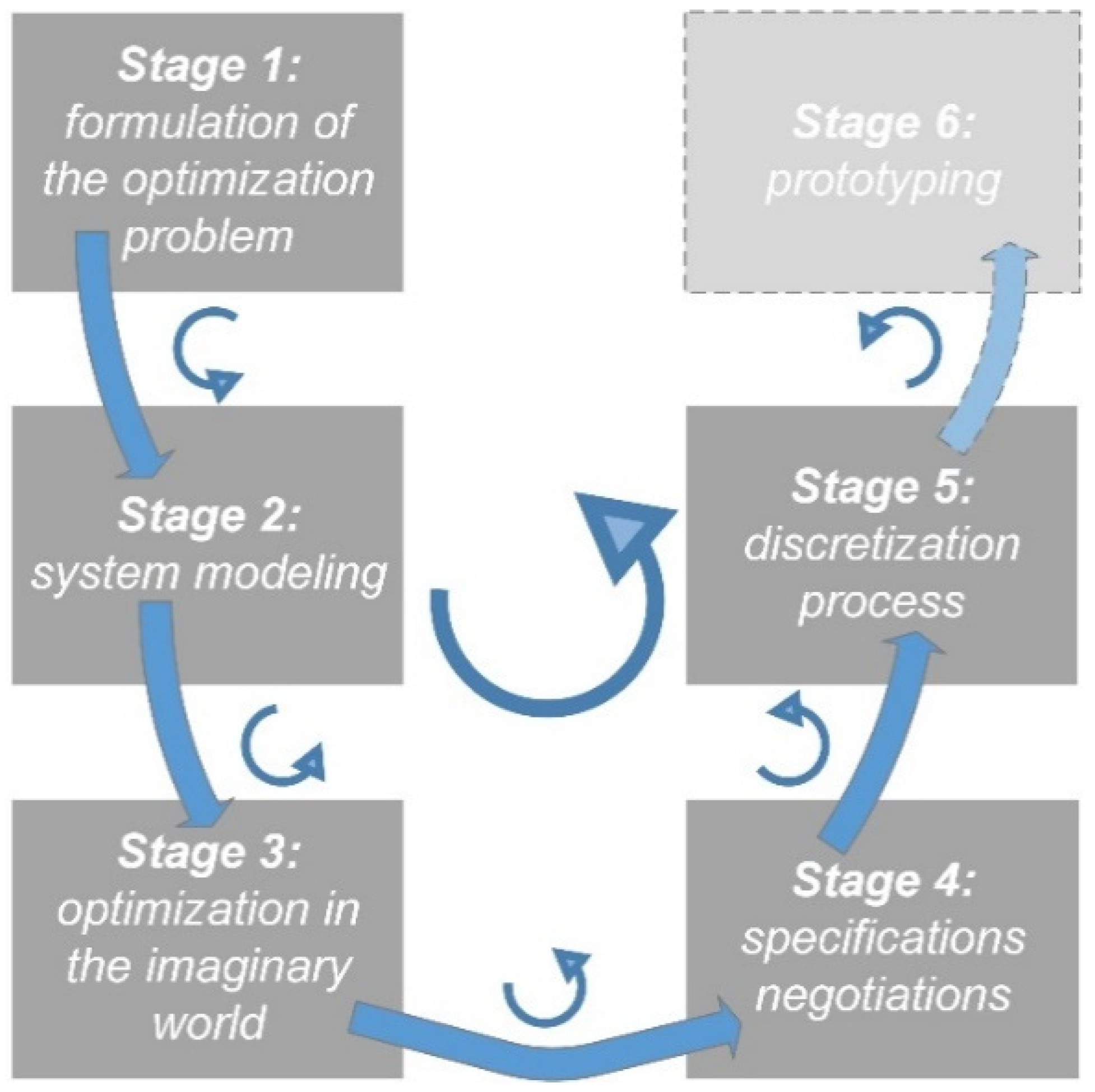
The different stages of the proposed process are illustrated in Figure 3.
Stage 1 (formulation of the optimization problem) is the definition of the design method and the input, objectives and constraints variables.
Stage 2 (system modeling) is dedicated to the creation of the models of the system and its sub-systems with only continuous variables.
Stage 3 (optimization in the imaginary world) is used to confront the optimization model (with only continuous variables) to the optimization problem with an initial (preliminary) set of specifications of the product.
Stage 4 (specifications negotiations) is the reason of the proposed approach. During this stage, the designer makes several parametric optimizations and Pareto front to negotiate the product requirements.
Stage 5 (discretization process) is when the designer must come back in the real world (with discrete variables) from the optimal imaginary solution of the negotiated set of specifications.
Stage 6 (prototyping) is the time where the first prototype is designed and tested (as in a classical process).
It is worth noting that, between each step, some feedback can be made in order to improve the model formulation or the model quality, which makes this process iterative.

3. Study Case

3.1. Context

Stratobus is a concept leaded by Thalès Alenia Space [10]. It is an electrical airship and it will be set in the Stratosphere for communication and surveillance missions.
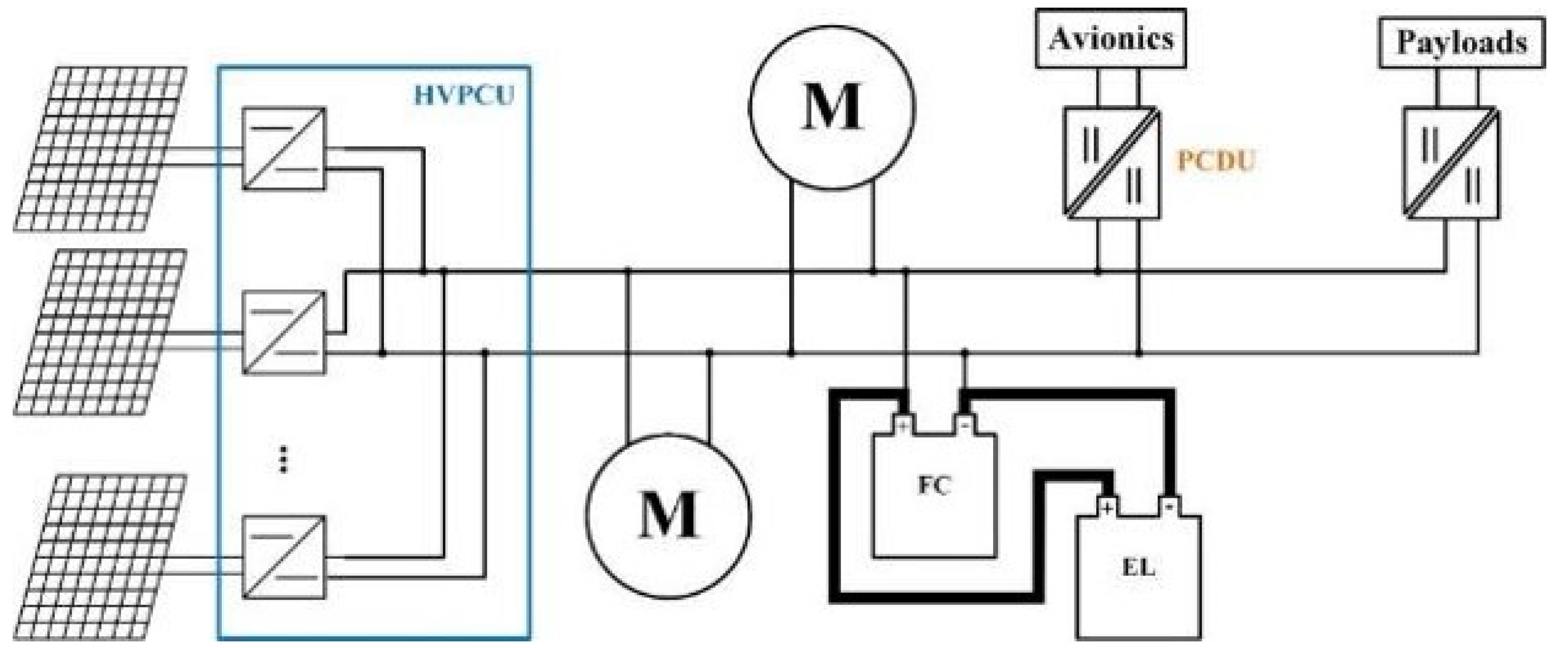
During the day, solar panels provide the necessary energy to the airship (avionic systems, motors and payloads) and to an electrolyze unit that produces hydrogen. During the night, a fuel cell takes over the solar panels. Figure 4 shows the electrical architecture of Stratobus.
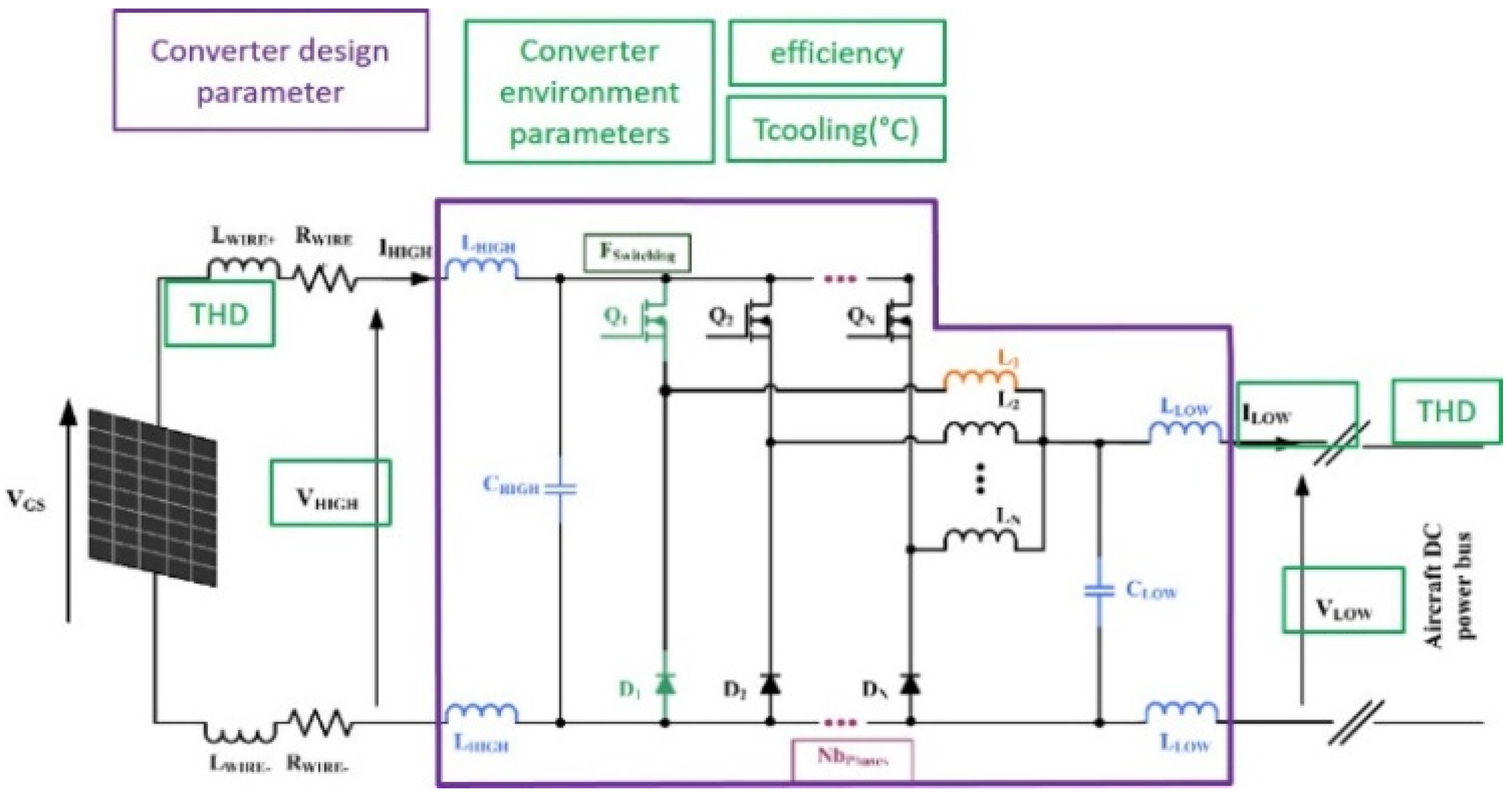
The exact voltages and power values indicated on Figure 5 and Table 1 were changed for confidentiality reasons, but are of the same order of magnitude. Additionally, these values were subjected to several changes during the preliminary design phase. The system integrator (Thales) has indeed to define the best trade-offs to minimize the airship weight. One of the numerous questions was, for example: “Is it lighter to have higher or lower voltage solar panels?” Indeed, the solar panels maximum output voltage affects the weight of cables, but also the weight of the DC-DC converters.
Each change in the global architecture influences the sub-systems design. The system integrator must know how much these changes influence the sub-systems power density in a short, dedicated time. That is one of the reasons of the need of a dedicated design methodology. This paper focuses on the preliminary design method illustrated with the DC-DC converters between the solar panels and the DC electrical bus.

3.2. DC-DC Converter Study

Table 1 provides a preliminary set of specifications for the DC-DC converter.
Table 1. Converter preliminary specifications.
CriteriaMinimum ValueMaximum Value
Power density7 kW/kg is a must10 kW/kg nice to have
Input power 0 W4.5 kW/5 kW for peak value
Input voltage 450 V800 V
Output voltage 200 V430 V
Efficiency96%NA
Input/Output current THDNA5%
Cooling temperature−40 °C65 °C
Ambient temperatureTBD85 °C
Ambient pressure0.07 bar1 bar
The selected topology to fulfill these requirements is the Interleaved Buck Converter (IBC) with uncoupled phase inductors (Figure 5). The topology selection is not detailed in this paper, since it is not the core topic of the paper.
The filtering inductors can be associated in series/parallel and the capacitors can be paralleled. The conduction mode (either continuous or discontinuous) is free, but must be the same for a wide range of the operating conditions of the converter, for control stability.

4. Formulation of the Optimization Problem for Pre-Sizing in the Imaginary World

Designing a power converter using an optimization method necessitates, at first, formulating the design problem appropriately. This is often not straightforward for the power electronics expert: defining design variables, constraints and an objective function is the starting point of the problem, and sometimes requires a new way of thinking.
The formulation of the problem consists of:
  • Defining the problem objectives, constraints and design parameters (in other words optimization input, output and objective variables);
  • Selecting an optimization method and algorithm;
  • Setting the model of the system to be optimized (define the right organization of the sub-models).
These three steps cannot be performed independently. The following sections provide some advice to set the preliminary design problem of power electronic systems in the imaginary world. It is in particular illustrated with the study case.

4.1. Definition of the Study Case Problem Objectives, Constraints and Design Parameters

The critical criteria of all the Stratobus airship systems are the weight to be minimized. The designer of the DC-DC converter of the study case should minimize the converter weight while fulfilling its constraints. Therefore, the main design parameters, such as the number of turns of the phase inductor or semiconductors switching frequency, have to be input variables of the problem. The input design variables of the study case are listed in Table 2. Their discretization nature is superscripted to their abbreviation (D for discretized, N for Natural number and T for technology or topology choice).
The weight of each part of the converter, in addition to its global weight, has to be set as output objective of the model to minimize. The system level variables, as input/output voltage, maximum and minimum power or Total Harmonic Distortion (THD), are also to be considered as parameters, since they are subject to change during the design, in order to evaluate their impact on the objective function.
Finally, other constraints are to be considered, at component level: the maximum temperature of the devices or geometrical limitations (turn number fitting the winding area in an inductor for instance).

4.2. Selection of the Method and the Algorithm

The choice of the proper algorithm has to be made depending on the application. Because in the preliminary design phase, the number of unknown and undefined parameters is quite high, and the size of the optimization problem is relatively large. In the present case study, the operating range of the converter was also wide, which multiplies the number of constraints to be considered. Consequently, mathematic gradient-based optimization algorithm was adapted [4]. However, this algorithm has the drawback of requiring, respectively, the first and second derivatives of the model (and so continuous and differentiable model). The gradient must be very accurate to avoid false convergence or divergence of the optimization.
In this study, a homemade optimization framework was used: CADES. It automatically computes the exact gradient of the model when properly written [14] and this in a short of time [15]. Therefore, from a user point of view, no additional work is needed, except writing the equations of the model, and ensuring it is derivable.
Finally, for the study case, Sequential Quadratic Programming (SQP) first order optimization algorithm [16] was chosen.

4.3. Definition of the Model for the Proposed Approach with the Study Case

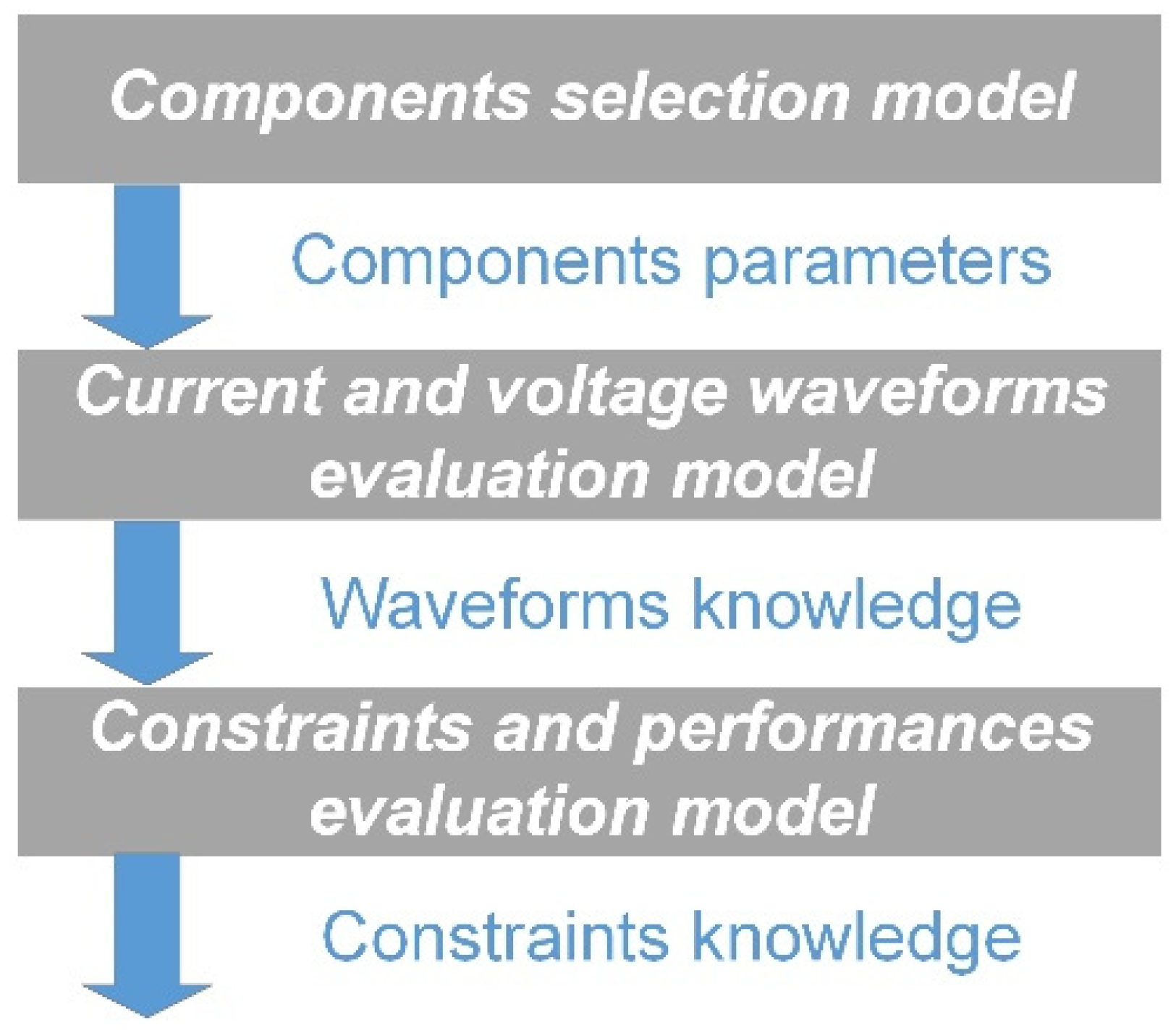
To obtain a continuous model of power electronics systems, the designer should organize the sub-models by following the physic of the system. In other words, the model of the system should be organized according to Figure 6. They are briefly illustrated in Section 5.

5. Modeling Power Electronics in the Imaginary World

This section provides some examples of continuous and derivable models suitable for power electronics systems. In the study case, the first models to be described are linked to the input and output filter of the converter in order to meet the corresponding THDs (Total Harmonic Distortion). Secondly, the phase inductor models are briefly explained. Then, the switching cell models are presented. All these analytical models were experimentally tested with a prototype.

5.1. Modeling the Filtering Function

5.1.1. Filtering Components Selection Models

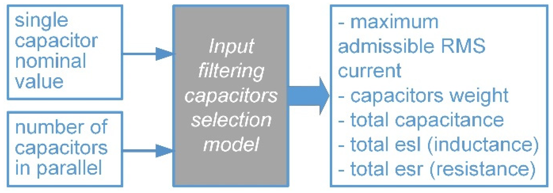
For input and output filters, it was chosen to associate “of the shells” components (contrary to phase inductor, which has to be carefully designed due to high constraints). A pre-selection of the series of capacitors and inductors among the manufacturer’s catalogs was made according to the criteria of weight and aeronautical (Stratospheric) constraints. The optimization algorithm has nevertheless the choice of the component among series and the possibility to parallelize the capacitors and associate in series/parallel the inductors. Figure 7 shows the input filtering capacitor selection model with its input and output optimization variables. The number of devices was obviously an integer, but was considered as real number in the optimization process to keep derivability.
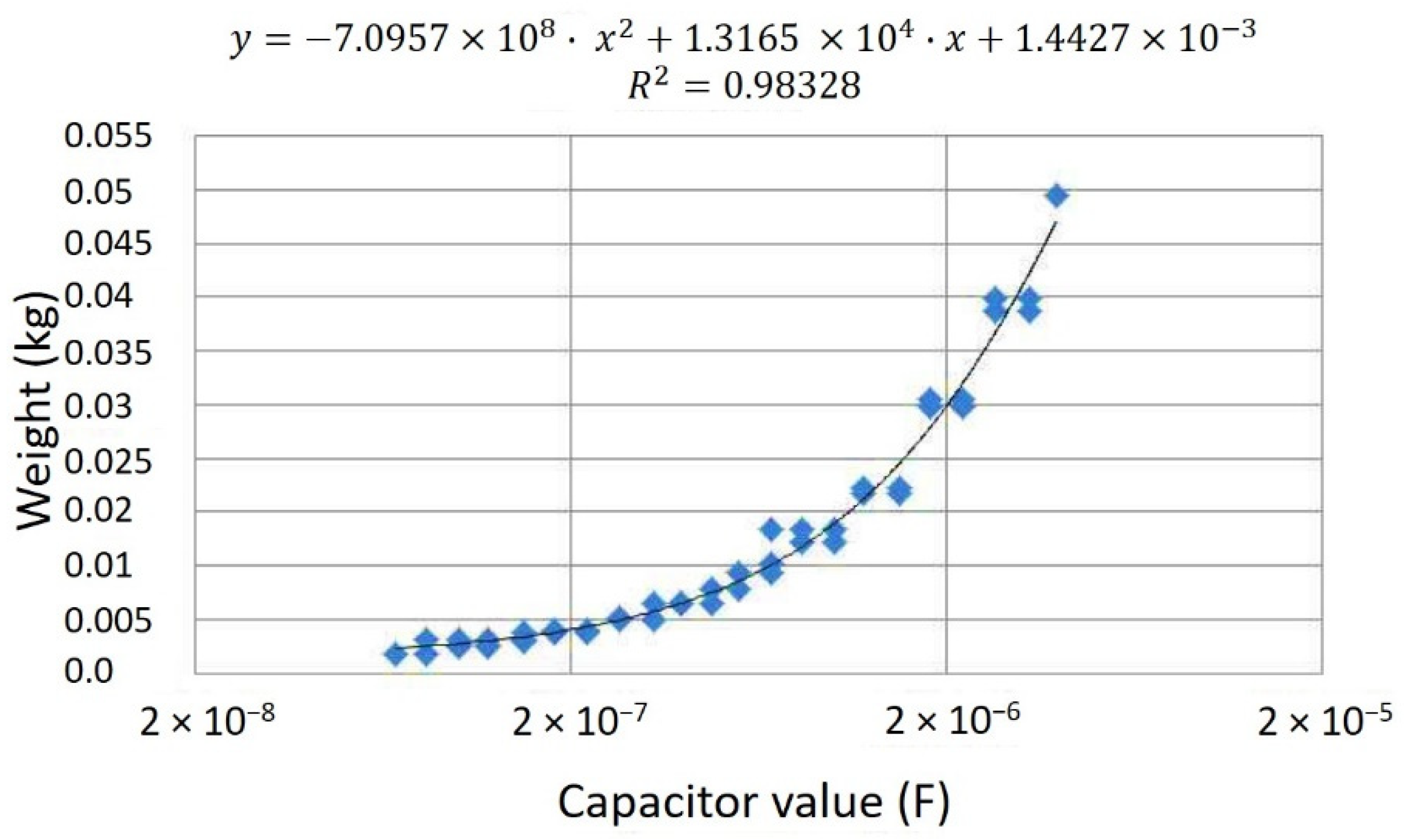
The filtering capacitors and inductors datasheet were therefore interpolated based on the model formulation of Figure 7, as in the example of Figure 8.

5.1.2. Converter Input and Output Current Switched Waveforms Evaluation Models

With interleaved Buck or Boost topologies, the input and output current ripples are linked to its number of phases [17]. In the literature, the models of current ripples of IBC are either not analytical [18], or not continuous and differentiable [19]. They are all set in the time domain.
Therefore, the problem was transferred from time to frequency domain. Expressing the current ripple in the frequency domain allows obtaining a simple dependence with the IBC number of phase [13]. From this expression, the model can become continuous and derivable, considering a non-integer number of phases. It may be quite surprising to have a non-integer number of phases, but the global behavior of the converter is captured, and this is the most important point. Coming back to real world (Stage 5 in Figure 4) is of course feasible, but not necessary when discussing the impact of the specifications on the converter performances, as it will be illustrated in Section 6.

5.1.3. Converter Input and Output Current THD Evaluation Models

Thanks to the filters transfer functions and the IBC input and output current spectra, the evaluation of the converter input and output current THD is straightforward. Additionally, the software automatically generates the filters frequency models [15]. The model derivatives computation time is kept low: the model can afford up to 20 harmonics evaluation during optimization.

5.2. Phase Inductor Modeling

The pre-selected technologies for the IBC phase inductors were powder-distributed air gap core and copper Litz wire. To reduce the stray capacitance, the number of layers was limited to one and an external constraint (connector size) limited the inductor winding current density to 5 A/mm².

5.2.1. Phase Inductor Sizing Direct Model

The geometrical data of the inductor as core dimensions, Litz strands diameter and number were considered as the input optimization variable of the inductor-sizing model. The exact material reference (chemical composition with associated properties) of the inductor core was kept as a discrete input design parameter that the optimization algorithm will not be able to modify. The designer (or an automatized script) has to perform as much optimizations as the desired number of studied core materials.
With these data and the knowledge of the global input optimization variables that are the IBC number of phases, switching frequency and output current, the evaluations of the inductance, DC resistance and weight of the phase inductor are direct.

5.2.2. Phase Inductor Constraints Evaluation

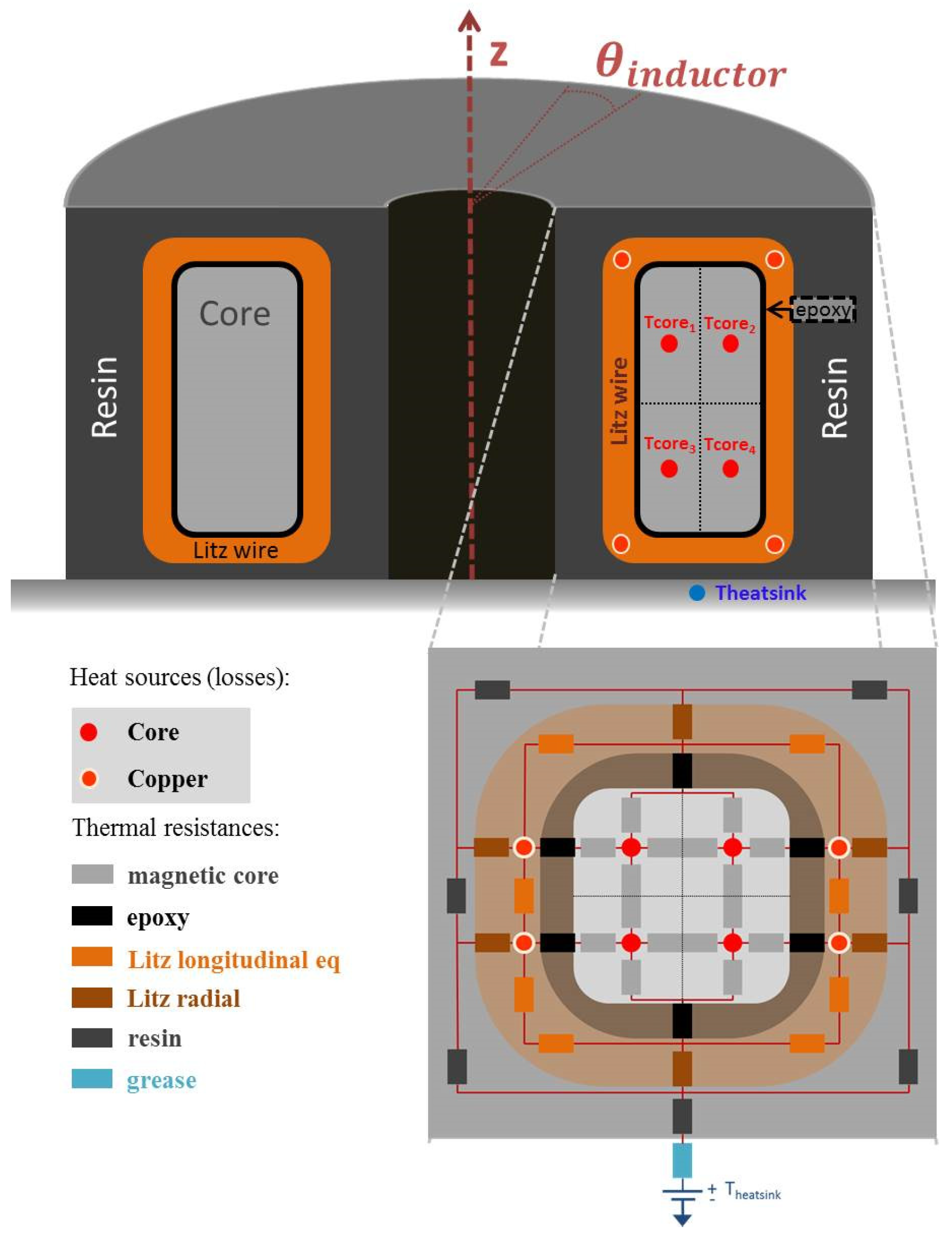
The inductor has to fulfill a maximum operating temperature. It is evaluated using both losses models and a global thermal model. For core losses, IGSE [20] was used. For winding AC and DC losses, the simple formula from [21] was chosen, even if Dowell method could have been used as in [22]. Knowing the losses, the inductor geometry and material data, a 2D thermal model [23,24] (Figure 9) helps to obtain the inductor hot point temperature, which has to stay below a certain limit.

5.3. Semiconductor Selection Model

The technology choice for the studied application was Silicon Carbide (SiC). Voltage rating was fixed at 1200 V to switch the maximum input voltage that is around 800 V. Because the IBC semiconductors RMS current depends on its number of phases, their current rating must be an input optimization variable [25,26].
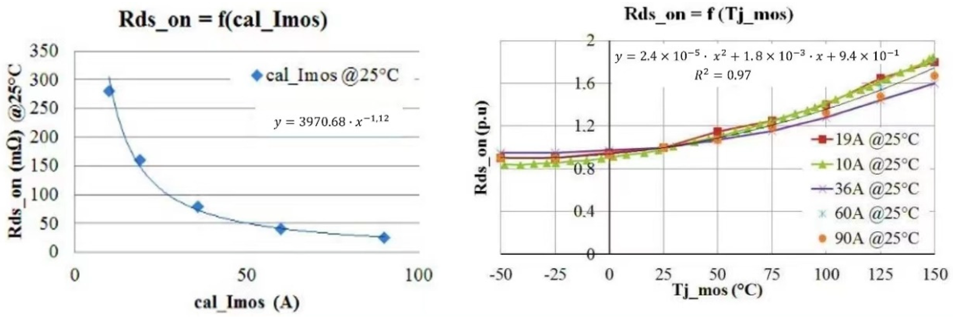
The manufacturer datasheets of 1200 V SiC MOSFET and Schottky diodes were interpolated to obtain the semiconductors electrical and thermal properties (capacitances, on-state resistances, thermal resistance, etc.), according to their current rating at 25 °C. The junction temperature was also considered thanks to corrective coefficient: Equation (1) is an example of MOSFET ON-state resistance evaluation based on Figure 10.
R d s O N = C ( I r a t i n g ) α ( k 1 T j ² + k 2 T j + k 3 )
Finally, there are two input optimization variables for each semiconductor selection model: their current rating and junction temperature.

5.3.1. Semiconductors Losses and Thermal Model

Thanks to the knowledge of semiconductors electrical and thermal properties and switched current and voltage (i.e., converter switching cell voltage and current waveforms), the classical analytical model [27] can be used to determine their conduction and switching losses. Then, a simple 1D thermal model allows determining the MOSFET and diode junction temperatures. It means that the junction temperature is both an input and output optimization variable. It is called an implicit equation to solve [28].

5.3.2. Management of the Junction Temperature Implicit Equation

This implicit equation is directly solved by the optimization algorithm in the study case. A new constraint Const_Tj is added (for model validity only) as in Equation (2), with T j o u t p u t the evaluated junction temperature and T j i n p u t the model input junction temperature.
C o n s t _ T j = T j o u t p u t T j i n p u t
This variable is constraint during the optimization to be null or very small. The optimization algorithm is therefore in charge of finding the thermal steady state of the switching cell.

5.4. Test of the Models’ Validity Domain

Since optimization explores a wide range of solutions, it is mandatory to have the knowledge of validity domain of the models. A prototype was therefore built to verify the results. In the study case, a 3-phase Interleaved Buck Converter working in Discontinuous Conduction Mode was used to review the models. The test bench is fully described in [26]. The converter global efficiency and the phase inductor losses were electrically measured, while the semiconductors losses were thermally measured after a calibration procedure.
Several operating points were tested: the converter power was swept with fixed input and output voltages, then the input voltage was swept with fixed power and output voltage and, finally, the output voltage was swept.
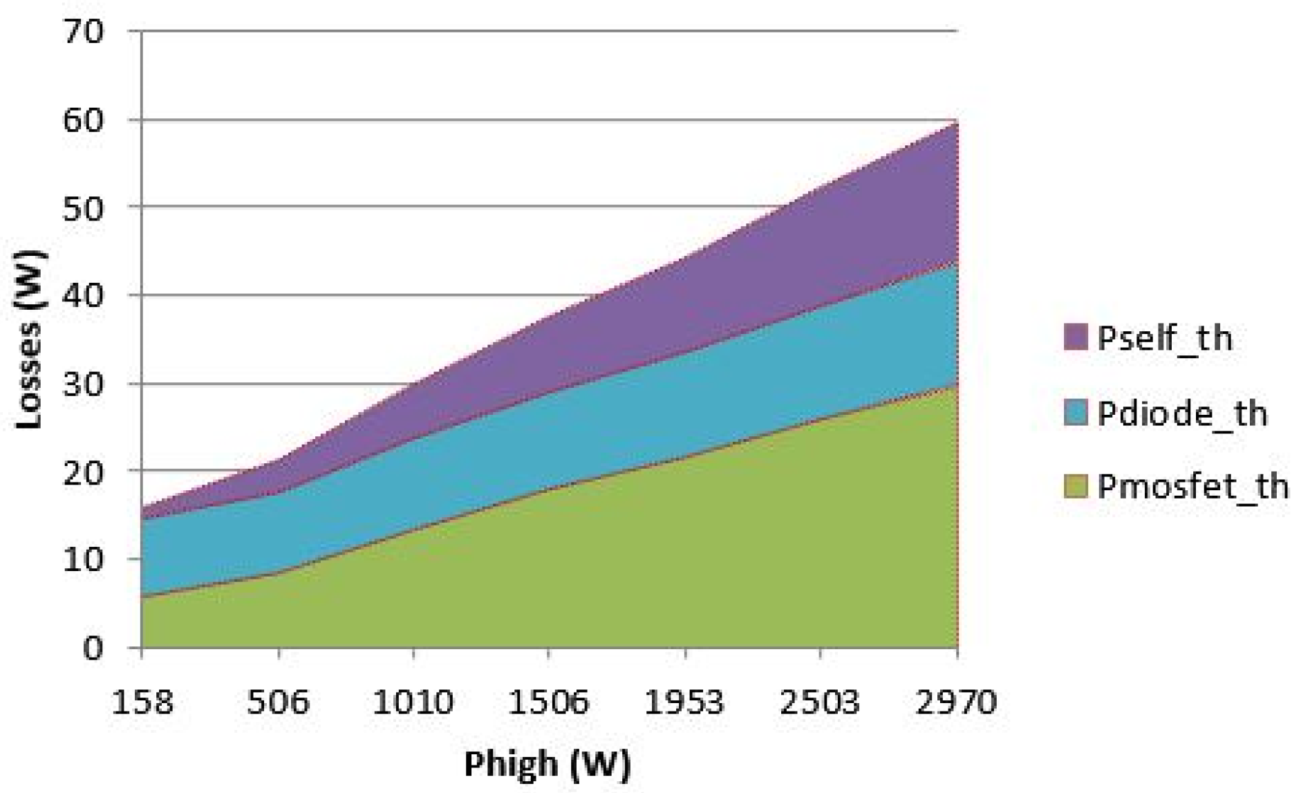
Figure 11 presents the repartition of the losses between the different power devices in the case of swept power.
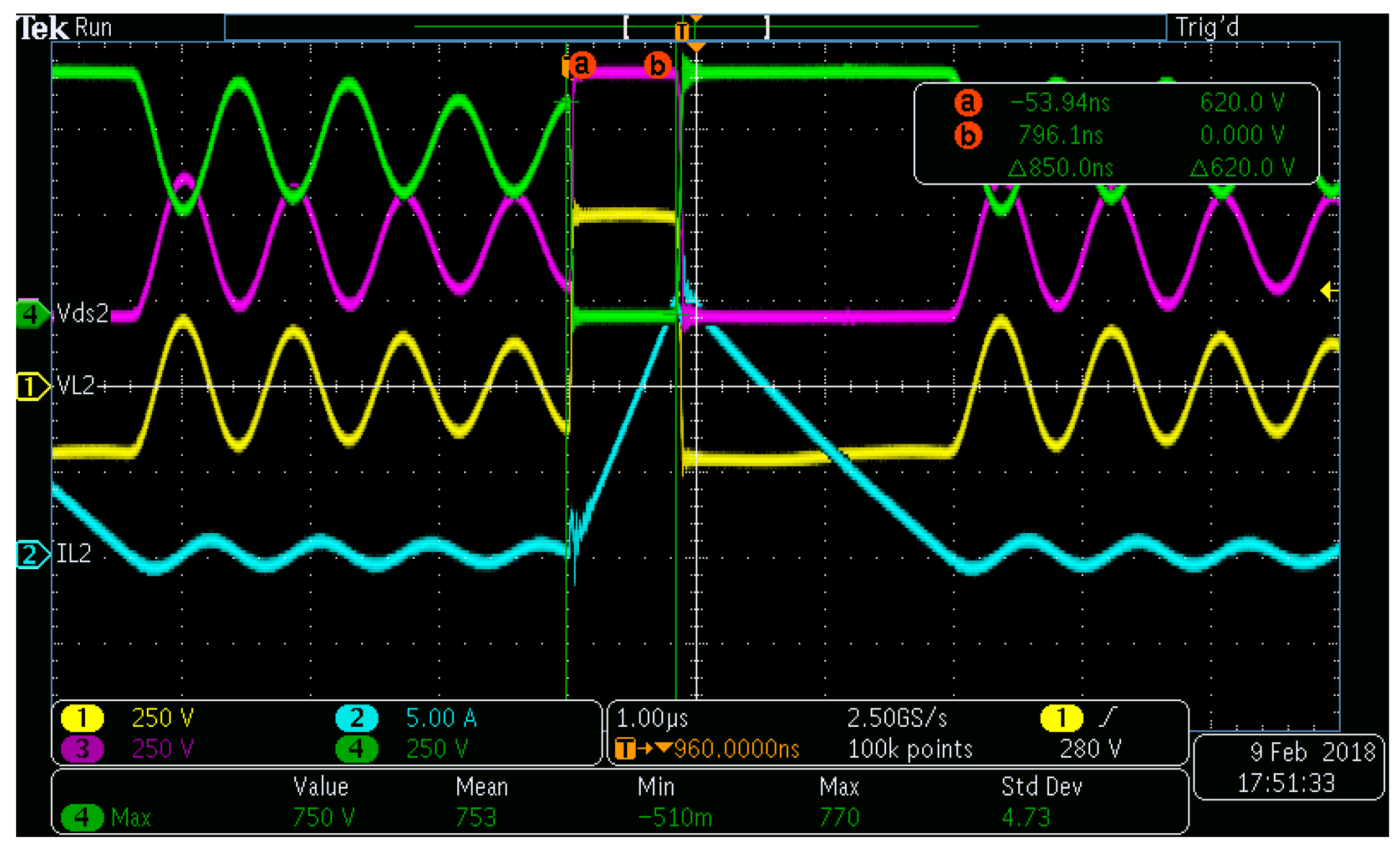
As it can be seen in these figures, the converter losses present some variations around 1.5 kW. Indeed, in the Discontinuous Conduction Mode, a voltage oscillation appears on the diode and both semiconductors are in the OFF state (Figure 12). Depending on the exact time of turning the MOSFET on again, the switching losses may be very different, due to the initial voltage.
Thanks to this measurement, a better model was built, in order to fit this behavior. Unfortunately, the oscillation depends on stray elements, which are not predictable in a predesign phase (devices capacitance, which are voltage dependent, inductor capacitance and circuit layout parasitic). Therefore, an averaging of this phenomenon was proposed, leading to a more robust model (Figure 13). Even if the exact behavior is not represented, the main variation is captured, which is the main goal of predesign. This example shows the importance of both experimental validation and iterative process in the method.
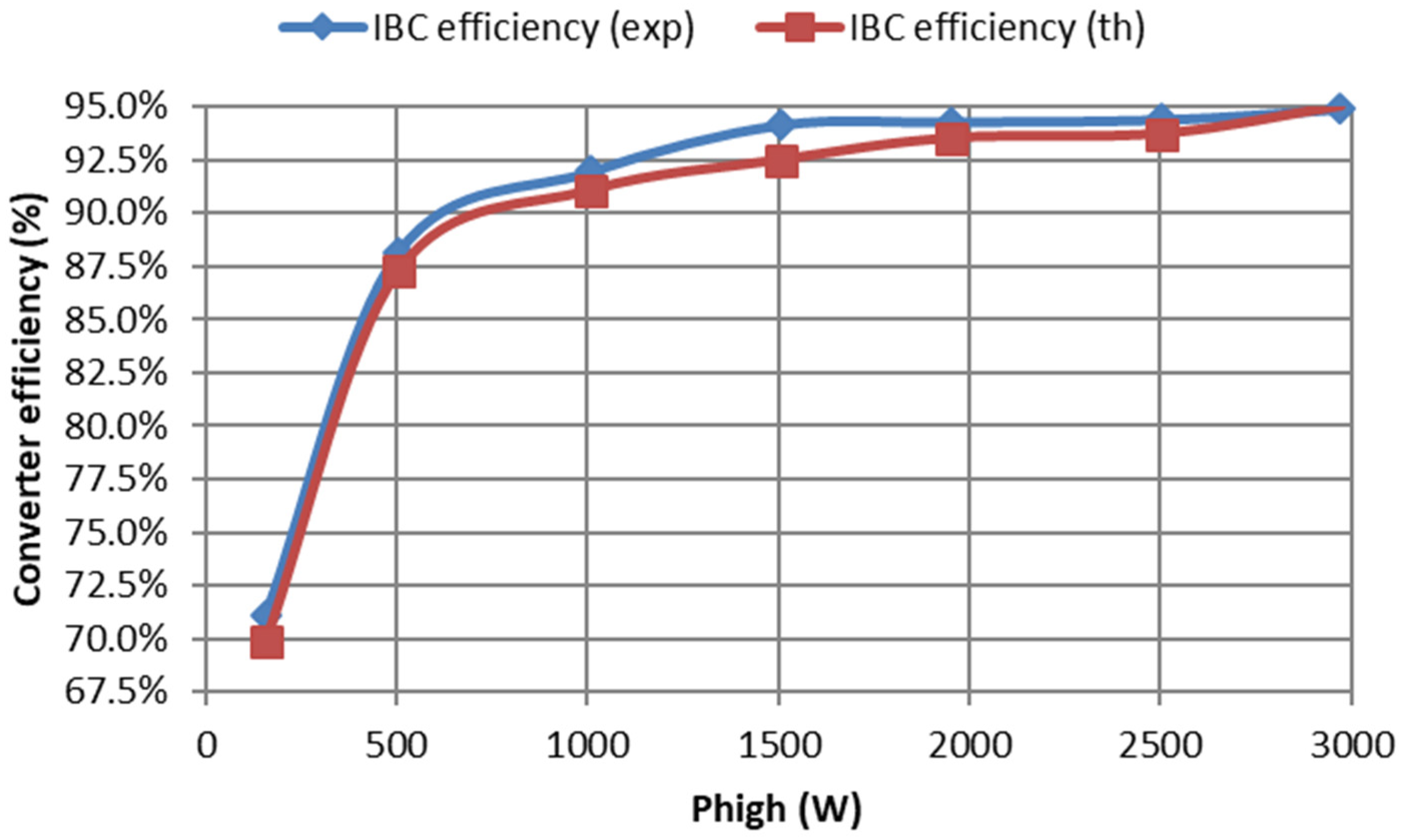
Figure 14 shows the converter global efficiency: the blue curve shows the experimental results and red curve the theoretical efficiency obtained with the optimization model. Both curves are very close: the converter model is considered as valid for the case study application.

6. Optimizations in the Imaginary World

Optimizations were performed with the initial set of specifications (Table 1 in Section 3.2.). These optimizations allow testing and understanding the optimization problem limits, and trying different technologies (in this section, we changed the magnetic material of the phase inductor).

6.1. Optimization Problem Set Up according to Initial Set of Specifications

Since the converter should operate on wide conditions (input and output voltage and current), there are not one but several sizing operating points (OP). In the discontinuous conduction mode and for the dedicated application, there are three of them. The first sizing operating point (OP #1) is when the converter is running at: full power (5 kW), maximum input voltage in the range [450–800] V (so at 800 V input voltage), minimum output voltage in the range [200–430] V (so at 200 V output voltage) and at maximum cold plate temperature in the range [−45–+65] °C (so at 65 °C cooling temperature). At this operating point OP #1, the converter efficiency and components temperature are the limiting constraints. The second sizing operating point (OP #2) is constraint by the maximum allowed THD at a third of maximum power, maximum input voltage and minimum output voltage. Finally, the constraint on the conduction mode (staying discontinuous for the whole operating range) at maximum power, minimum input voltage and maximum output voltage makes the third sizing operating point (OP #3).
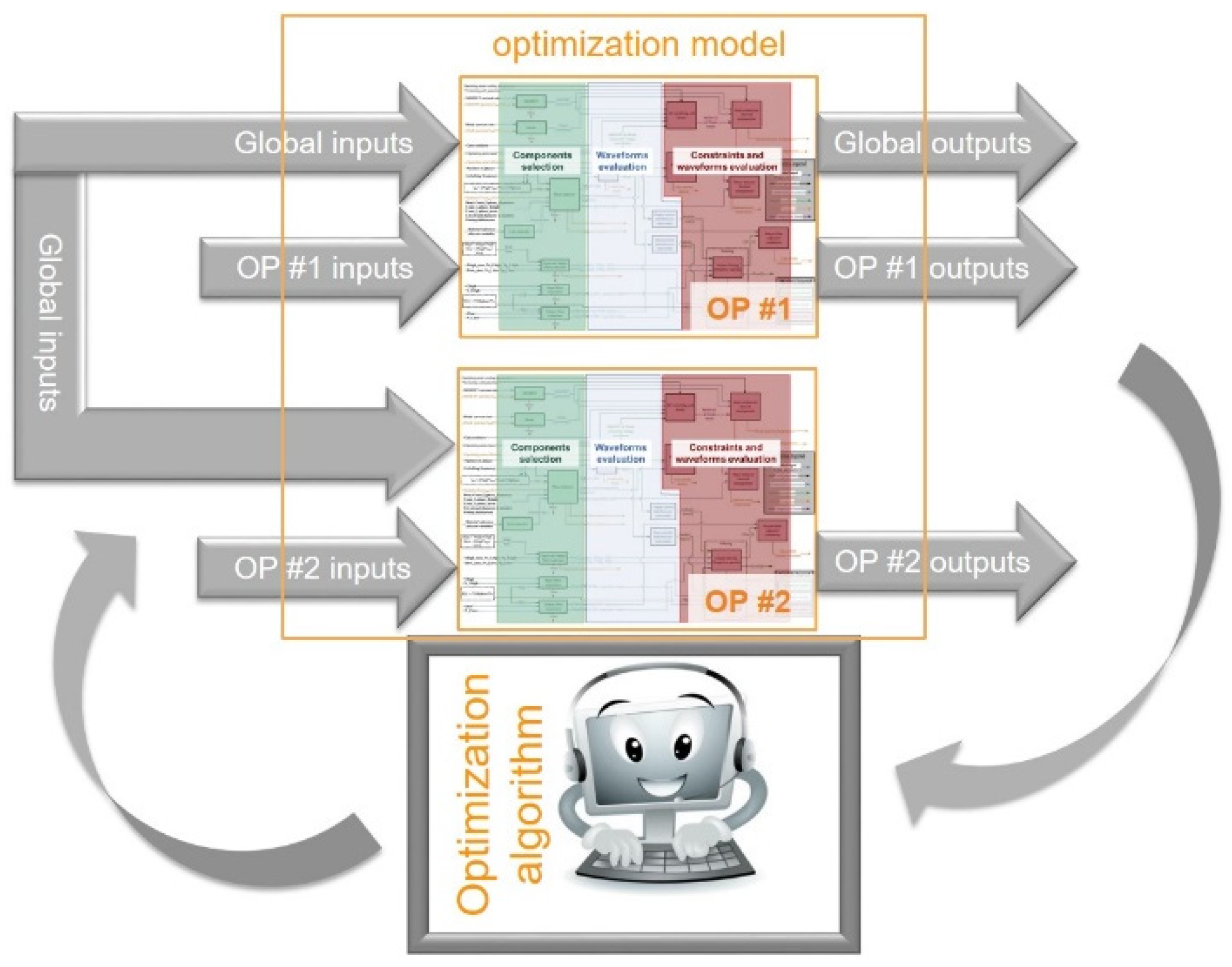
To optimize simultaneously the three sizing operating points, a new global model is created: the IBC model is called three times simultaneously with the same input design parameters and the global model output is made of the three set of constraints of each sizing OP in addition to the global mass of the converter to minimize. Figure 15 is an illustration of the global model in the case of two sizing operating points.
It should be noticed that the optimization problem can handle as much as sizing OP in the limit of the ability of the algorithm to handle NP optimization parameters (3), with NI the number of global input design variables, NC the number of constraints for one OP, NOP the number of sizing OP and NGO the number of global output.
N P = N I + N C N O P + N G O
In the case study, the optimization problem size with the three OP optimized simultaneously is: 36 input variables, 40 output constraints and 1 objective function.

6.2. Optimization in the Imaginary World Results

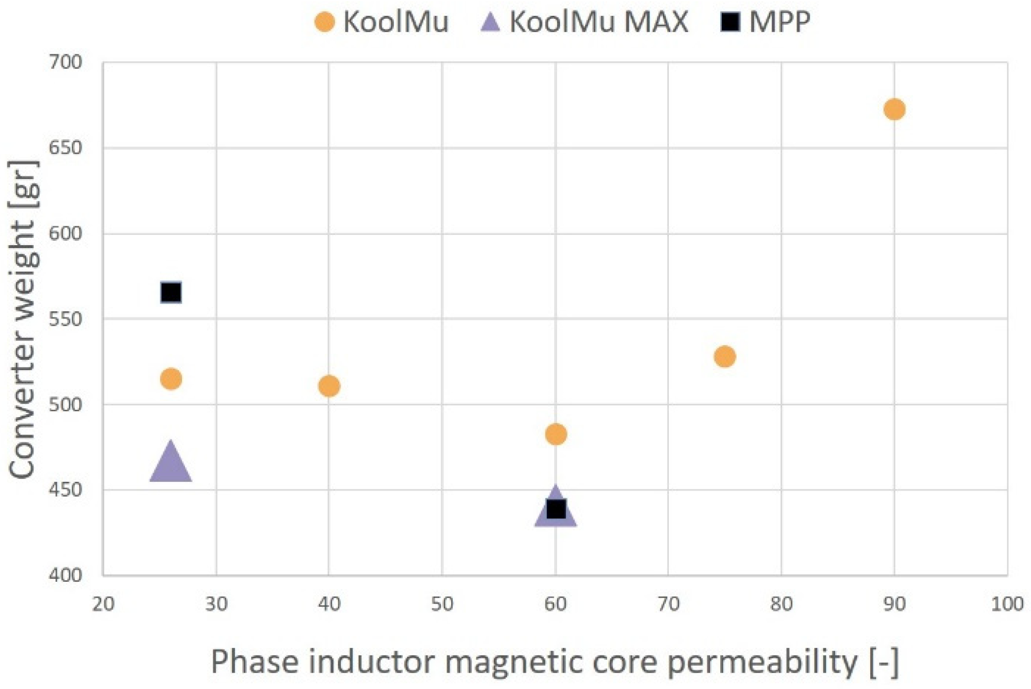
For the study case, eight different materials for the IBC phase inductor core were tested. Figure 16 summarizes the optimization results. Each one of the eight optimizations lasts less than 100 s with a classical PC and CADES 4.1.0 optimization framework [29].
The best optimization result is for the MPP 60 material (Kool Mu MAX 60 was close, but MPP a bit better) for the dedicated set of specifications, as summarized in Table 3. The weight repartition is: 70% for the phase inductors, 10% for the passive elements of the filter and 20% for the other parts (PCB, drivers, etc.).
Finally, the achieved weight density is 11.3 kW/kg in an imaginary world (with 3.2 phases). The optimizations are fast enough to negotiate the set of specifications in the imaginary world. Coming back to real world will use a discretization process detailed in Section 8.

7. Negotiation of the Set of Specifications

In this section, it is shown how the supplier’s designers can provide quantified curves to help the system integrator in the definition of the specifications. These curves show the evolution of converter performances according to the change in specification.

7.1. Specific Procedure for the Purpose

A script sweeps the specification variable and run optimization for each new point. The optimization result of the previous point (N − 1) is set as initial point for the SQP optimization point N. This technic helps to obtain a good convergence of the algorithm and obtain the results fast.

7.2. Examples of Specifications Negotiation in the Imaginary World

For each of the following results, the initial set of specifications is the basis and only one parameter is swept.

7.2.1. IBC Efficiency vs. Weight

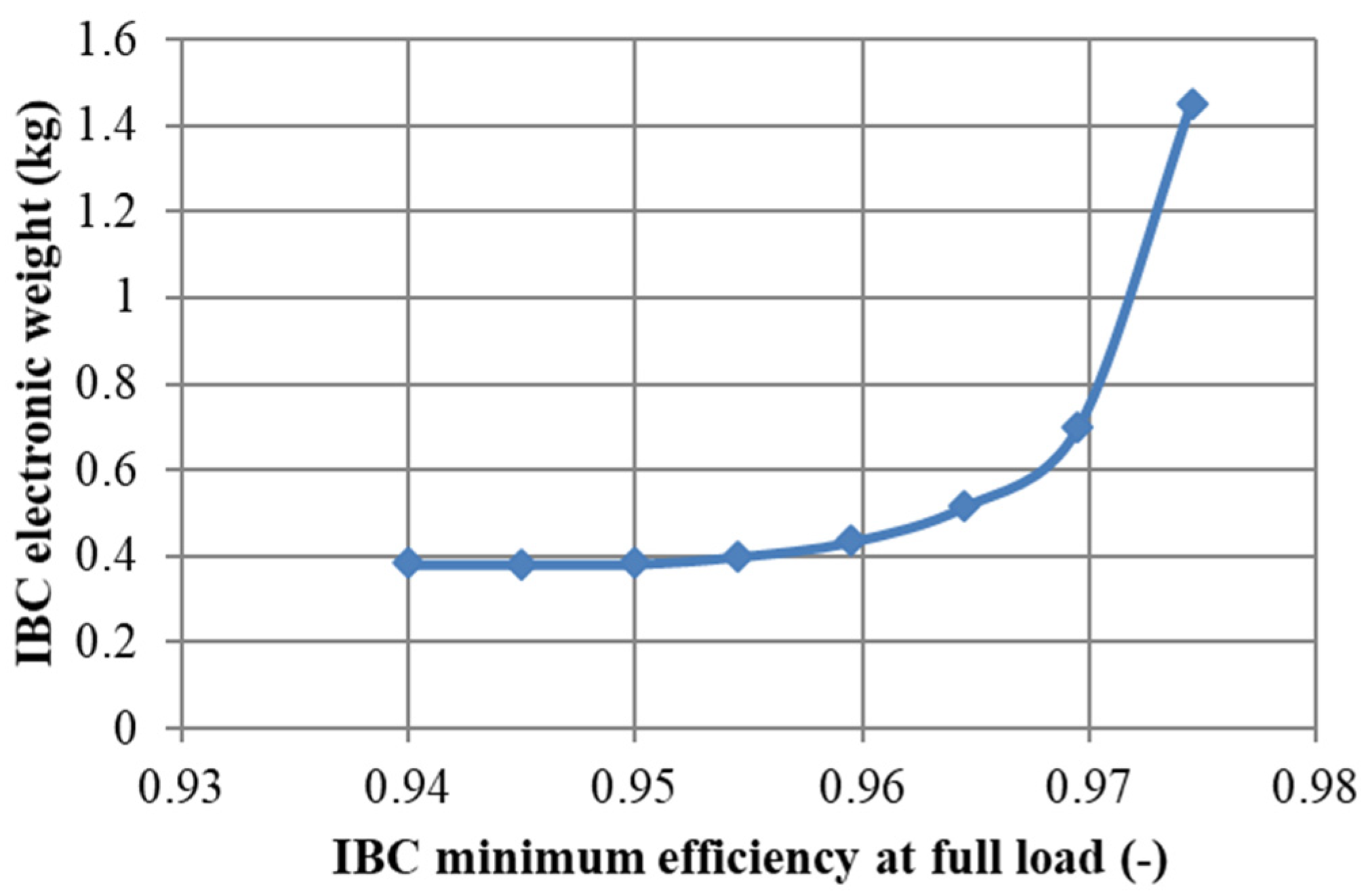
Generally, designers wish to maximize the efficiency and to minimize the weight of the converter for energy saving for embedded application. A curve showing the optimal points between these two antagonistic criteria is called a Pareto front (Figure 17). As expected, when the requirement on the IBC minimum efficiency at full power increases, the converter weight increases too.

7.2.2. Maximum Output Voltage vs. Weight

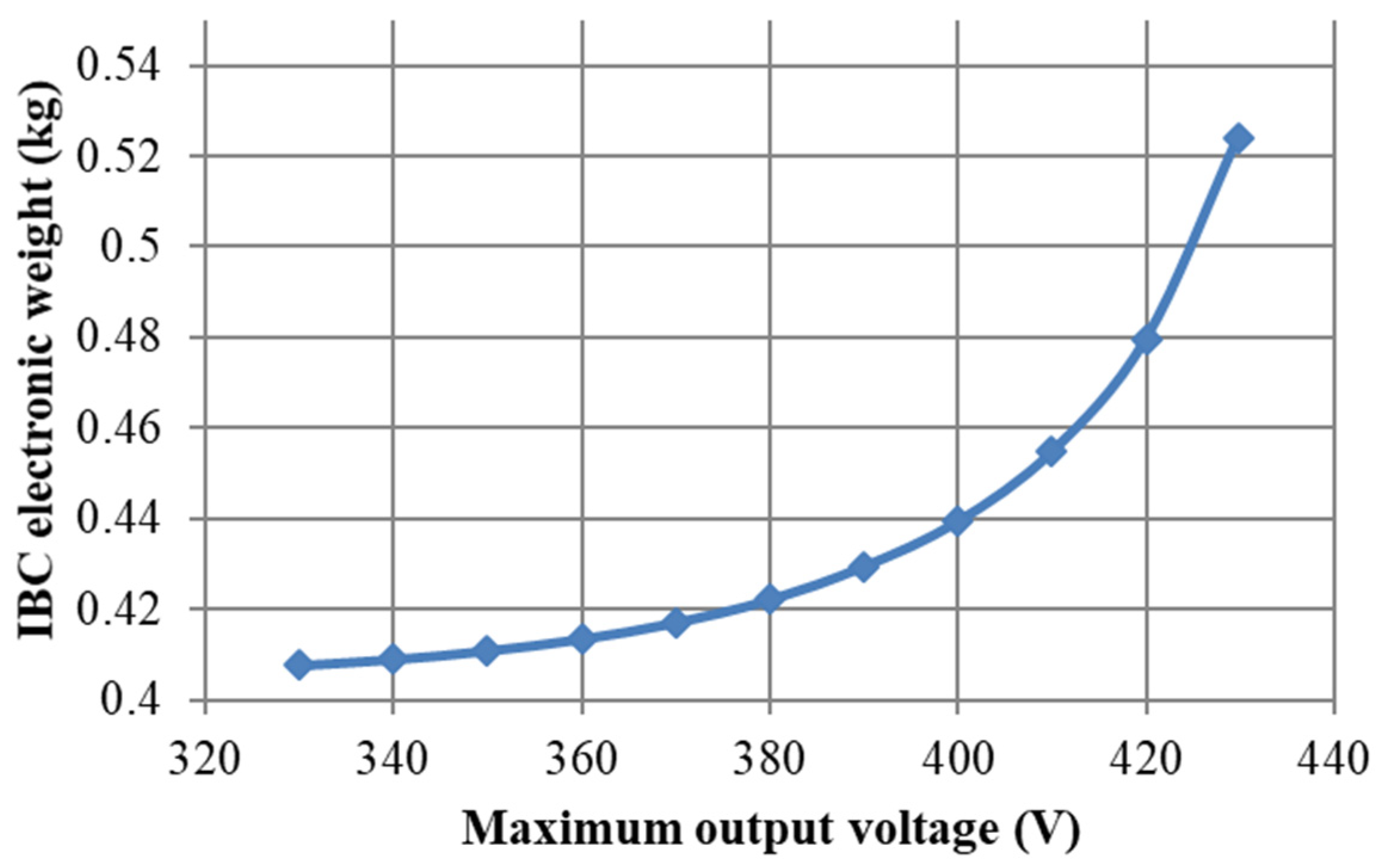
For the airship motors and stock units, it may be interesting to increase the output voltage range by increasing for example the maximum output voltage of the converter. Figure 18 shows the evolution of the weight of the converter according to this maximum output voltage. For all these optimizations, the input voltage range stays as in Table 1.
The converter weight increases, while the output voltage range increases. It is worth remembering that the converter must operate in discontinuous conduction mode for all operating conditions. When the maximum output voltage increase, the voltage distance between the input and output decreases. The optimization algorithm is forced to decrease the IBC switching frequency that conducts into the increase in passive elements.

7.2.3. Conclusions

In this paper, only two examples of the impact of specifications were provided, but a lot more can be imagined. Each curve was obtained in less than 2 min. The efficiency of the proposed approach helps to make the discussions more fluid during the preliminary design phase, between the power electronics engineer and the system provider.

8. Discretization Process

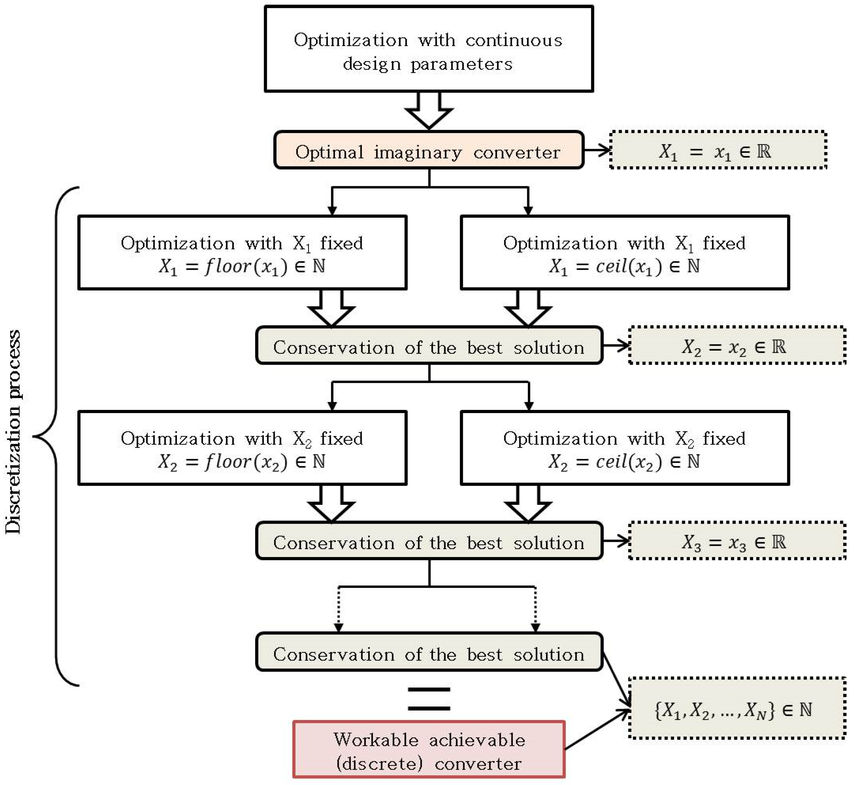
When the preliminary design phase is a success, designers must start the design phase. The proposed approach provides an optimization result in the imaginary world with only continuous design parameters. We propose here a discretization process to come back fast in the real world based on the optimal imaginary solution.
Figure 19 shows the proposed discretization process. It is actually the local research of a discrete solution (i.e., close to the imaginary one). The discretization starts with the most influent variable. Here, the number of phases, then the phase inductor core, the MOSFET, the diode, and finally filtering capacitors and inductors. Between each step of the discretization process, a new optimization is carried out to adjust the design variables to the discrete choice.
During this discretization process, the weight repartition is quite stable between the converter components. With the imaginary solution, the weight repartition was 69% for the phase inductors, 10% for filtering components and 21% for the other parts. With the real solution (i.e., last step of the process), the repartition is 72% for phase inductors, 10% for filtering and 18% for the other parts. It reveals that the proposed process respects the imaginary solution main characteristic (predictable since it is a local search method).

9. Conclusions

This paper showed how to use deterministic algorithms in the pre-design steps of power electronics converter. The ability of such algorithm to converge quickly to the optimal solution and to explore a wide space of solution is especially interesting in predesign phases, with such a large number of degrees of freedom. Since such algorithms necessitate gradients, continuous and derivable models were developed and validated with experimental setups. The problem formulation was explained and used in an actual example of constrained converter for a stratospheric use. The continuous and derivable models allow optimizing in an “imaginary world”, providing a kind of “theoretical optimum”, which is very interesting when discussing the initial specifications with the final user. Once requirements are negotiated, or when various technologies are compared and the final choice made, a discretization process is used to cope with the values available in the “real life”. It was shown in the considered example that the final design is not distant from the imaginary optimum.
The choice made in this paper of using SQP algorithms allows developing converter and components models with less constraints in terms of formulation than in Geometric Programing [8]. Therefore, they can be quite generic and used in other cases. For instance, the difference of models between the proposed application of IBC and a PWM inverter in [30] are not that much different. Even if the time necessary to develop such differentiable models is non negligible, the ability of exploring wide space of solutions, negotiating the constraints, handling several operating points simultaneously is a great advantage for the designer, which might be decisive for winning a proposal, or evaluating fairly several technologies for a given application. For the system designer, it also helps in evaluating the impact of system level constraints in the overall performances of the converter and the system.

Author Contributions

Conceptualization, F.W., J.-L.S. and M.D.; methodology, M.D., F.W., J.-L.S. and C.R.; software, M.D. and F.W., validation, M.D., C.R. and J.-L.S.; formal analysis, M.D. and T.D.; investigation, M.D., J.-L.S. and C.R.; resources, M.D.; data curation, M.D. and C.R.; writing—original draft preparation, M.D.; writing—review and editing, T.D. and J.-L.S.; visualization, M.D., supervision, J.-L.S. and F.W.; project administration, J.-L.S.; funding acquisition, J.-L.S. All authors have read and agreed to the published version of the manuscript.

Funding

The authors would like to thank Tronico-Alcen for their funding and case study support.

Institutional Review Board Statement

Not applicable.

Informed Consent Statement

Not applicable.

Data Availability Statement

Not applicable.

Conflicts of Interest

The authors declare no conflict of interest.

References

  1. Kolar, J.W.; Biela, J.; Waffler, S.; Friedli, T.; Badstuebner, U. Performance trends and limitations of power electronic systems. In Proceedings of the 2010 6th International Conference on Integrated Power Electronics Systems, Nuremberg, Germany, 16–18 March 2010; pp. 1–20. [Google Scholar]
  2. Berliner, C.; Brimson, J.A. Cost Management for Today’s Advanced Manufacturing: The CAM-I Conceptual Design; Harvard Business School Press: Boston, MA, USA, 1988. [Google Scholar]
  3. Kline, W.A.; Schindel, W.D. Engineering design, a shift from a process to a model-based view. In Proceedings of the 2017 IEEE Frontiers in Education Conference (FIE), Indianapolis, IN, USA, 18–21 October 2017; pp. 1–3. [Google Scholar]
  4. Delhommais, M. Review of optimization methods for the design of power electronics systems. In Proceedings of the European Conference on Power Electronics and Application, Lyon, France, 7–11 September 2020. [Google Scholar]
  5. Marchand, C.; Coquery, G.; Larouci, C.; Bendali, M.; Azib, T. Design methodology of an interleaved buck converter for onboard automotive application, multi-objective optimisation under multi-physic constraints. IET Electr. Syst. Transp. 2015, 5, 53–60. [Google Scholar]
  6. Li, X.; Zhang, X.; Lin, F.; Blaabjerg, F. Artificial-Intelligence-Based Design for Circuit Parameters of Power Converters. IEEE Trans. Ind. Electron. 2021, 69, 11144–11155. [Google Scholar] [CrossRef]
  7. Busquets-Monge, S.; Crebier, J.-C.; Ragon, S.; Hertz, E.; Boroyevich, D.; Gurdal, Z.; Arpilliere, M.; Lindner, D. Design of a Boost Power Factor Correction Converter Using Optimization Techniques. IEEE Trans. Power Electron. 2004, 19, 1388–1396. [Google Scholar] [CrossRef]
  8. Stupar, A.; McRae, T.; Vukadinovic, N.; Prodic, A.; Taylor, J.A. Multi-Objective Optimization of Multi-Level DC–DC Converters Using Geometric Programming. IEEE Trans. Power Electron. 2019, 34, 11912–11939. [Google Scholar] [CrossRef]
  9. Baurreau, F.; Staraj, R.; Ferrero, F.; Lizzi, L.; Ribero, J.M.; Chessel, J.P. Stratospheric platform for telecommunication missions. In Proceedings of the IEEE Antennas and Propagation Society AP-S International Symposium, Vancouver, BC, Canada, 19–24 July 2015; pp. 914–915. [Google Scholar]
  10. Thales, “Space Q & A: All about Stratobus”. 2017. Available online: https://www.thalesgroup.com/en/worldwide/space/news/space-qa-all-about-stratobus (accessed on 13 June 2017).
  11. Mühlethaler, J.; Biela, J.; Kolar, J.W.; Ecklebe, A. Improved core loss calculation for magnetic components employed in power electronic system. In Proceedings of the Twenty-Sixth Annual IEEE Applied Power Electronics Conference and Exposition (APEC), Fort Worth, TX, USA, 6–11 March 2011; pp. 1729–1736. [Google Scholar]
  12. Voldoire, A.; Schanen, J.L.; Ferrieux, J.P.; Sarrazin, B.; Gautier, C. Predesign Methodology of Voltage Inverters using a Gradient-Based Optimization Algorithm. IEEE J. Emerg. Sel. Top. Power Electron. 2021, 9, 5895–5905. [Google Scholar] [CrossRef]
  13. Delhommais, M.; Schanen, J.-L.; Wurtz, F.; Rigaud, C.; Chardon, S. Design by Optimization Methodology: Application to a Wide Input and Output Voltage Ranges Interleaved Buck Converter. In Proceedings of the Energy Conversion Congress & Exposition, Cincinnati, OH, USA, 1–5 October 2017; pp. 1–8. [Google Scholar]
  14. Enciu, P.; Gerbaud, L.; Wurtz, F. Automatic differentiation for sensitivity calculation in electromagnetism: Application for optimization of a linear actuator. IEEE Trans. Magn. 2011, 47, 1238–1241. [Google Scholar] [CrossRef]
  15. Gerbaud, L.; Baraston, A.; Schanen, J.; Delhommais, M. Selectivity in Frequency Modelling of Electrical Circuit for the Sizing by Optimization of Emc Filter for Power Electronics. In Proceedings of the Electrimacs, Toulouse, France, 4–6 July 2017; pp. 2–7. [Google Scholar]
  16. Boggs, P.T.; Tolle, J.W. Sequential Quadratic Programming. Acta Numer. 1996, 4, 1–52. [Google Scholar] [CrossRef] [Green Version]
  17. Zhang, S.; Yu, X. The Output Current Analysis and Its Applications in the Interleaved Boost Converter; Institute of Electrical and Electronics Engineers: Scottsdale, AZ, USA, 2012; pp. 1–5. [Google Scholar] [CrossRef]
  18. Choe, G.-Y.; Kim, J.-S.; Kang, H.-S.; Lee, B.-K. An Optimal Design Methodology of an Interleaved Boost Converter for Fuel Cell Applications. J. Electr. Eng. Technol. 2010, 5, 319–328. [Google Scholar] [CrossRef] [Green Version]
  19. Zhang, S.; Yu, X. A Unified Analytical Modeling of the Interleaved Pulse Width Modulation (PWM) DC-DC Converter and Its Applications. IEEE Trans. Power Electron. 2013, 28, 5147–5158. [Google Scholar] [CrossRef]
  20. Venkatachalam, K.; Sullivan, C.R.; Abdallah, T.; Tacca, H. Accurate prediction of ferrite core loss with non sinusoidal waveforms using only steinmetz parameters. In Proceedings of the IEEE Workshop on Computers in Power Electronics, COMPEL, Portland, OR, USA, 14 August 2002; pp. 36–41. [Google Scholar]
  21. New England Wire Technologies, “Litz Wire Theory”. 2017. Available online: https://www.newenglandwire.com/products/litz-wire-and-formed-cables/theory (accessed on 13 June 2017).
  22. Voldoire, A.; Schanen, J.; Ferrieux, J.-P.; Rizet, C.; Gautier, C.; Saber, C. Validation of Inductor Analytical Loss Models under Saturation Conditions for PWM Inverter. In Proceedings of the 21th European Power Electronics and Applications, in Acceptance Process, Genova, Italy, 3–5 September 2019; Volume 2, pp. 2–7. [Google Scholar]
  23. Delhommais, M.; Schanen, J.-L.; Wurtz, F.; Rigaud, C.; Chardon, S.; Vighetti, S. Thermal model of Litz wire toroidal inductor based on experimental measurements. In Proceedings of the IEEE Applied Power Electronics Conference and Exposition (APEC), San Antonio, TX, USA, 4–8 March 2018. [Google Scholar]
  24. Kyaw, P.A.; Delhommais, M.; Qiu, J.; Sullivan, C.R.; Schanen, J.; Rigaud, C. Thermal Modeling of Inductor and Transformer Windings Including Litz Wire. J. Submitt. IEEE Trans. Power Electron. 2019, 35, 1–38. [Google Scholar] [CrossRef]
  25. Delhommais, M.; Schanen, J.; Wurtz, F.; Rigaud, C.; Chardon, S. First Order Design by Optimization Method: Application to an Interleaved Buck Converter and Validation. In Proceedings of the IEEE Applied Power Electronics Conference and Exposition (APEC), San Antonio, TX, USA, 4–8 March 2018; pp. 944–951. [Google Scholar]
  26. Peng, K.; Santi, E. Performance Projection and Scalable Loss Model of SiC MOSFETs and SiC Schottky Diodes. In Proceedings of the IEEE Electric Ship Technologies Symposium, Old Town Alexandria, VA, USA, 21–24 June 2015; pp. 281–286. [Google Scholar]
  27. Peng, K.; Eskandari, S.; Santi, E. Analytical loss model for power converters with SiC MOSFET and SiC schottky diode pair. In Proceedings of the 2015 IEEE Energy Conversion Congress and Exposition (ECCE), Montreal, QC, Canada, 20–24 September 2015; pp. 6153–6160. [Google Scholar]
  28. Coutel, C.; Wurtz, F.; Bigeon, J. A comparative study of two methods for constrained optimisation with analytical models dealing with implicit parameters. IEEE Trans. Magn. 1999, 35, 1738–1741. [Google Scholar] [CrossRef]
  29. Vesta System, “CADES 4” . 2019. Available online: http://www.cades-solutions.com/?page_id=390 (accessed on 1 September 2019).
  30. Voldoire, A.; Schanen, J.-L.; Ferrieux, J.-P.; Derbey, A.; Gautier, C. Three-Phase PWM Voltage-Source-Inverter Weight Optimization for Aircraft Application Using Deterministic Algorithm. Electronics 2020, 9, 1393. [Google Scholar] [CrossRef]
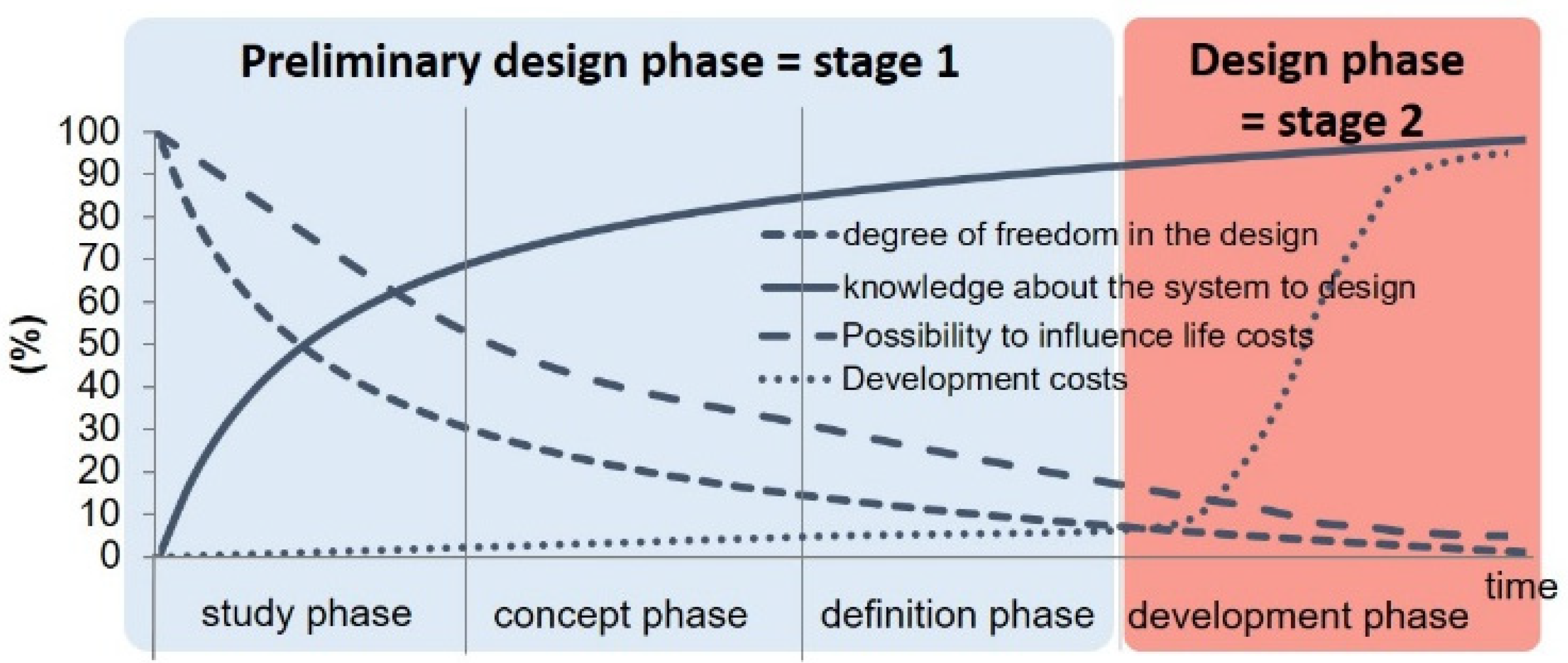
Figure 1. Design process paradox and timeline expenditure.
Designs 06 00068 g001
Figure 2. Discrete Pareto front of a DC-DC Interleaved Buck Converter obtained with a stochastic NSGA-II algorithm. Reprinted and adapted with permission from Larouci, C., 2022, Ref. [5].
Designs 06 00068 g002
Figure 3. Description of the proposed approach.
Designs 06 00068 g003
Figure 4. Stratobus electrical architecture illustration made from technical description in [10].
Designs 06 00068 g004
Figure 5. Interleaved Buck Converter schematic.
Designs 06 00068 g005
Figure 6. Power electronics sub-system models preferred organization for the proposed approach.
Designs 06 00068 g006
Figure 7. Formulation of the input filtering capacitors selection model.
Designs 06 00068 g007
Figure 8. Example of datasheet interpolation.
Designs 06 00068 g008
Figure 9. Two-dimensional thermal model of the toroidal phase inductor.
Designs 06 00068 g009
Figure 10. Variation of MOSFET ON state resistance according to its current rating (left) and (right) junction temperature.
Designs 06 00068 g010
Figure 11. Repartition of the losses inside the phase #2 of the 3-Phase IBC prototype: the semiconductors losses are thermally measured and phase inductor losses electrically measured.
Designs 06 00068 g011
Figure 12. Oscilloscope screenshot. Prototype working at 700–200 V 2187 W. Yellow trace is the phase inductor #2 voltage, the blue trace its current, the purple trace the diode reverse voltage and the green trace the MOSFET drain-source voltage.
Designs 06 00068 g012
Figure 13. Repartition of the losses inside a phase of the 3-Phase IBC prototype according to optimization model.
Designs 06 00068 g013
Figure 14. Prototype global efficiency at input voltage 700 V and output voltage 200 V; input power swept from 160 W to 2970 W.
Designs 06 00068 g014
Figure 15. Example of global optimization model of a converter to handle 2 sizing operating points simultaneously.
Designs 06 00068 g015
Figure 16. Optimizations in the imaginary world results for 8 different inductor core materials.
Designs 06 00068 g016
Figure 17. Pareto front between the weight and the efficiency of the IBC in DCM mode with MPP 60 material for phase inductor core based on the initial set of specifications of Table 1.
Designs 06 00068 g017
Figure 18. Parameterized optimization in the imaginary world of the IBC weight VS its maximum output voltage requirement.
Designs 06 00068 g018
Figure 19. Proposed discretization process to come back in the real world.
Designs 06 00068 g019
Table 2. IBC input design variables.
Design ParameterAbbreviationNb of Discrete Choices
Switching frequencyFs-
Number of IBC PhaseNBphaseN6
Conduction modeCDT2
Inductor core materialMaterialT3
Inductor core main permeabilities (14, 26, 40, 60, 125)MaterialD5
Toroidal inductor core size (External/Internal diameter/Height)DoutD, DinD, HD~36
Litz strand diameter (AWG 33, 36, 38, 40, 42)DlitzLphaseD5
Litz number of strandsnstrandLphaseN15
Phase inductor number of turnsNturnsLphaseN~100
SiC 1200 V MOSFET current ratingCal_ImosD5
SiC 1200 V Schottky diode current ratingCal_IdiodeD10
Input single capacitor valueChighD17
Output single capacitor valueClowD46
Number of input capacitors in parallelN_ChighN15
Number of output capacitors in parallelN_ClowN15
Input single filtering inductor value @ 0ALhigh_maxD17
Output single filtering inductor value @ 0ALlow_maxD17
Number of input inductors in seriesNs_LhighN5
Number of output inductors in seriesNs_LlowN5
Number of input inductors in parallelNp_LhighN5
Table 3. IBC optimal imaginary solutions for the initial set of specifications.
MaterialMPP 60
Optimization iterations (#)10
Optimization time (s)75
Converter weight (gr)439
Switching frequency (kHz)164
number of phases3.2
Inductor value (µH)33.6
Publisher’s Note: MDPI stays neutral with regard to jurisdictional claims in published maps and institutional affiliations.