Permittivity of 3D-Printed Nylon Substrates with Different Infill Patterns and Densities for Design of Microwave Components


Abstract
1. Introduction
1.1. How Does Infill Density Impact the Permittivity of an AM Substrate?
1.2. How Does Infill Pattern Impact the Permittivity of an AM Substrate?
1.3. How Does Roof and Floor Layer Impact the Permittivity of a Solid Infill Pattern AM Substrate?
2. Materials and Methods
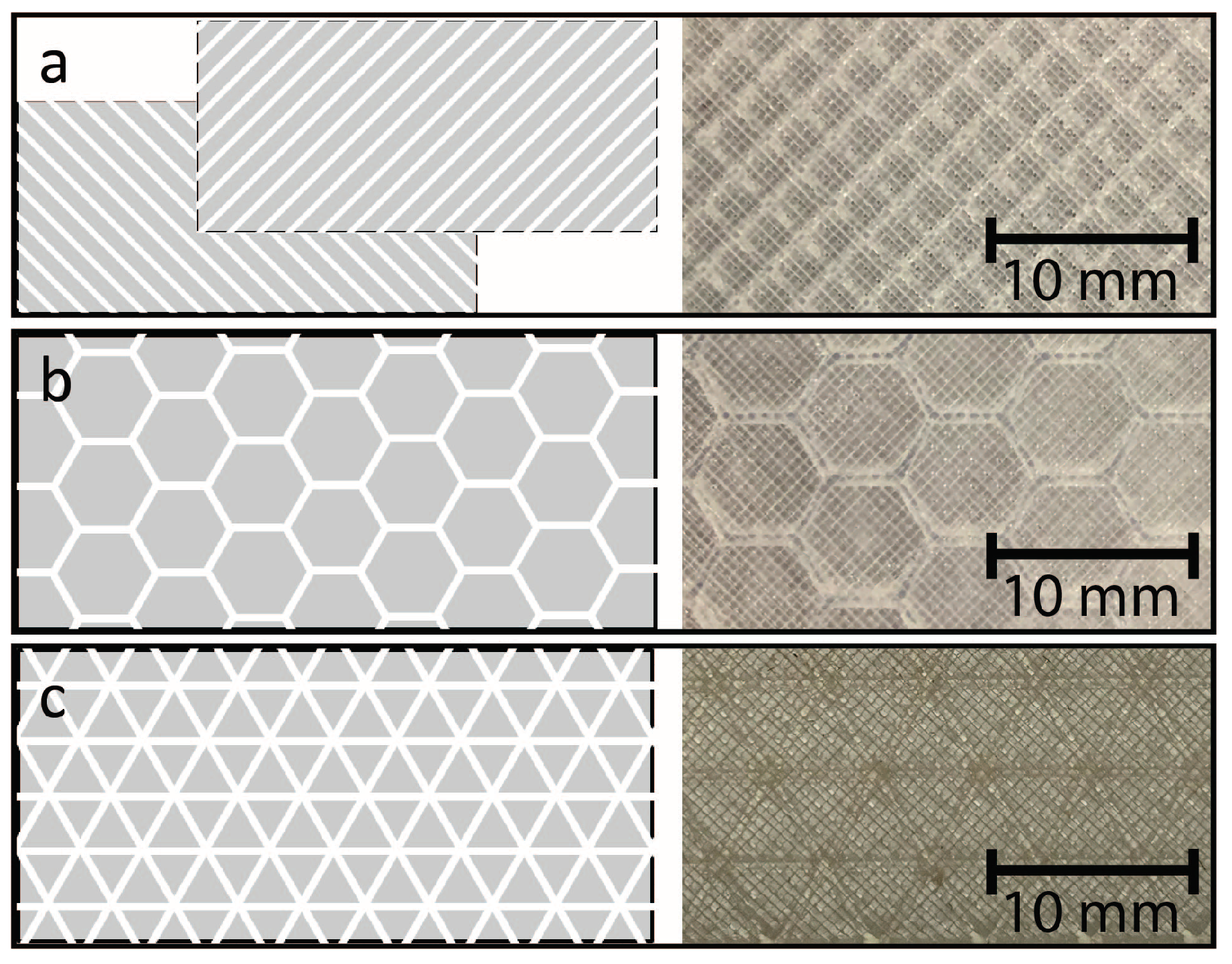
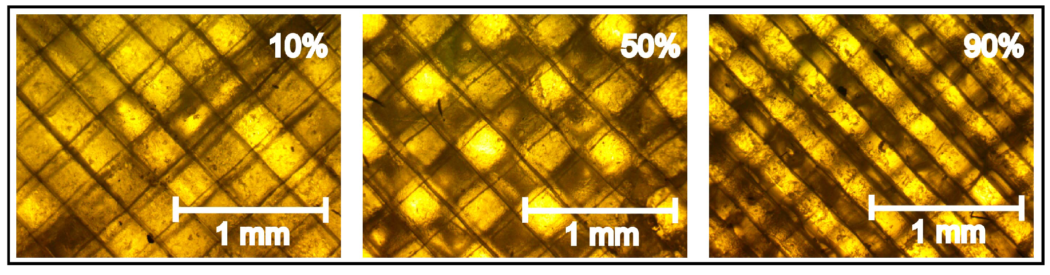
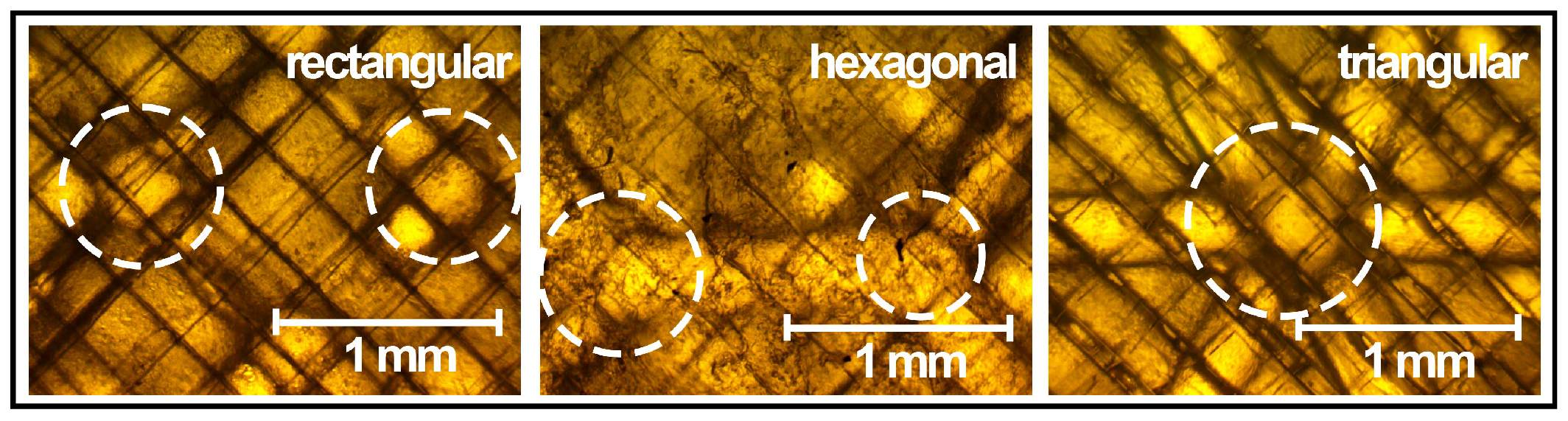
2.1. Specimen Design and Preparation
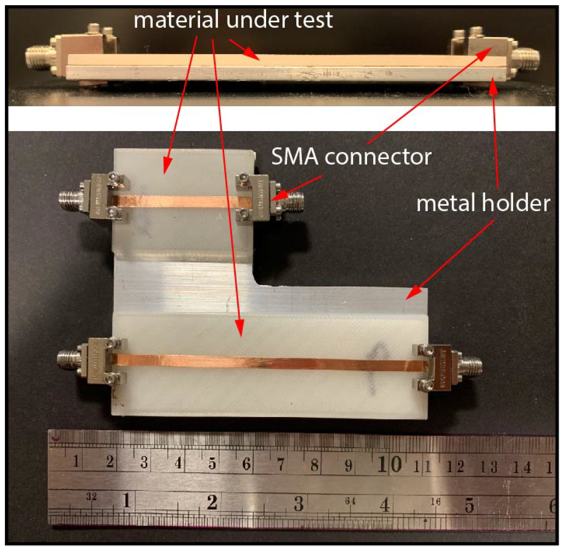
2.2. Permittivity Measurement of AM Material
3. Results and Discussion
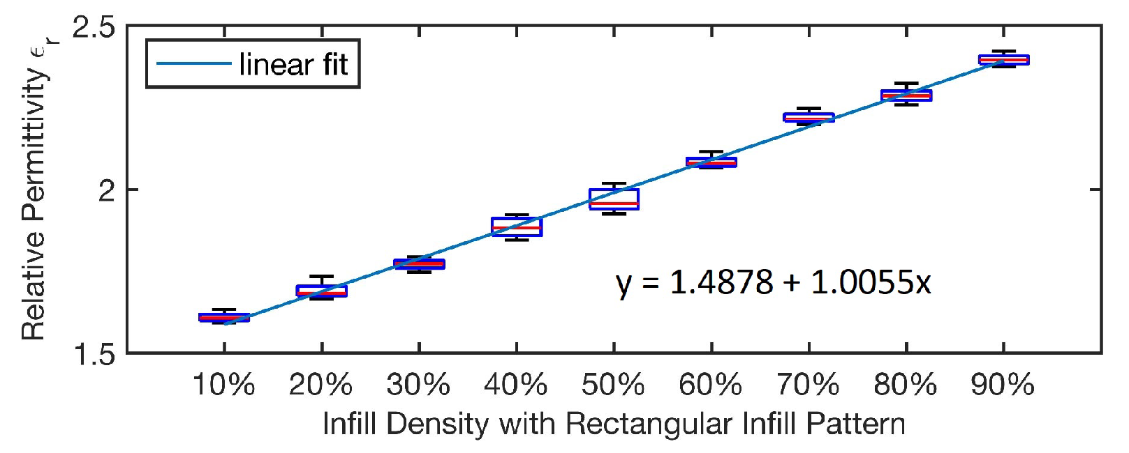
3.1. Research Question 1
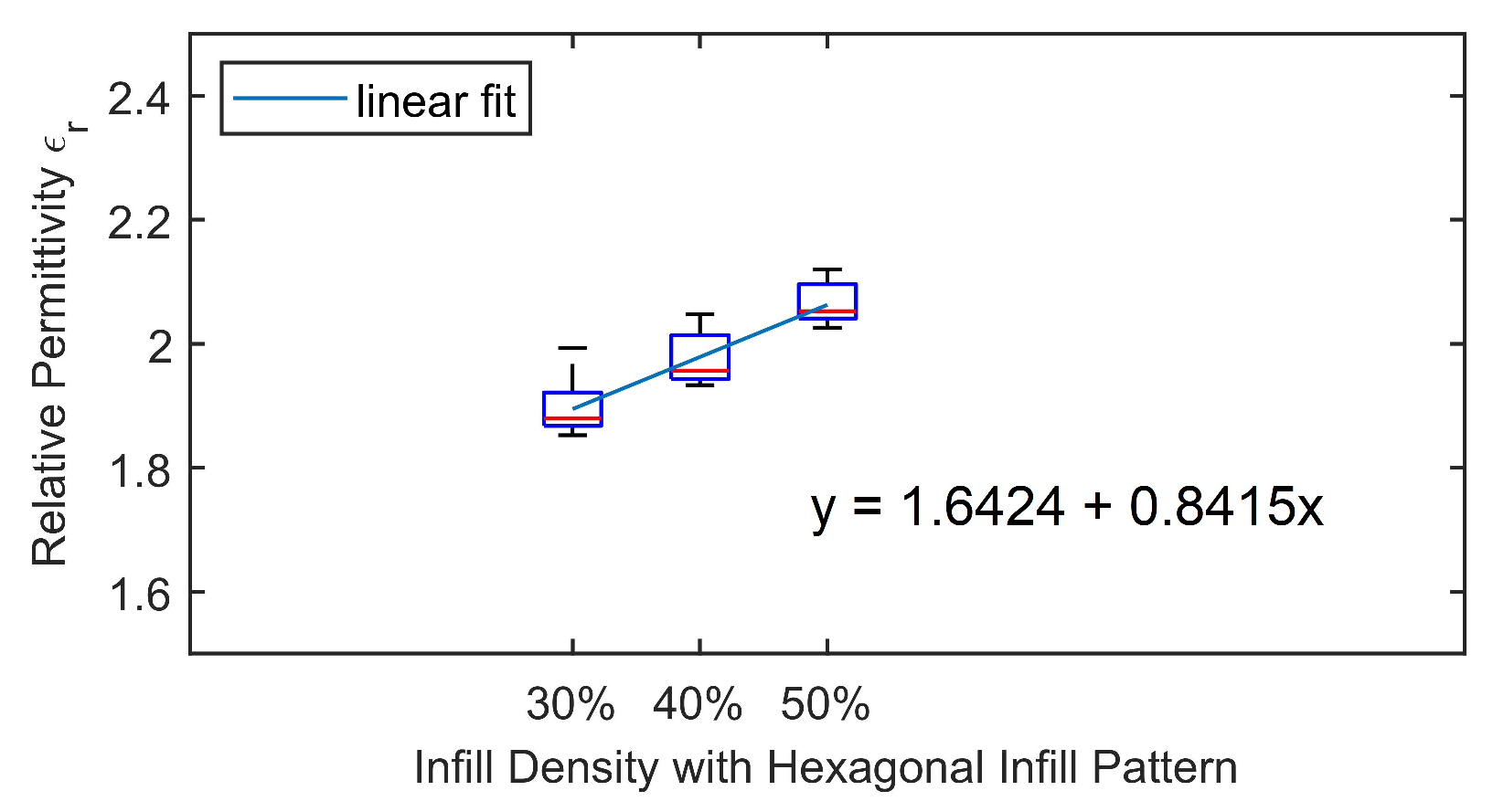
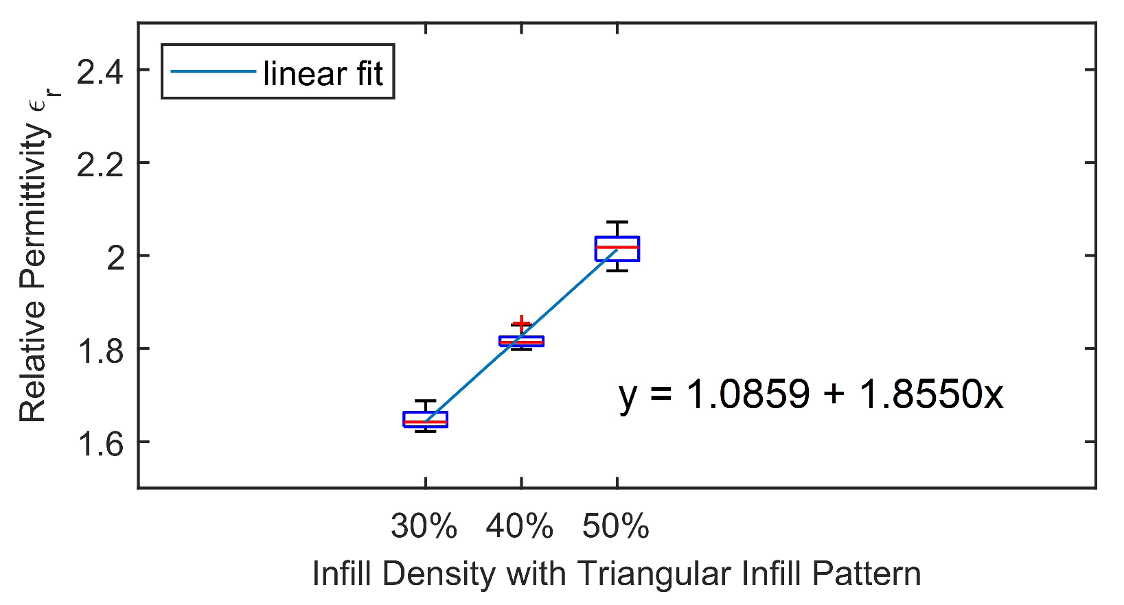
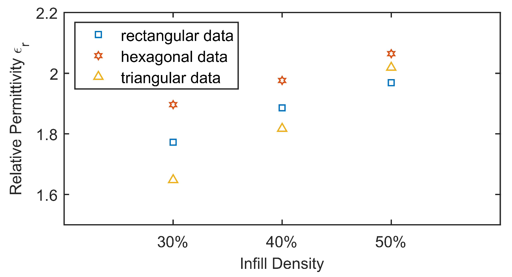
3.2. Research Question 2
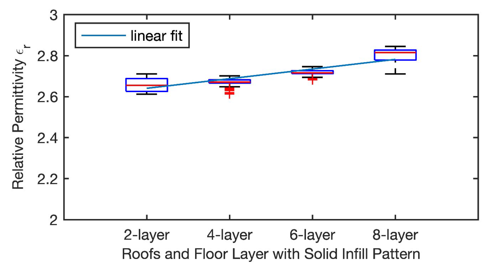
3.3. Research Question 3
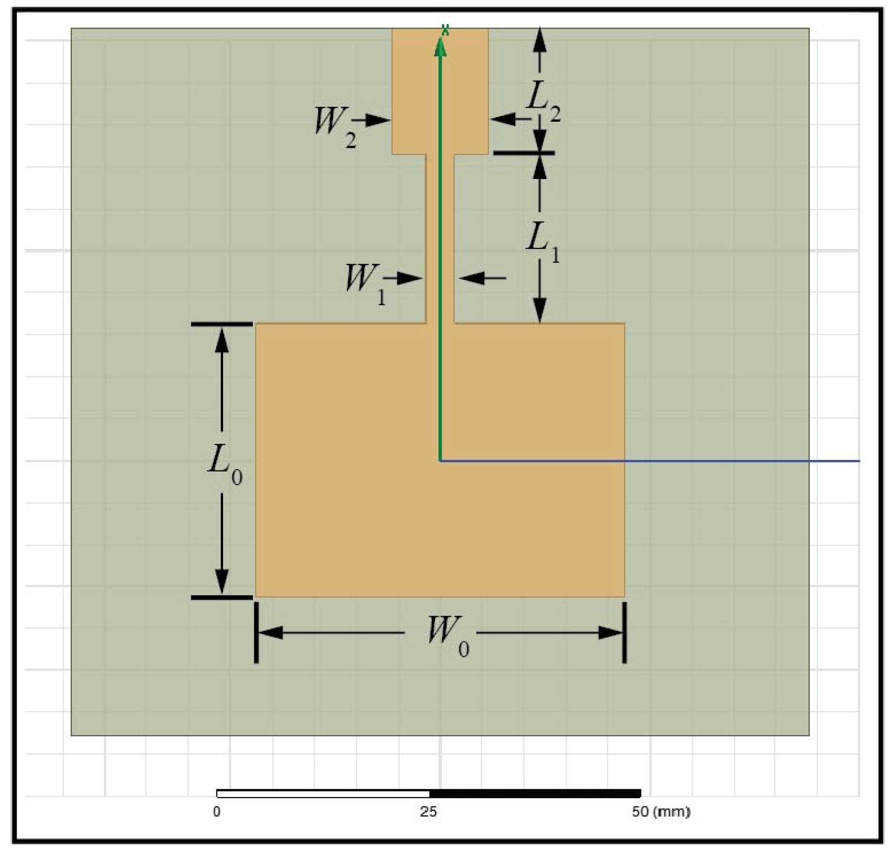
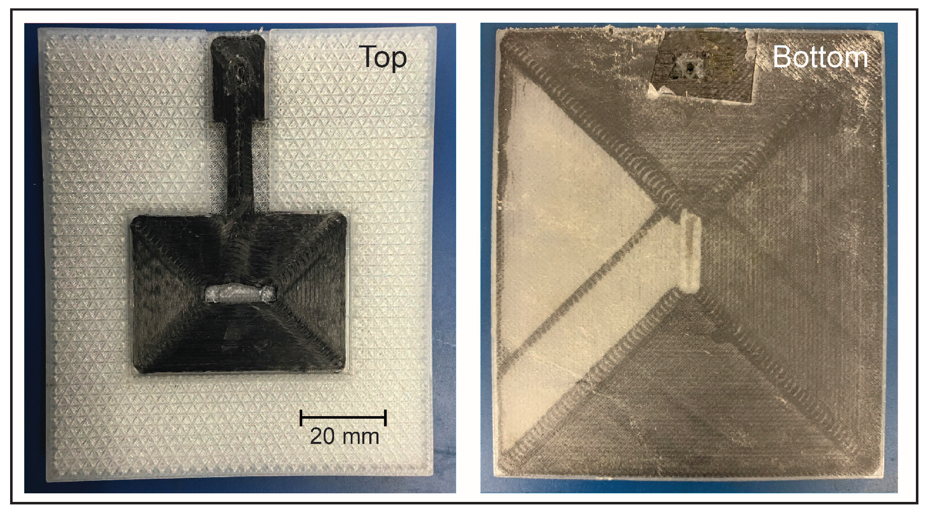
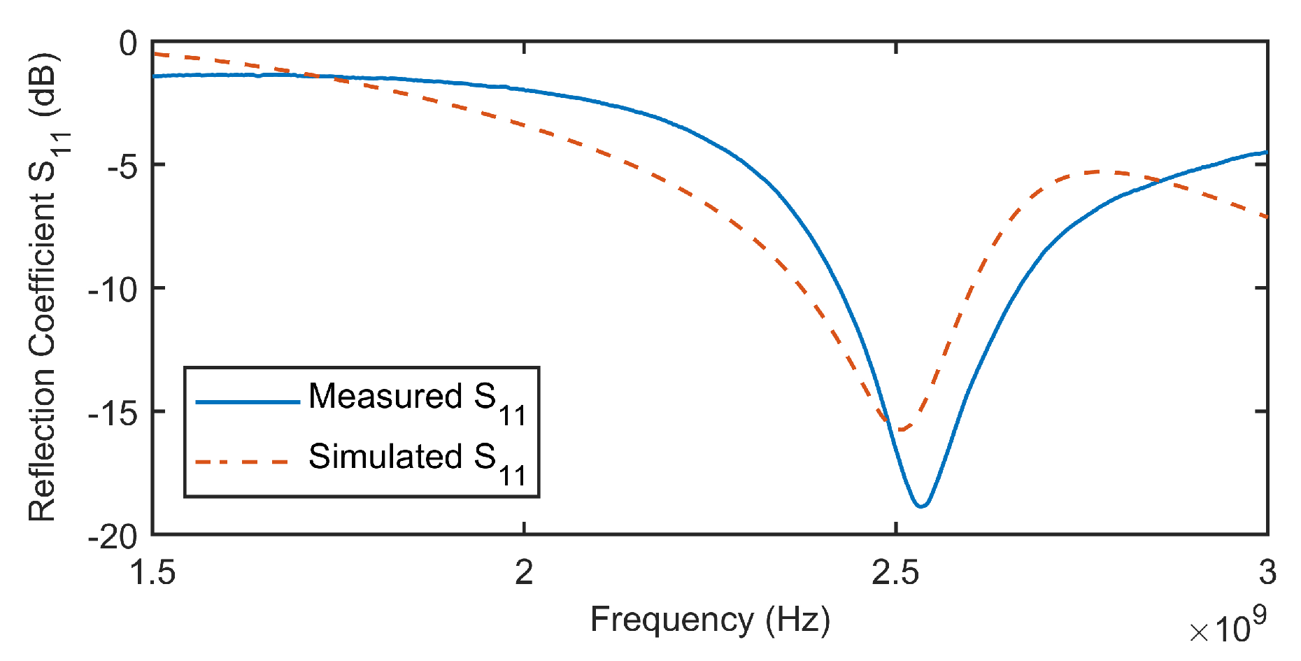
4. Case Study: AM Patch Antenna Design
5. Conclusions
Author Contributions
Funding
Acknowledgments
Conflicts of Interest
References
- Atzeni, E.; Salmi, A. Economics of additive manufacturing for end-usable metal parts. Int. J. Adv. Manuf. Technol. 2012, 62, 1147–1155. [Google Scholar] [CrossRef]
- Klahn, C.; Leutenecker, B.; Meboldt, M. Design strategies for the process of additive manufacturing. Procedia CIRP 2015, 36, 230–235. [Google Scholar] [CrossRef]
- Macdonald, E.; Salas, R.; Espalin, D.; Perez, M.; Aguilera, E.; Muse, D.; Wicker, R.B. 3D printing for the rapid prototyping of structural electronics. IEEE Access 2014, 2, 234–242. [Google Scholar] [CrossRef]
- Yu, Y.Z.; Lu, J.R.; Liu, J. 3D printing for functional electronics by injection and package of liquid metals into channels of mechanical structures. Mater. Des. 2017, 122, 80–89. [Google Scholar] [CrossRef]
- Conner, B.P.; Manogharan, G.P.; Martof, A.N.; Rodomsky, L.M.; Rodomsky, C.M.; Jordan, D.C.; Limperos, J.W. Making sense of 3-D printing: Creating a map of additive manufacturing products and services. Addit. Manuf. 2014, 1, 64–76. [Google Scholar] [CrossRef]
- Manessis, D.; Podlasly, A.; Ostmann, A.; Aschenbrenner, R.; Lang, K.D. Large-scale manufacturing of embedded subsystems-in-substrates and a 3D-stacking approach for a miniaturised medical system integration. In Proceedings of the 2013 Eurpoean Microelectronics Packaging Conference (EMPC), Grenoble, France, 9–12 September 2013; pp. 1–6. [Google Scholar]
- O’Brien, J.M.; Rojas, E.; Weller, T.M. A switched-line phase shifter fabricated with additive manufacturing. In Proceedings of the International Symposium on Microelectronics 2013, Orlando, FL, USA, 30 September–3 October 2013; International Microelectronics Assembly and Packaging Society: Research Triangle Park, NC, USA, 2013; Volume 2013, pp. 909–913. [Google Scholar]
- Robles Dominguez, U. 3D Printed Impedance Elements by Micro-Dispensing. Ph.D. Thesis, Electrical Engineering, University of Texas at El Paso, El Paso, TX, USA, 2013. [Google Scholar]
- Adams, J.J.; Duoss, E.B.; Malkowski, T.F.; Motala, M.J.; Ahn, B.Y.; Nuzzo, R.G.; Bernhard, J.T.; Lewis, J.A. Conformal printing of electrically small antennas on three-dimensional surfaces. Adv. Mater. 2011, 23, 1335–1340. [Google Scholar] [CrossRef] [PubMed]
- Salonen, P.; Kupiainen, V.; Tuohimaa, M. Direct printing of a handset antenna on a 3D surface. In Proceedings of the 2013 IEEE Antennas and Propagation Society International Symposium (APSURSI), Orlando, FL, USA, 7–13 July 2013; pp. 504–505. [Google Scholar]
- Koskinen, S.; Pykäri, L.; Mäntysalo, M. Electrical performance characterization of an inkjet-printed flexible circuit in a mobile application. IEEE Trans. Compon. Packag. Manuf. Technol. 2013, 3, 1604–1610. [Google Scholar] [CrossRef]
- Arnal, N.; Ketterl, T.; Vega, Y.; Stratton, J.; Perkowski, C.; Deffenbaugh, P.; Church, K.; Weller, T. 3D multi-layer additive manufacturing of a 2.45 GHz RF front end. In Proceedings of the 2015 IEEE MTT-S International Microwave Symposium, Phoenix, AZ, USA, 17–22 May 2015; pp. 1–4. [Google Scholar]
- Lopes, A.J.; MacDonald, E.; Wicker, R.B. Integrating stereolithography and direct print technologies for 3D structural electronics fabrication. Rapid Prototyp. J. 2012, 18, 129–143. [Google Scholar] [CrossRef]
- Shemelya, C.; Zemba, M.; Liang, M.; Espalin, D.; Kief, C.; Xin, H.; Wicker, R.; MacDonald, E. 3D printing multi-functionality: Embedded RF antennas and components. In Proceedings of the 2015 9th European Conference on Antennas and Propagation (EuCAP), Lisbon, Portugal, 12–17 April 2015; pp. 1–5. [Google Scholar]
- Liu, B.; Gong, X.; Chappell, W.J. Applications of layer-by-layer polymer stereolithography for three-dimensional high-frequency components. IEEE Trans. Microw. Theory Tech. 2004, 52, 2567–2575. [Google Scholar] [CrossRef]
- Espalin, D.; Muse, D.W.; MacDonald, E.; Wicker, R.B. 3D Printing multifunctionality: Structures with electronics. Int. J. Adv. Manuf. Technol. 2014, 72, 963–978. [Google Scholar] [CrossRef]
- Balanis, C.A. Antenna Theory: Analysis and Design; John Wiley & Sons: Hoboken, NJ, USA, 2016. [Google Scholar]
- Moscato, S.; Bahr, R.; Le, T.; Pasian, M.; Bozzi, M.; Perregrini, L.; Tentzeris, M.M. Infill-dependent 3-D-printed material based on NinjaFlex filament for antenna applications. IEEE Antennas Wirel. Propag. Lett. 2016, 15, 1506–1509. [Google Scholar] [CrossRef]
- Bahr, R.; Le, T.; Tentzeris, M.M.; Moscato, S.; Pasian, M.; Bozzi, M.; Perregrini, L. RF characterization of 3D printed flexible materials-NinjaFlex filaments. In Proceedings of the 2015 European Microwave Conference (EuMC), Orlando, FL, USA, 7–13 July 2015; pp. 742–745. [Google Scholar]
- Tomassoni, C.; Bahr, R.; Tentzeris, M.; Bozzi, M.; Perregrini, L. 3D printed substrate integrated waveguide filters with locally controlled dielectric permittivity. In Proceedings of the 2016 46th European Microwave Conference (EuMC), London, UK, 3–7 October 2016; pp. 253–256. [Google Scholar]
- Renou, R.; Ding, M.; Zhu, H.; Szymczyk, A.; Malfreyt, P.; Ghoufi, A. Concentration dependence of the dielectric permittivity, structure, and dynamics of aqueous NaCl solutions: Comparison between the Drude oscillator and electronic continuum models. J. Phys. Chem. B 2014, 118, 3931–3940. [Google Scholar] [CrossRef] [PubMed]
- Goulas, A.; Zhang, S.; Cadman, D.A.; Järveläinen, J.; Mylläri, V.; Whittow, W.G.; Vardaxoglou, J.Y.C.; Engstrøm, D.S. The impact of 3D printing process parameters on the dielectric properties of high permittivity composites. Designs 2019, 3, 50. [Google Scholar] [CrossRef]
- 3D Matter. What is the Influence of Infill My 3D Prints? Available online: https://my3dmatter.com/influence-infill-layer-height-pattern/ (accessed on 10 August 2020).
- Lubombo, C.; Huneault, M.A. Effect of infill patterns on the mechanical performance of lightweight 3D-printed cellular PLA parts. Mater. Today Commun. 2018, 17, 214–228. [Google Scholar] [CrossRef]
- Omari, M.A.; Sevostianov, I. Estimation of changes in the mechanical properties of stainless steel subjected to fatigue loading via electrical resistance monitoring. Int. J. Eng. Sci. 2013, 65, 40–48. [Google Scholar] [CrossRef]
- Markforged. Eiger Glossary. Available online: https://support.markforged.com/portal/s/article/Eiger-Glossary (accessed on 10 August 2020).
- Das, N.K.; Voda, S.M.; Pozar, D.M. Two methods for the measurement of substrate dielectric constant. IEEE Trans. Microw. Theory Tech. 1987, 35, 636–642. [Google Scholar] [CrossRef]
- Howell, J.Q. A quick accurate method to measure the dielectric constant of microwave integrated-circuit substrates (short papers). IEEE Trans. Microw. Theory Tech. 1973, 21, 142–144. [Google Scholar] [CrossRef]
- Napoli, L.; Hughes, J. A simple technique for the accurate determination of the microwave dielectric constant for microwave integrated circuit substrates (Correspondence). IEEE Trans. Microw. Theory Tech. 1971, 19, 664–665. [Google Scholar] [CrossRef]
- Ladbrooke, P.; Potok, M.; England, E. Coupling Errors in Cavity-Resonance Measurements on MIC Dielectrics (Short Papers). IEEE Trans. Microw. Theory Tech. 1973, 21, 560–562. [Google Scholar] [CrossRef]
- Das, N.K.; Pozar, D.M. A generalized spectral-domain Green’s function for multilayer dielectric substrates with application to multilayer transmission lines. IEEE Trans. Microw. Theory Tech. 1987, 35, 326–335. [Google Scholar] [CrossRef]
- Breed, G. The fundamentals of patch antenna design and performance. High Freq. Electron. 2009, 3, 49–51. [Google Scholar]
- Herd, J.; Carlson, D.; Duffy, S.; Weber, M.; Brigham, G.; Rachlin, M.; Cursio, D.; Liss, C.; Weigand, C. Multifunction Phased Array Radar (MPAR) for aircraft and weather surveillance. In Proceedings of the 2010 IEEE Radar Conference, Washington, DC, USA, 10–14 May 2010; pp. 945–948. [Google Scholar]
- Jones, H.S., Jr. Multifrequency Antenna System Integrated into a Radome. U.S. Patent 4,101,895, 18 July 1978. [Google Scholar]
- Hu, H. Development of a Radio-Frequency Front-End for an Ice-Penetrating Radar. Master’s Thesis, Electrical Engineering, The Pennsylvania State University, University Park, PA, USA, 2015. [Google Scholar]
- Hammerstad, E.O. Equations for microstrip circuit design. In Proceedings of the 1975 5th European Microwave Conference, Hamburg, Germany, 4–6 October 1975; pp. 268–272. [Google Scholar]
- Balanis, C.A. Advanced Engineering Electromagnetics; John Wiley & Sons: Hoboken, NJ, USA, 2012; pp. 459–464. [Google Scholar]


| Infill Pattern | Infill Density | Roof & Floor Layers | Part Mass (g) | Material Vol. (cm) | Print Time (min.) |
|---|---|---|---|---|---|
| Rectangular | 10% | 4 | 4.81 | 4.37 | 52 |
| 20% | 4 | 5.28 | 4.80 | 56 | |
| 30% | 4 | 5.75 | 5.23 | 60 | |
| 40% | 4 | 6.19 | 5.62 | 64 | |
| 50% | 4 | 6.65 | 6.05 | 67 | |
| 60% | 4 | 7.12 | 6.47 | 71 | |
| 70% | 4 | 7.59 | 6.90 | 75 | |
| 80% | 4 | 8.05 | 7.32 | 79 | |
| 90% | 4 | 8.52 | 7.75 | 83 |
| Infill Pattern | Infill Density | Roof & Floor Layers | Part Mass (g) | Material Vol. (cm) | Print Time (min.) |
|---|---|---|---|---|---|
| Hexagonal | 30% | 4 | 5.72 | 5.20 | 67 |
| 40% | 4 | 6.15 | 5.59 | 75 | |
| 50% | 4 | 6.63 | 6.03 | 84 | |
| Triangular | 30% | 4 | 5.72 | 5.20 | 60 |
| 40% | 4 | 6.19 | 5.62 | 64 | |
| 50% | 4 | 6.71 | 6.10 | 68 |
| Infill Pattern | Infill Density | Roof & Floor Layers | Part Mass (g) | Material Vol. (cm) | Print Time (min.) |
|---|---|---|---|---|---|
| Solid | 100% | 2 | 8.74 | 7.94 | 84 |
| 100% | 4 | 8.80 | 8.00 | 85 | |
| 100% | 6 | 8.86 | 8.06 | 86 | |
| 100% | 8 | 8.93 | 8.11 | 86 |
| Infill Density | Mean Value of @ 2 GHz–3 GHz | ||
|---|---|---|---|
| Rectangular | Hexagonal | Triangular | |
| 10% | 1.6095 | - | - |
| 20% | 1.6903 | - | - |
| 30% | 1.7722 | 1.8963 | 1.6478 |
| 40% | 1.8857 | 1.9762 | 1.8172 |
| 50% | 1.9687 | 2.0646 | 2.0188 |
| 60% | 2.0846 | - | - |
| 70% | 2.2203 | - | - |
| 80% | 2.2872 | - | - |
| 90% | 2.3963 | - | - |
| Infill Pattern | Roof & Floor Layers | Mean Value of @ 2 GHz–3 GHz |
|---|---|---|
| Solid | 2 layers | 2.6571 |
| 4 layers | 2.6714 | |
| 6 layers | 2.7185 | |
| 8 layers | 2.7981 | |
| PA66 Nylon Sheet | Solid | 3.0745 |
| Parameter | Calculated Value (mm) | Optimized Value (mm) | Dev. (%) |
|---|---|---|---|
| H (substrate thickness) | 5.0 | 5.0 | 0.0 |
| h (patch height) | 0.5 | 0.5 | 0.0 |
| 35.3 | 32.7 | ||
| 45.8 | 44.0 | ||
| 20.1 | 20.1 | 0 | |
| 3.8 | 3.5 | ||
| 15.0 | 15.0 | 0 | |
| 10.8 | 11.4 |
© 2020 by the authors. Licensee MDPI, Basel, Switzerland. This article is an open access article distributed under the terms and conditions of the Creative Commons Attribution (CC BY) license (http://creativecommons.org/licenses/by/4.0/).
Share and Cite
Hu, H.; Sinha, S.; Meisel, N.; Bilén, S.G. Permittivity of 3D-Printed Nylon Substrates with Different Infill Patterns and Densities for Design of Microwave Components. Designs 2020, 4, 39. https://doi.org/10.3390/designs4030039
Hu H, Sinha S, Meisel N, Bilén SG. Permittivity of 3D-Printed Nylon Substrates with Different Infill Patterns and Densities for Design of Microwave Components. Designs. 2020; 4(3):39. https://doi.org/10.3390/designs4030039
Chicago/Turabian StyleHu, Hanxiong, Swapnil Sinha, Nicholas Meisel, and Sven G. Bilén. 2020. "Permittivity of 3D-Printed Nylon Substrates with Different Infill Patterns and Densities for Design of Microwave Components" Designs 4, no. 3: 39. https://doi.org/10.3390/designs4030039
APA StyleHu, H., Sinha, S., Meisel, N., & Bilén, S. G. (2020). Permittivity of 3D-Printed Nylon Substrates with Different Infill Patterns and Densities for Design of Microwave Components. Designs, 4(3), 39. https://doi.org/10.3390/designs4030039