1. Introduction
Direct digital synthesizers (DDS) play an important role in modern radio electronic devices. These are provided with many significant advantages: frequency reordering, high resolution, wide synthesized band of frequencies. Multi-level DDS, due to its ability, reliability, possibility of minimization and uniqueness of technical characteristics (continuity of phase during switching from frequency to frequency, the possibility of forming complex signals, digital control of amplitude, frequency and phase of output oscillation) have today been used in systems of communication. The use of DDS in radio engineering information transmission systems with increased stability and security is especially promising. In terms of maximum speed and qualitative spectral composition of such synthesizers is the speed of individual arithmetic operations in the cores of a digital synthesizer is one of the limiting factors [
1].
The task of increasing the speed and reliability of computing in direct digital frequency synthesizers can be viewed from two sides. On the one hand, it is the hardware level, the fundamental restrictions on which the technical possibilities of creating an element base—reducing the size of chips, increasing the frequency of synchronization (clock frequency), solving heat dissipation problems, etc. In many ways, this level is determined by the current state of fundamental sciences, especially physics. On the other hand, it is a mathematical-algorithmic level of computation, and the fundamental limiting factors are the need for sequential computation when the next step is partially or entirely dependent on previous steps. Even the simplest arithmetic operations of addition and multiplication, when implemented under the Neumann architecture, are performed sequentially, and the calculation of each subsequent bit depends on the result of the operation over the previous bits.
Each of the adder, at the level with the multipliers, must contain a scheme of acceleration of the transfer signals, which leads to a rapid increase in the number of elements on the chip. This also complicates the interconnections between the elements, leads to an increase in the energy consumption of the integrated synthesizer. So for the synthesizer AD9958 of analog devices, the total power dissipation in the formation of a single-tone signal in two channels of the synthesizer is 380 mW, and when the formation of two exciting signals in two channels of the synthesizer, it is 420 mW. This power consumption is achieved through the use of the most advanced elemental base with a power of 3 V, and the synthesizer core is directly powered by 1.8 V. The power consumption makes such synthesizers unlucky in terms of applications in mobile devices and accumulator-powered devices. It should also be taken into account that the synthesized signal of this synthesizer reaches 200 MHz per channel, with a suppression of spectral emission of 60 dB. In the case of increasing the maximum clock frequency up to 400 MHz for the same architecture of the synthesizer will increase the energy output of the synthesizer in a quadratic dependence. Power consumption of the synthesizer depends on the square reference frequency . So it is clear that the extensive path of the development of direct digital frequency synthesizers has been exhausted. The increase in maximum operating frequencies, which was achieved by reducing the design standards of the chips and lowering the supply voltage of the DDS digital units, is no longer possible. It is necessary to look for a new approach for building direct digital frequency synthesizers, which will be lower power consumption.
To solve the problem of rapid growth of power consumption by a synthesizer, we consider the main functional block of the frequency synthesizer—the phase accumulator. The problem of a time delay in the phase accumulator is unsolved, but there is the problem of the rate of propagation of the carry signal from the discharge into the category of terms. The delay in the propagation of the transfer signal results in the uneven formation of phase overflow signals and in accordance with the formation of a quasi-periodic output signal—sequencing. The N-bit phase accumulator can be built with the N-bit adder and N-Number D flip-flops. In practice, such a phase accumulator can not make an addition in one cycle, due to the delay in the result on each single adding. Increasing the speed of direct digital frequency synthesizers is possible the following way: increasing the speed of the phase accumulator and reducing its power consumption, reducing the size of the permanent memory device of the phase-amplitude converter, selecting the optimal structure of the digital to analog converter (DAC). Reducing power consumption is one of the most important tasks when designing DDS. The highest power consumption in the direct digital frequency synthesizer is in phase accumulator and DAC units, although the unit’s permanent storage device also has high power consumption.
The parallel structure of phase accumulators increases the speed of operation, but at the same time the area of the accumulator and its energy consumption increases. Such accumulators can be used in high-speed DDS, but the number of conveyor chains increase, and the area and power consumption increase according to the exponential law [
2]. A parallel accumulator consumes less power than a conveyor accumulator, but it requires
K parallel adders to increase the speed in
K times.
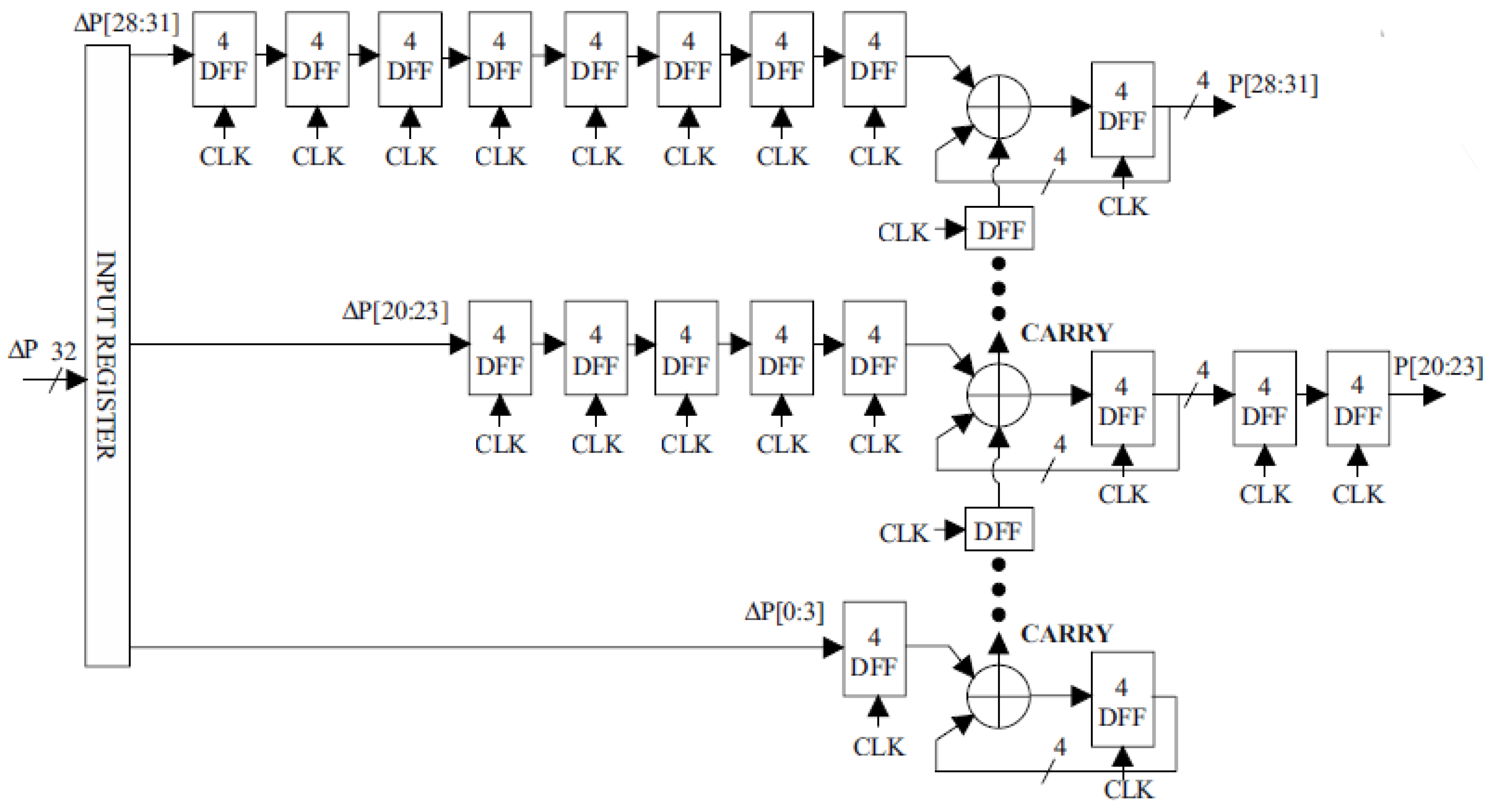
In [
2], it is proposed to reduce the dependence of the delay in the propagation of transfer signals, operands and transfer signals must be captured in constant states by D-triggers. In the case of the use of four-bit kernels, the structural scheme of such a phase accumulator will come in the following for
Figure 1.
To maintain the correct state of the accumulator, during the implementation time of the addition, it is necessary to maintain the value of the phase word at the input of the circuit. The accumulation result will appear on the accumulator’s outlet only after a certain number of cycles. For example, in
Figure 1 it will be nine full clock cycles. In addition, for a 32-bit accumulator with a four-bit conveyor, the circuit requires 144 D-triggers, which is a clear synchronization. This is a separate complex scientific and application task. To simplify the scheme and reduce the number of D flip-flops, carry schemes are used the delay registers. The fee for this simplification is to reduce the frequency of updating trigger states only
. The phase word coming to the phase accumulator is in the most cases formed in circuits with much lower performance, and often asynchronously to the reference DDS source.
In order to allow asynchronous loading of the input phase word, it is necessary to further use double buffering of the phase-accumulator input. Output elements of the delay are constructed similarly to the input, so that the least significant bits are received with the greatest delay, and the most important bits are received with a minimal delay. In
Figure 1 data of the most significant 12 bits of the phase accumulator are delayed in the conveyor registers to achieve full synchronization in the phase-amplitude converter.
The simplicity of the structure of such a phase accumulator is achieved by reducing the number of delay registers in less significant bits. It becomes possible because only the most significant bits from the phase accumulator output are used to convert the phase counters into a sinusoidal function. The delay between the occurrence of the actual value of the phase at the output and the loading of the input phase word will be nine full clock cycles.
2. Proposed Method
As has been researched in [
3,
4,
5,
6,
7,
8,
9,
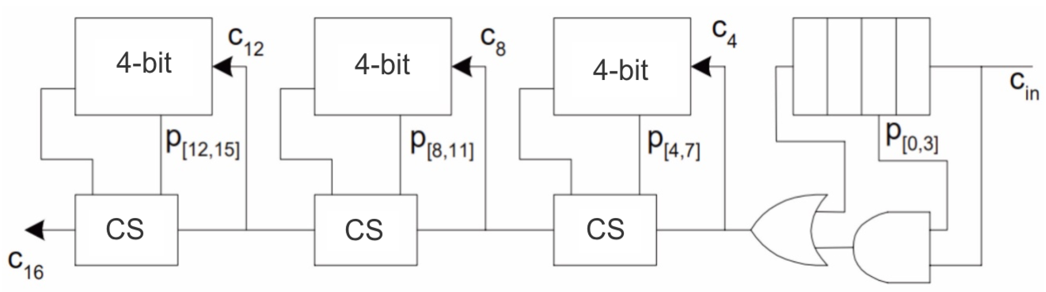
10], the most promising adders for the use in the core of the synthesizer direct digital synthesis are the carry–save adders (CSA). Therefore, we considered two main types of CSA adders—one with a transport delay and a fixed block length; and the other with a transport delay and a variable length of the block in more detail, see
Figure 2.
The greatest delay arose when the transfer signal was generated in the 0th stage of the least significant block, passing through the other three cascades of the block, then entering the element OR. Next, the transfer signal passed through 2 transfer passes, and then through three of the four stages of the most significant block.
Thus, for a
k-bit adder with a block size b, the delay of the transfer signal was determined by the Equation (
1).
where
is time of propagation of the carry signal through one cascade of the adder (from
to
),
is time delay in passing the carry signal through the transfer passage circuit, and
D is time signal delay time on an OR circuit.
Suppose that
in a standard RCA (Ripple-Carry Adder) compiler, based on two half-adders. Delay
occurred case that the carry block is based on the logical elements AND and OR. Accordingly, we obtain:
Optimal block size,
, can be found by differentiating the right side of the expression (
2) with the transfer
b and equating the result to zero
Accordingly, the optimal block size was determined by Equation (
3).
Based on this, the delay of the adder was:
Consider the alternative variant [
11,
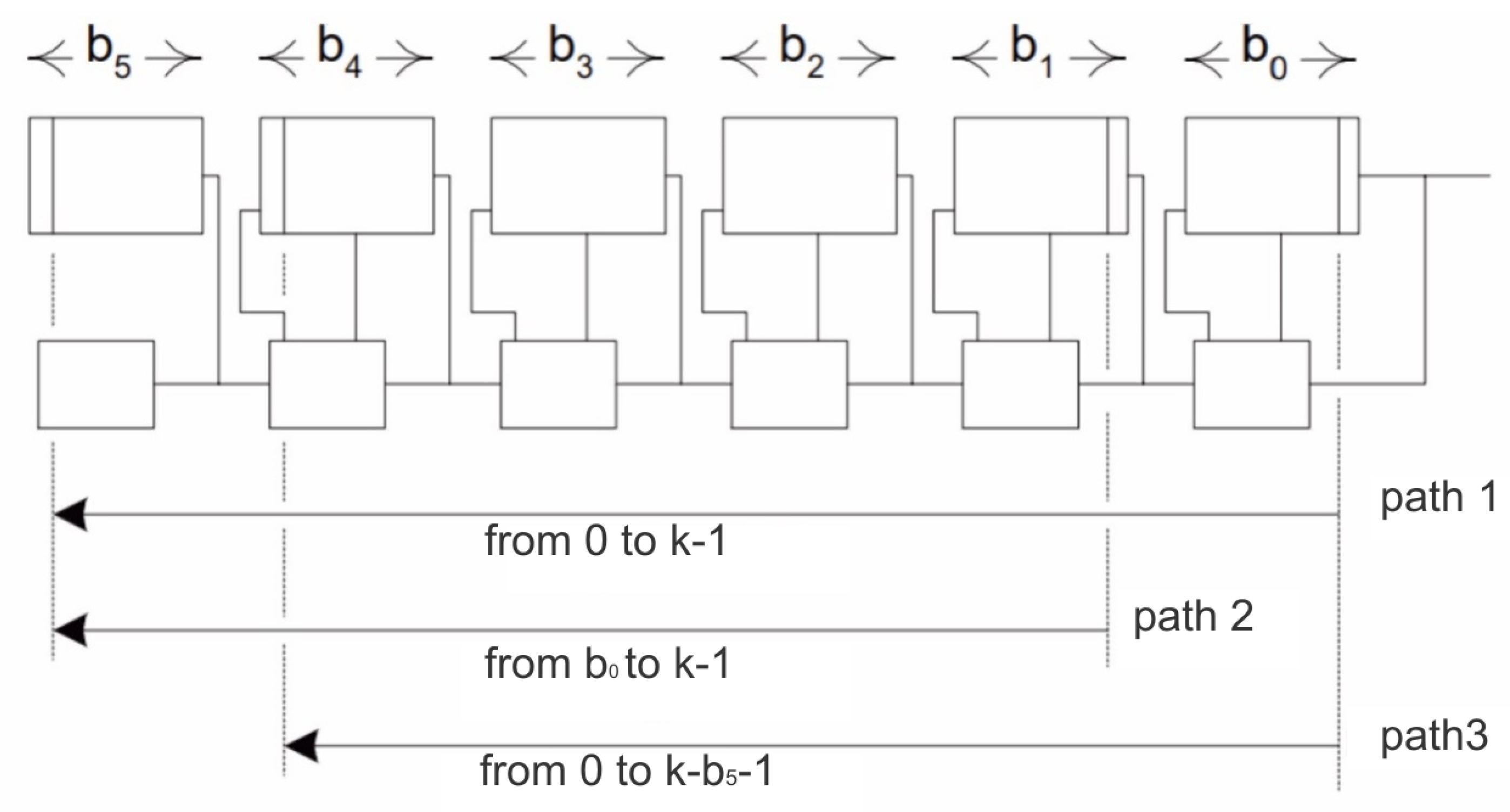
12] of the adder with the transmission delay signal with the variable length of the block (TCSA-V). Consider the adder with t blocks transfer passes with dimensions
, which are located from left to right (
Figure 3).
Consider the equation for the worst case delay of the transfer signal from the cascade 0 to the cascade
, which corresponds to the path 1 of the diagram in
Figure 3:
Consider the transfer generated by the cascade
, the extreme right block 1 and passes along path 2 from the leftmost left-hand side of the adder. This delay is determined by Equation (
4).
Case
, when
maybe 1 more
without deteriorating path delay compared to path 1. Similarly, if
to cascade
the worst value of the delay from the cascade
was no greater than the delay of the path 1. Blocks located on the right side of the adder may have dimensions of a simple incremental sequence [
13]. Now consider the transfer generated in step 0 and used at the extreme left end of the penultimate blocker adder, at stage
. This corresponds to the path 3 of the diagram in the
Figure 3. This delay was determined by Equation (
5).
In case
, block size
may be larger than the block size
without increasing the delay compared to the path 1. Blocks to the left of the center of the adder can had dimensions as those form a simple incremental sequence. The longest delay in the transfer signal occurred in the adder with a variable length of the block:
The optimal number of blocks was determined by the Equations (
7)–(
9).
which was about at
times less than the adder with a fixed block size. Consequently, based on the analysis of the main types of adder that can be used in direct digital frequency synthesizers, it has been established that the adder with a blocked signal transmitted with a variable length of the block (TCSA-V Adder) had a lower delayed synthesized signal compared to the TCSA-F Adder. Presented mathematical models of adders with a fixed and variational block size indicate that the adder with the variable size of the transfer pass block was faster than other types of parallel adders working in the classical digital basis [
14]. It was necessary to check that the use of shift-by-spaced shifters with a variational block in the core of a direct digital synthesizer allowed the development of fast DDS with a lower delay, and therefore with a higher maximum output frequency, as compared to other types of adder.
To confirm this thesis, an experimental layout of the DDS synthesizer was developed for conducting comparative studies of phase accumulators on a sequential conveyor, a transfer conveyor with a fixed transfer passage block, and a transfer conveyor with a variable transfer block.
3. Experimental Part
The purpose of the experimental layout was to study the characteristics of various types of synthesizers of direct synthesis. Therefore, its tactical characteristics were as follows:
Easy to implement and repeat;
Using standard components;
Ability to expand the functionality;
Ability and ease of reprogramming the synthesizer;
A clear user interface.
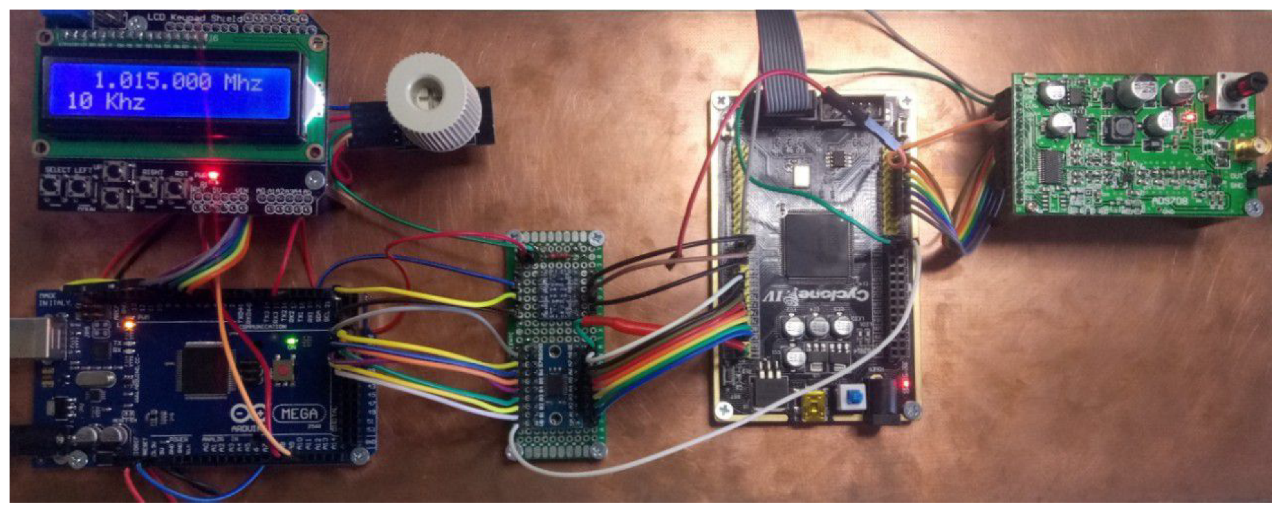
To simplify the design and implementation of the experimental layout, a modular design was used. That is, instead of placing all the components on a single printed circuit board, we used separate ready modules [
15]. The basis of the layout was a two-level synthesizer module, which ensured the formation of the code of the amplitude of the output signal. The output analog signal generated a DAC module at the input of which the amplitude codes from the DDS module are fed [
16]. In order to control the frequency of the synthesizer, as well as to display information about the current output frequency and synthesizer state, a direct digital synthesizer experimental layout control system was designed. The block diagram of the experimental layout is shown in
Figure 4.
As a synthesizer of direct synthesis, it was decided that we should use a chip programmable logic with a reprogrammed structure of DDS synthesizers on adders of different types. The field-programmable gate array (FPGA) module was based on the EP4CE6E22C8 chip of the Altera Cyclone IV family. The EP4CE6E22C8 had a total of 6272 logical elements, embedded 270 kb memory, two general-purpose PLLs (Phase-Locked Loop), a chip supporting up to 10 global clock signals, and supported up to 179 user input/output ports [
17].
Everything necessary for the operation of the FPGA was mounted on the motherboard. The card could be controlled with the help of two buttons; a separate reset button was present. The FPGA was clocked using a clock generator and the clock frequency was 50 MHz. For communication with other devices, other than I/O ports, the micro USB connector was mounted on the board. Firmware and software debugging were performed using two blocks with JTAG (Joint Test Action Group) and as output interfaces. Thus, the chosen FPGA module fully corresponded to the given tactical and technical characteristics, providing both high functionality and ease of operation. In the DDS synthesizer, an important component was the output DAC, which ensured the correctness of converting the digital code into amplitude values. And its quality largely determines the bandwidth of the output signal, frequency response and phase response.
The basis of the output DAC synthesizer DDS was the chip AD9708, which is an eight-bit parallel dual-to-analog converter. In addition to the AD9708, we installed on the motherboard a voltage regulator 3.3 V AMS11117, a Butterworth filter for two AD8047 operating amplifiers, and an alternating resistor for adjusting the amplitude of the output signal.
The board was powered by a voltage of 5 V. The output connector used high-frequency separation type SMA (SubMiniature version A). The module provided 10 V (−5 V, +5 V) signal output. The cutoff frequency of the output LPF (Low-Pass Filter) was 40 MHz.
The AD9708 is an eight-bit parallel DAC from the TxDAC series of high-performance, low-power analogue digital converters. The operating range of the supply voltage is from +2.7 V to +5.5 V. The AD9708 is manufactured using the advanced CMOS process. The chip has an internal source of reference voltage U = 1.2 V, and the output voltage corresponds to 1.25 V. The AD9708 can be driven by different external reference voltages. The output current of the AD9708 can be adjusted in the range from 2 mA to 20 mA, without any deterioration in the dynamic characteristics.
As shown above, the delay in the transfer signal in the combiner of the core of the direct digital synthesizer is one of the factors limiting the maximum output frequency of the synthesizer. The purpose of this comparative study is to determine the fastest adder, which can be used in the core of the direct digital synthesizer.
We investigated the delay time in three types of adder: a parallel adder with a sequential transfer, a parallel adder with a fixed transfer delay, a parallel adder with a variational transfer delay. For this purpose, schemes of adders were developed in the environment of the Quartus Prime 13.1 firm Altera.
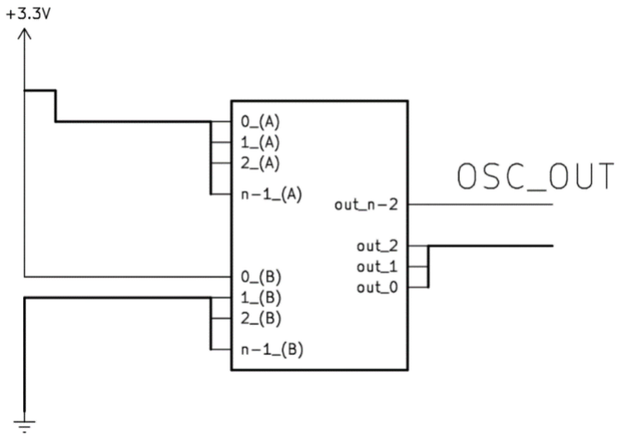
The research was carried out on adders at a digit of eight, 16, 32, 64 bits. As is known, the greatest delay in the propagation of the transfer signal occurred when it occurred in the LSB (Least Significant Bit). For example, in the case of an eight-bit adder, the appearance of the transfer in the LSB bit will occur provided: 11111111 + 00000001 = [1] 00000000. To reproduce this condition, one adder input was connected to the 3.3 V power supply line, the other to the GND line, except the LSB connected to line 3.3 V (
Figure 5).
To fix the delay, a two-channel digital oscilloscope Siglent SDS1202X-E was used, one channel connected to the output of the LSB of B, the other to the OSC_OUT output, which was the output of the MSB (Most Significant Bit). The clock speed of Cyclone IV was 50 MHz.
RCA adders were investigated, that is, parallel adders with sequential transfer. The eight-bit RCA add-on model was included in the standard Quartus Prime 13.1 component library, so it was chosen as the base component, based on which all other model models with sequential transport were built.
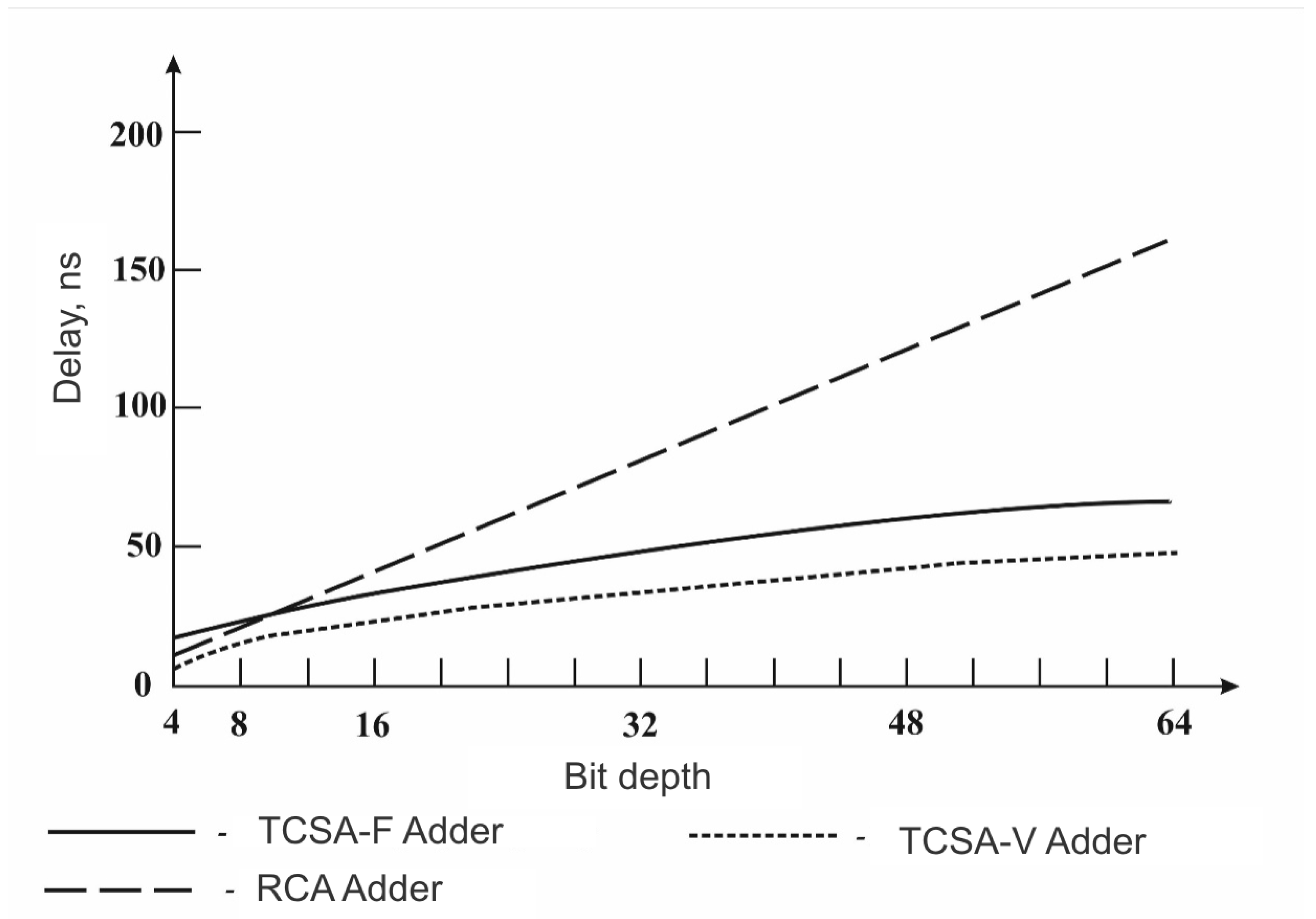
As expected, the slowest was an adder with a sequential transfer, and the delay of the transfer signal varied linearly with the increase of the adder’s bit, see
Table 1. A 64-bit RCA adder had a delay of a transfer signal of 7.65 times greater than the eight-bit and almost two-times that of a 32-bit. Thus, the RCA large-volume adder was not desirable to use in the synthesizer’s core.
Transfer delayed summers were faster than the RCA adder, and the dependence of the delay of the transfer signal on the bit in them was nonlinear. For a 64-bit CSA adder with a fixed length of the block, the delay of the transfer signal was 2.86 times greater than the eight-bit and 1.4 times that of the 32-bit. A 64-bit CSA adder with a variable-length block is slower than eight-bit in 3.2 times, and from 32-bit—1.4-fold. Comparison of a CSA adder with a fixed block length and a variable block length has been done and the results are presented in
Table 2.
On average, the adder with variable length of the block was 1.44 times faster than the adder with a fixed length of the block. In the case of 32-bit adder, the ratio of TRCA/TCSA-V, that is, the delay time relations for the RCA and CSA-V adders were equal: 80.5/33.6 = 2.4. That is, a 32-bit parallel adder and a sequential transfer of 2.4 times slower than a parallel adder with a transport delay with variable-length block.
The advantage of a parallel adder with a variable block length was that with increasing digit, the delay time grew significantly less than in a sequential transfer adder, so it was well suited for use in the core of the synthesizer. However, as the bit rate increased, the complexity of designing such an adder increased, including the definition of optimal configuring the lengths of the blocks. Thus, the transfer adder with the variable transfer pass was faster than other types of classical adders, see
Figure 6.
The delay of the transfer signal in the synthesizer was one of the critical factors for determining the maximum output frequency of the synthesizer, we can say that there was a direct proportional relationship between these two quantities.
In addition, an experiment was conducted to determine the maximum output frequency with the use of three types of 32-bit adders in the synthesizer core: a parallel adder with a sequential transfer, a parallel adder with a transport delay and a fixed block length, and a parallel adjunct with a transport delay with a variational size of the transfer passage block. It was established that the maximum achievable frequency without distortion in the dynamic range of the DAC was 1.7 MHz for a synthesizer with a sequential transfer adder, 2.8 MHz for a synthesizer with a transfer admission with a fixed block length, and 4.08 MHz for the synthesizer with the adder with a transport delay with variation in block length.
4. Results and Discussion
The paper deals with the problems of delayed transfer signals in the DDS phase accumulator adders. Transfer delay is one of the factors that affects the maximum output frequency of the DDS synthesizer. The main types of adders used in DDS synthesizers are described. Separately, attention was paid to the adder with a consistent transfer of the transfer signal, adders with a transmission signal transmission with a fixed block length, adders with a signal transmission delay with a variable block length, and a mathematical analysis of the origin and duration of the delay of the transfer signal in them.
The experimental model of the synthesizer with direct digital synthesis was designed and built, its structural and principal scheme were developed, and the choice of used components was grounded. The software for experimental layout management system was developed. We designed eight, 16, 32 and 64 bit adder models of RCA, CSA-F, CSA-V in the Quartus Prime 13.1 software schematic editor.
The experimental determination of the delay of the transfer signal in the three types of adder of different discharges was carried out. It was determined that the fastest among the investigated adders was an adder with a transport delay with a variational block, and, with the increase in the adder’s bit, the delay of the transfer signal increased by only 3.19 times, compared with 7.65 times in the case of a sequential transfer adder. On average, the adder with variable length of the block is faster than the adder with a fixed length of the block in 1.43 times, in 2.4 times as a adder with a sequential transfer.
The maximum output frequency without distortion in the dynamic range of the DAC was determined with the use of a 32-bit adder and a fixed clock frequency of 50 MHz. For RCA, it was 1.7 MHz, for CSA-F it was 2.8 MHz, and for CSA-V it was 4.08 MHz. So the use of CSA-V in comparison with RCA will allow you to increase the maximum clock frequency by 2 times.
5. Conclusions
It was found that the use of an adder with a variable length of a block in the core of a direct digital synthesizer would increase the maximum output frequency by 2.4 times compared to the adder with a parallel transfer, and by 1.43 times as compared with the adder with a fixed length the block. The results of the practical research of direct digital frequency synthesizers presented in this paper give us a new direction in the research of systems of digital synthesis frequencies and signals the direction of improving the internal structure of digital synthesis systems by choosing the optimal structure of the functional elements of the synthesizer. Also, from the work it is visible that as the number of adders grows, and the delay of the considered adders increases as they are constructed in a sequential scheme. In the synthesis of high frequencies, as is the case in mobile communication systems, radar systems, measuring devices, it is important to minimize the delay of the synthesized signal. Therefore, a promising area of research is the application of non-positional numerical systems for the construction of frequency synthesizers and signals with minimal delay of the output signal.
In further research it is necessary to analyze the levels of phase and amplitude noise of DDS synthesizers with phase accumulators built on different types of arithmetic. It is also necessary to compare the speed characteristics of DDS synthesizers constructed in binary [
18] and RNS [
19] systems.


