A Review of Current Methods in Microfluidic Device Fabrication and Future Commercialization Prospects

 , , , and
Abstract
1. Introduction
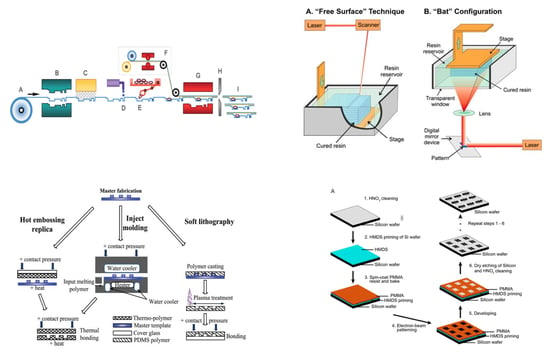
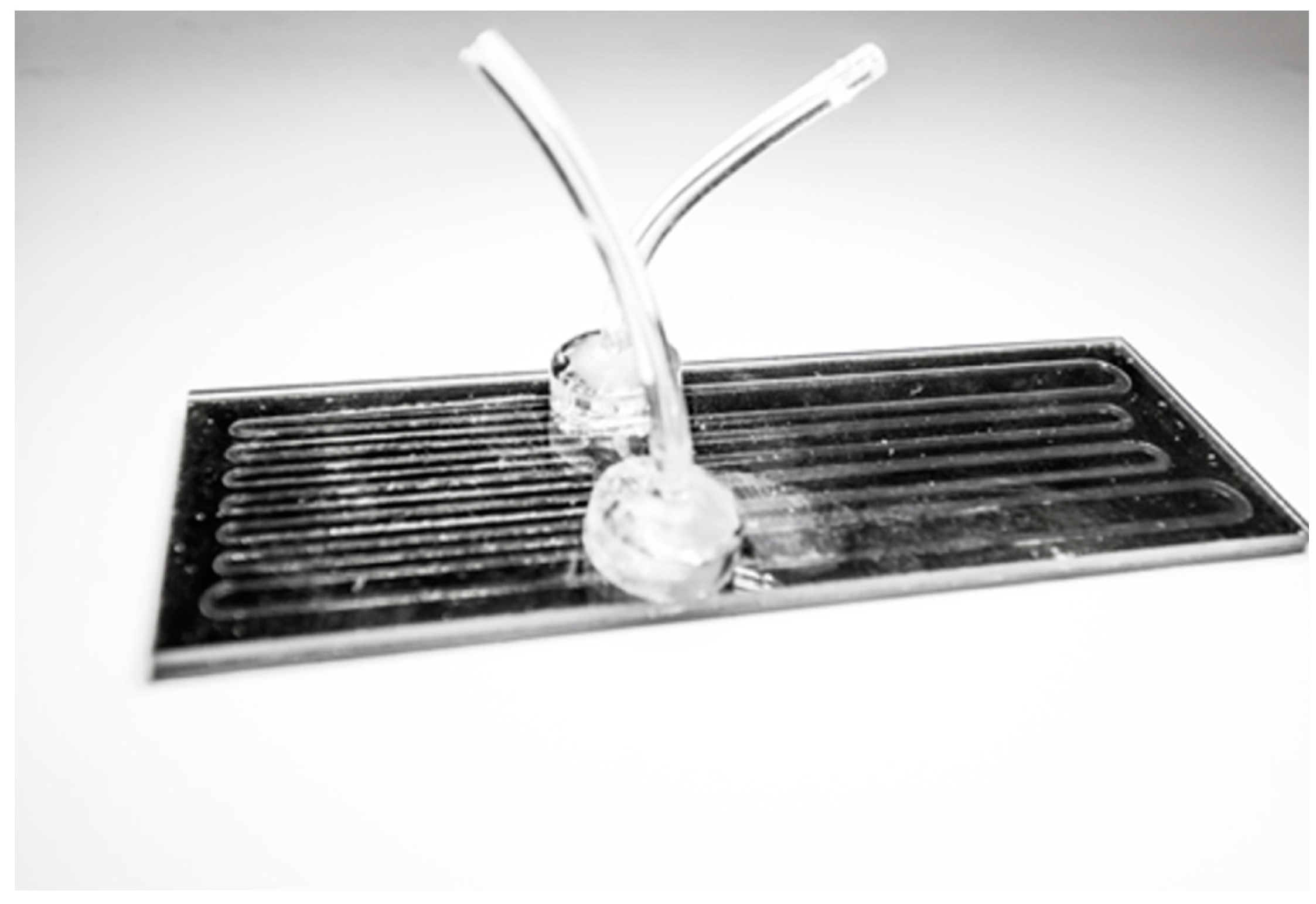
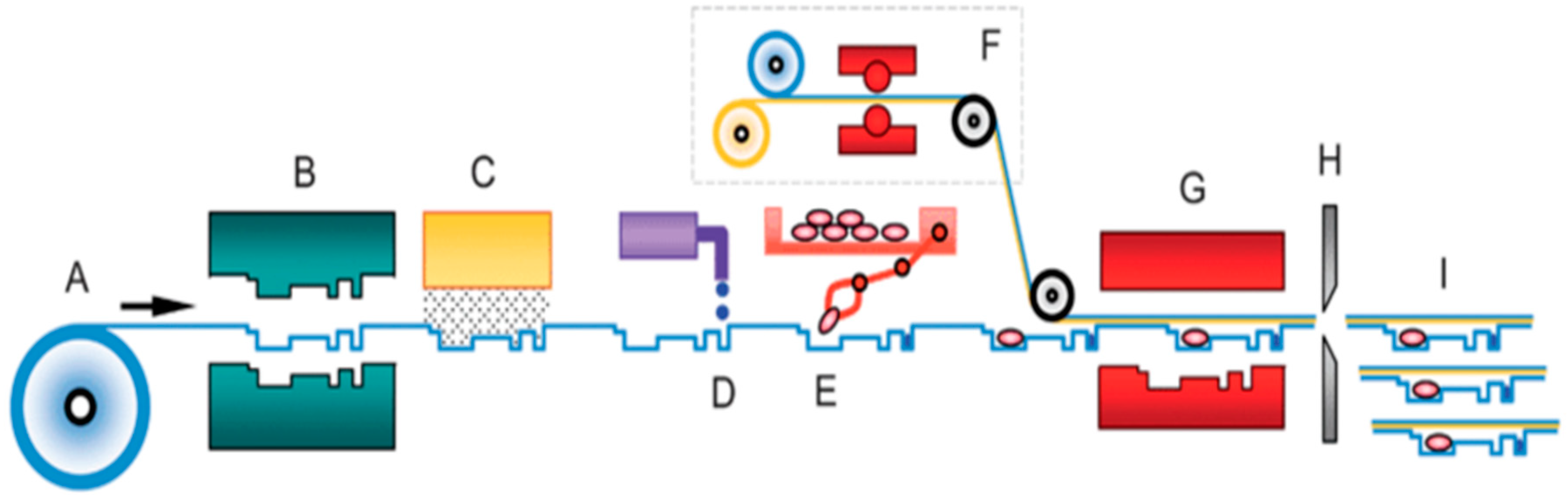
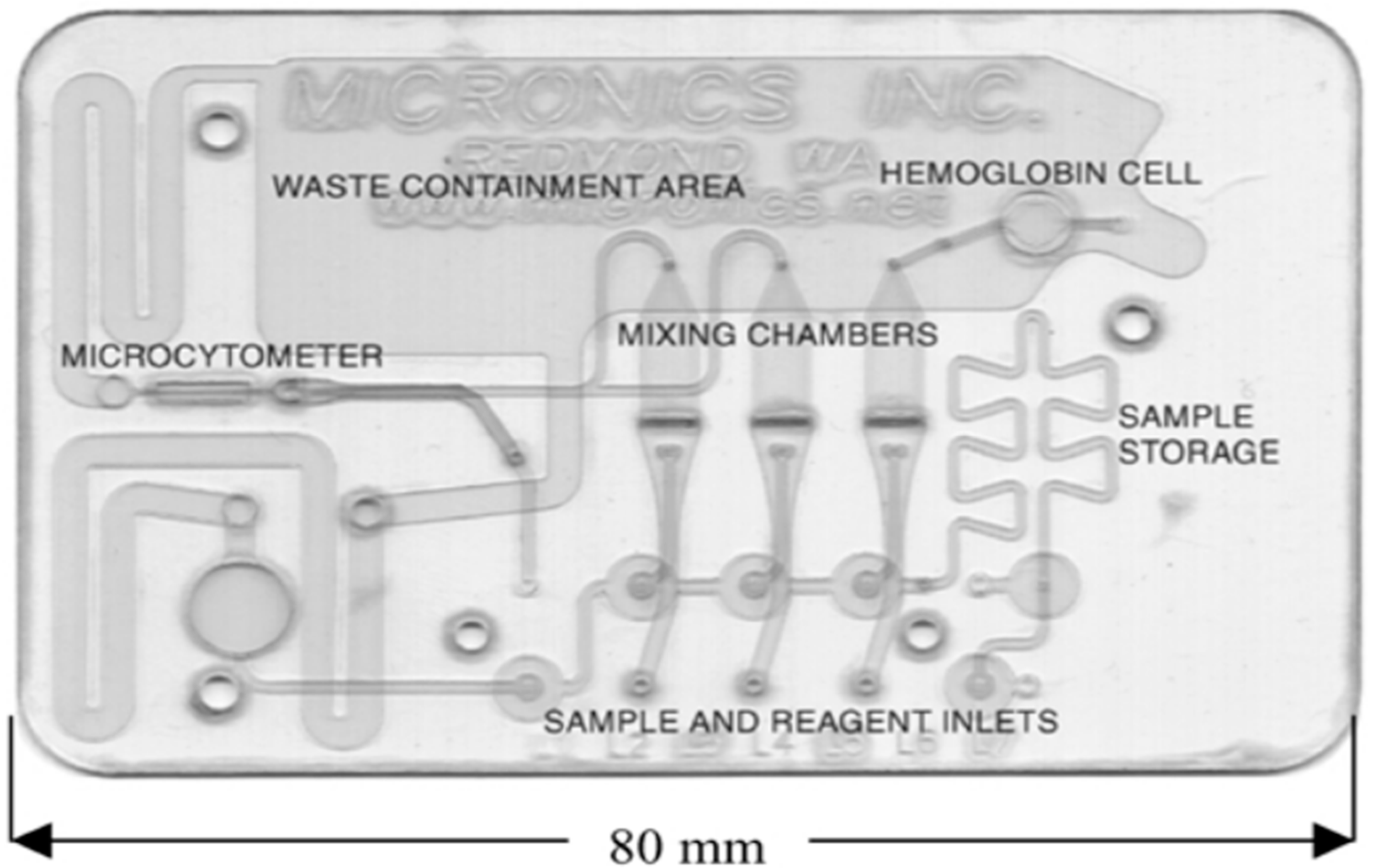
2. Laminates
3. Molding
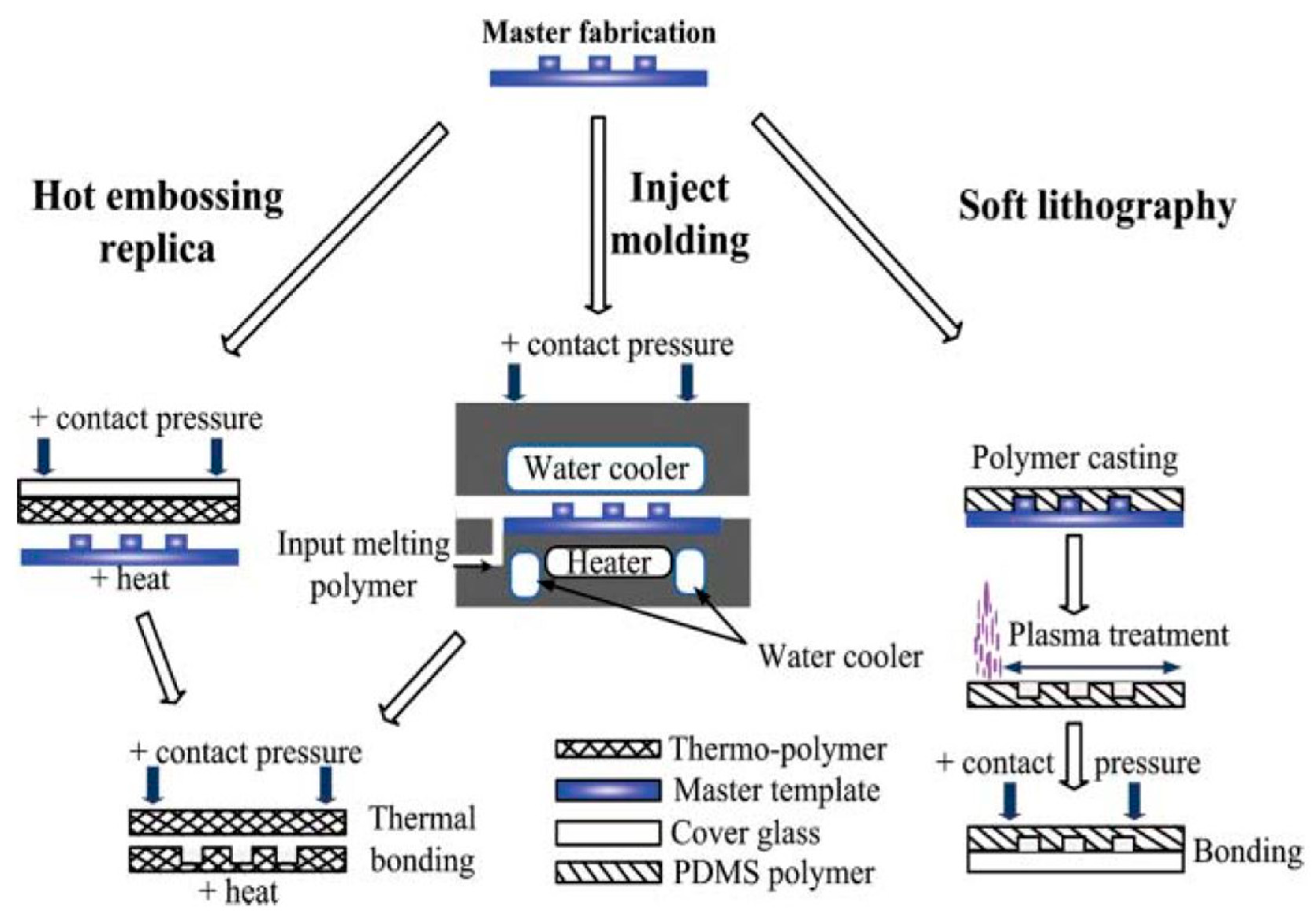
3.1. Replica Molding
3.2. Injection Molding
3.3. Hot Embossing
4. 3D Printing
4.1. Fused Deposition Molding
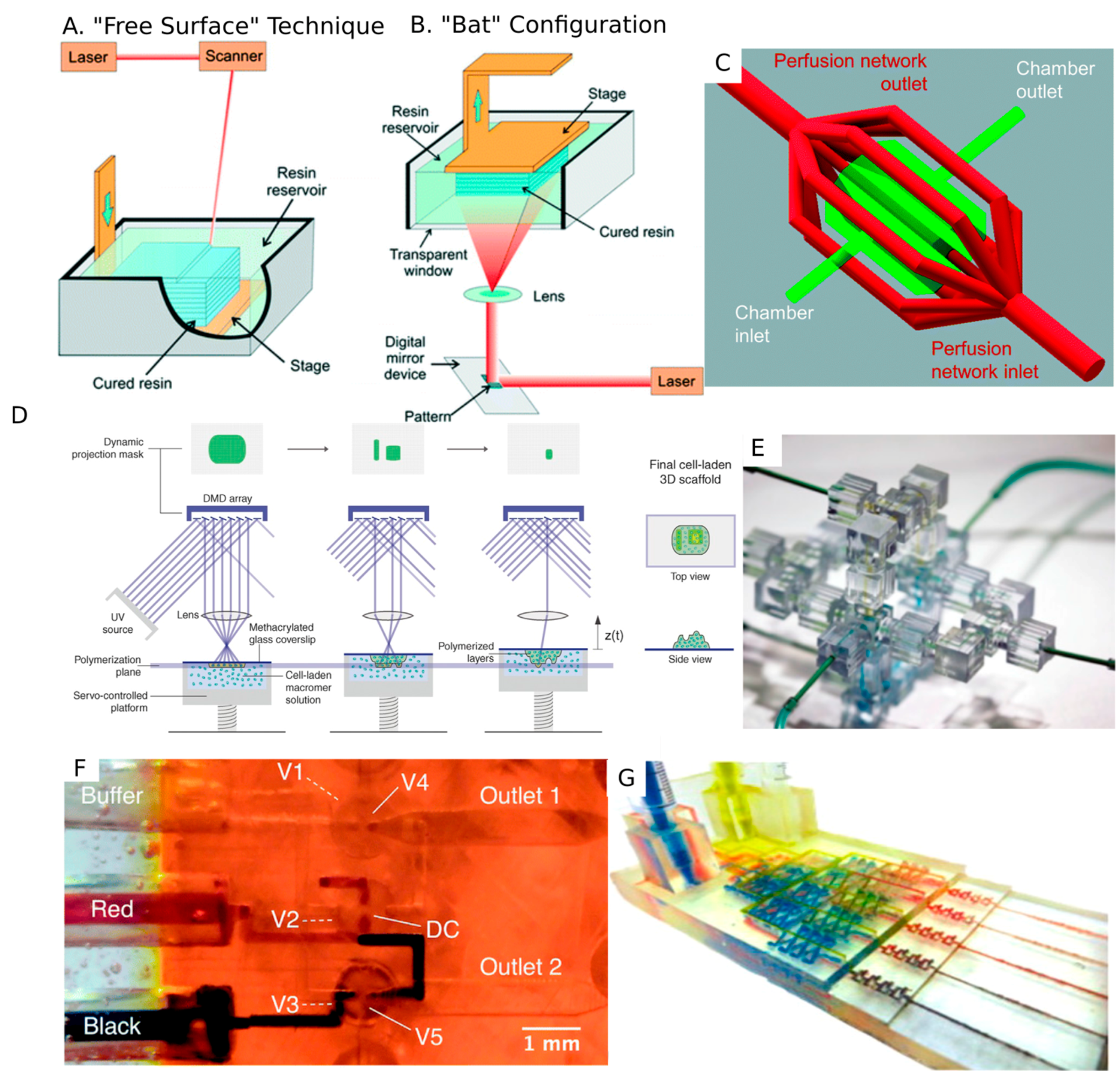
4.2. Stereolithography
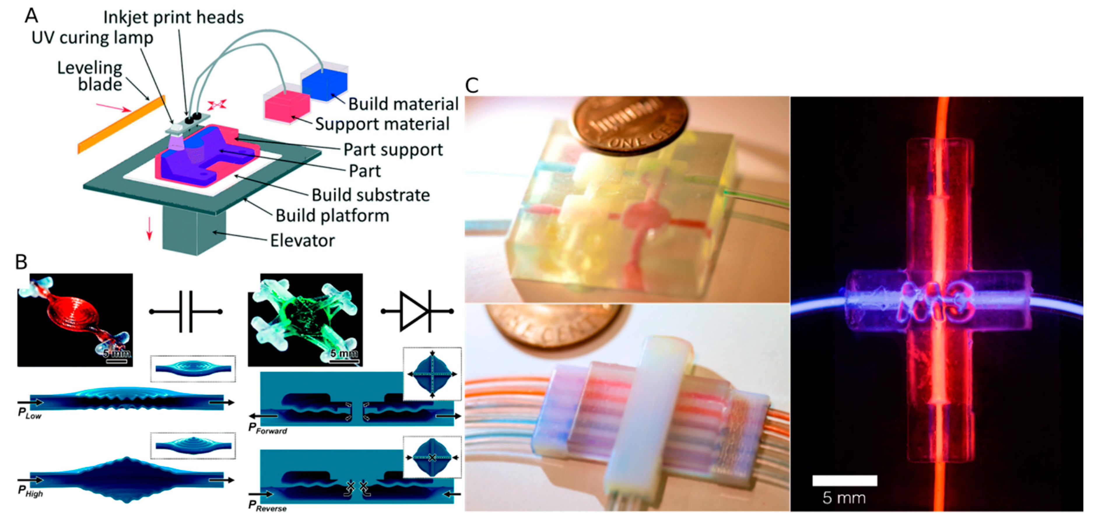
4.3. Multi Jet Modeling
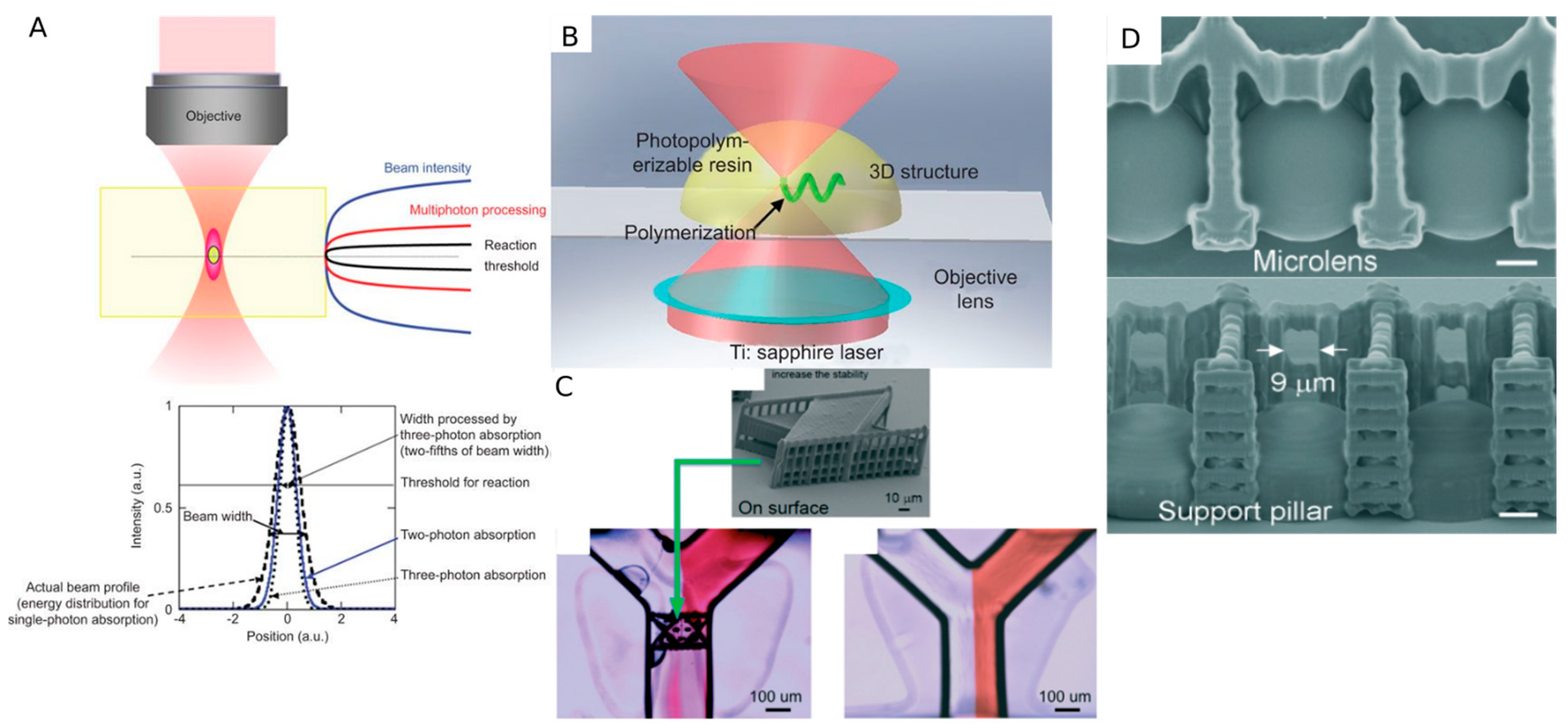
4.4. Two-Photon Polymerization
5. Nanofabrication
5.1. Extreme Ultraviolet Lithography
5.2. Electron Beam Lithography
5.3. Nanoimprint Lithography
5.4. Anodic Aluminum Oxidation
6. Conclusions
Author Contributions
Funding
Acknowledgments
Conflicts of Interest
References
- Hansen, C.L.; Skordalakes, E.; Berger, J.M.; Quake, S.R. A robust and scalable microfluidic metering method that allows protein crystal growth by free interface diffusion. Proc. Natl. Acad. Sci. USA 2002, 99, 16531–16536. [Google Scholar] [CrossRef] [PubMed]
- Takayama, S.; Ostuni, E.; LeDuc, P.; Naruse, K.; Ingber, D.E.; Whitesides, G.M. Subcellular positioning of small molecules. Nature 2001, 411, 1016. [Google Scholar] [CrossRef] [PubMed]
- Son, J.; Samuel, R.; Gale, B.K.; Carrell, D.T.; Hotaling, J.M. Separation of sperm cells from samples containing high concentrations of white blood cells using a spiral channel. Biomicrofluidics 2017, 11, 054106. [Google Scholar] [CrossRef] [PubMed]
- Jafek, A.R.; Harbertson, S.; Brady, H.; Samuel, R.; Gale, B.K. Instrumentation for xPCR Incorporating qPCR and HRMA. Anal. Chem. 2018, 90, 7190–7196. [Google Scholar] [CrossRef] [PubMed]
- Bange, A.; Halsall, H.B.; Heineman, W.R. Microfluidic immunosensor systems. Biosens. Bioelectron. 2005, 20, 2488–2503. [Google Scholar] [CrossRef] [PubMed]
- Safdar, M.; Jänis, J.; Sánchez, S. Microfluidic fuel cells for energy generation. Lab Chip 2016, 16, 2754–2758. [Google Scholar] [CrossRef] [PubMed]
- Guo, M.T.; Rotem, A.; Heyman, J.A.; Weitz, D.A. Droplet microfluidics for high-throughput biological assays. Lab Chip 2012, 12, 2146. [Google Scholar] [CrossRef] [PubMed]
- Xia, Y.; Whitesides, G.M. SOFT LITHOGRAPHY. Annu. Rev. Mater. Sci. 1998, 28, 153–184. [Google Scholar] [CrossRef]
- McDonald, J.C.; Duffy, D.C.; Anderson, J.R.; Chiu, D.T.; Wu, H.; Schueller, O.J.; Whitesides, G.M. Fabrication of microfluidic systems in poly(dimethylsiloxane). Electrophoresis 2000, 21, 27–40. [Google Scholar] [CrossRef]
- Kim, P.; Kwon, K.W.; Park, M.C.; Lee, S.H.; Kim, S.M. Soft Lithography for Microfluidics: A Review. Biochip J. 2008, 2, 1–11. [Google Scholar]
- Qin, D.; Xia, Y.; Whitesides, G.M. Soft lithography for micro- and nanoscale patterning. Nat. Protoc. 2010, 5, 491–502. [Google Scholar] [CrossRef] [PubMed]
- Faustino, V.; Catarino, S.O.; Lima, R.; Minas, G. Biomedical microfluidic devices by using low-cost fabrication techniques: A review. J. Biomech. 2016, 49, 2280–2292. [Google Scholar] [CrossRef] [PubMed]
- Xia, Y.; Si, J.; Li, Z. Fabrication techniques for microfluidic paper-based analytical devices and their applications for biological testing: A review. Biosens. Bioelectron. 2016, 77, 774–789. [Google Scholar] [CrossRef] [PubMed]
- Walsh, D.I.; Kong, D.S.; Murthy, S.K.; Carr, P.A. Enabling Microfluidics: from Clean Rooms to Makerspaces. Trends Biotechnol. 2017, 35, 383–392. [Google Scholar] [CrossRef] [PubMed]
- Ontiveros, F.; Mcdowell, J.R. Ultra-Thin Microfluidic Devices Built via Thermal Lamination; Biology Faculty Publications, Paper 28; St. John Fisher College: Rochester, NY, USA, 2016. [Google Scholar]
- Nath, P.; Fung, D.; Kunde, Y.A.; Zeytun, A.; Branch, B.; Goddard, G. Rapid prototyping of robust and versatile microfluidic components using adhesive transfer tapes. Lab Chip 2010, 10, 2286. [Google Scholar] [CrossRef] [PubMed]
- Kinahan, D.J.; Julius, L.A. N.; Schoen, C.; Dreo, T.; Ducrée, J. Automated Dna Purification and Multiplexed Lamp Assay Preparation on a Centrifugal Microfluidic “ Lab -on-a- Disc ” Platform. In Proceedings of the 2018 IEEE Micro Electro Mechanical Systems (MEMS) Belfast, UK, 21–25 January 2018; pp. 1134–1137. [Google Scholar]
- Mahmud, M.; Blondeel, E.; Kaddoura, M.; MacDonald, B. Features in Microfluidic Paper-Based Devices Made by Laser Cutting: How Small Can They Be? Micromachines 2018, 9, 220. [Google Scholar] [CrossRef]
- Serra, M.; Pereiro, I.; Yamada, A.; Viovy, J.-L.; Descroix, S.; Ferraro, D. A simple and low-cost chip bonding solution for high pressure, high temperature and biological applications. Lab Chip 2017, 17, 629–634. [Google Scholar] [CrossRef] [PubMed]
- Focke, M.; Kosse, D.; Müller, C.; Reinecke, H.; Zengerle, R.; von Stetten, F. Lab-on-a-Foil: Microfluidics on thin and flexible films. Lab Chip 2010, 10, 1365. [Google Scholar] [CrossRef] [PubMed]
- Romanov, V.; McCullough, J.; Gale, B.; Frost, A. Nanoemulsions. Unpublished work. 2018. [Google Scholar]
- Martin, P.M.; Matson, D.W.; Bennett, W.D.; Lin, Y.; Hammerstrom, D.J. Laminated plastic microfluidic components for biological and chemical systems. J. Vac. Sci. Technol. A Vac. Surf. Film 1999, 17, 2264–2269. [Google Scholar] [CrossRef]
- Weigl, B.H.; Bardell, R.; Schulte, T.; Battrell, F.; Hayenga, J. Design and Rapid Prototyping of Thin-Film Laminate-Based Microfluidic Devices. Circuit Des. 2001, 267–274. [Google Scholar]
- Wu, J.; Gu, M. Microfluidic sensing: State of the art fabrication and detection techniques. J. Biomed. Opt. 2011, 16, 080901. [Google Scholar] [CrossRef] [PubMed]
- Pinto, V.C.; Sousa, P.J.; Cardoso, V.F.; Minas, G. Optimized SU-8 processing for low-cost microstructures fabrication without cleanroom facilities. Micromachines 2014, 5, 738–755. [Google Scholar] [CrossRef]
- Li, Z.; Gu, Y.; Wang, L.; Ge, H.; Wu, W.; Xia, Q.; Yuan, C.; Chen, Y.; Cui, B.; Williams, R.S. Hybrid Nanoimprint—Soft Lithography with Sub-15 nm Resolution 2009. Nano Lett. 2009, 9, 2306–2310. [Google Scholar] [CrossRef] [PubMed]
- Yang, Y.; Kulangara, K.; Sia, J.; Wang, L.; Leong, K.W. Engineering of a microfluidic cell culture platform embedded with nanoscale features. Lab Chip 2011, 11, 1638–1646. [Google Scholar] [CrossRef] [PubMed]
- Ugolini, G.S.; Visone, R.; Redaelli, A.; Moretti, M.; Rasponi, M. Generating Multicompartmental 3D Biological Constructs Interfaced through Sequential Injections in Microfluidic Devices. Adv. Healthc. Mater. 2017, 6. [Google Scholar] [CrossRef] [PubMed]
- Sticker, D.; Rothbauer, M.; Lechner, S.; Hehenberger, M.T.; Ertl, P. Multi-layered, membrane-integrated microfluidics based on replica molding of a thiol-ene epoxy thermoset for organ-on-a-chip applications. Lab Chip 2015, 15, 4542–4554. [Google Scholar] [CrossRef] [PubMed]
- Giboz, J.; Copponnex, T.; Mélé, P. Microinjection molding of thermoplastic polymers: A review. J. Micromech. Microeng. 2007, 17. [Google Scholar] [CrossRef]
- Wiedemeier, S.; Römer, R.; Wächter, S.; Staps, U.; Kolbe, C.; Gastrock, G. Precision moulding of biomimetic disposable chips for droplet-based applications. Microfluid. Nanofluidics 2017, 21, 1–11. [Google Scholar] [CrossRef]
- Szydzik, C.; Gavela, A.F.; Herranz, S.; Roccisano, J.; Knoerzer, M.; Thurgood, P.; Khoshmanesh, K.; Mitchell, A.; Lechuga, L.M. An automated optofluidic biosensor platform combining interferometric sensors and injection moulded microfluidics. Lab Chip 2017, 17, 2793–2804. [Google Scholar] [CrossRef] [PubMed]
- Vereshchagina, E.; Andreassen, E.; Gaarder, R.; Mielnik, M.M. Synergy of 3D Printing and Injection Molding: A New Prototyping Method for Rapid Design Optimization and Manufacturing of Microfluidic Devices. In Proceedings of the µTAS 2017 Conference, Savannah, GA, USA, 22–26 October 2017. [Google Scholar]
- Lin, T.Y.; Do, T.; Kwon, P.; Lillehoj, P.B. 3D printed metal molds for hot embossing plastic microfluidic devices. Lab Chip 2017, 17, 241–247. [Google Scholar] [CrossRef] [PubMed]
- Weerakoon-Ratnayake, K.M.; O’Neil, C.E.; Uba, F.I.; Soper, S.A. Thermoplastic nanofluidic devices for biomedical applications. Lab Chip 2017, 17, 362–381. [Google Scholar] [CrossRef] [PubMed]
- Heckele, M.; Schomburg, W.K. Review on micro molding of thermoplastic polymers. J. Micromech. Microeng. 2004, 14. [Google Scholar] [CrossRef]
- Bocquet, L.; Tabeling, P. Physics and technological aspects of nanofluidics. Lab Chip 2014, 14, 3143–3158. [Google Scholar] [CrossRef] [PubMed]
- Debono, M.; Voicu, D.; Pousti, M.; Safdar, M.; Young, R.; Kumacheva, E.; Greener, J. One-step fabrication of microchannels with integrated three dimensional features by hot intrusion embossing. Sensors 2016, 16, 2023. [Google Scholar] [CrossRef] [PubMed]
- Au, A.K.; Huynh, W.; Horowitz, L.F.; Folch, A. 3D-Printed Microfluidics. Angew. Chem. Int. Ed. 2016, 55, 3862–3881. [Google Scholar] [CrossRef] [PubMed]
- Waheed, S.; Cabot, J.M.; Macdonald, N.P.; Lewis, T.; Guijt, R.M.; Paull, B.; Breadmore, M.C. 3D printed microfluidic devices: Enablers and barriers. Lab Chip 2016, 16, 1993–2013. [Google Scholar] [CrossRef] [PubMed]
- McDonald, J.C.; Chabinyc, M.L.; Metallo, S.J.; Anderson, J.R.; Stroock, A.D.; Whitesides, G.M. Prototyping of microfluidic devices in poly(dimethylsiloxane) using solid-object printing. Anal. Chem. 2002, 74, 1537–1545. [Google Scholar] [CrossRef] [PubMed]
- Bhattacharjee, N.; Urrios, A.; Kang, S.; Folch, A. The upcoming 3D-printing revolution in microfluidics. Lab Chip 2016, 16, 1720–1742. [Google Scholar] [CrossRef] [PubMed]
- Moore, J.L.; McCuiston, A.; Mittendorf, I.; Ottway, R.; Johnson, R.D. Behavior of capillary valves in centrifugal microfluidic devices prepared by three-dimensional printing. Microfluid. Nanofluidics 2011, 10, 877–888. [Google Scholar] [CrossRef]
- Kitson, P.J.; Symes, M.D.; Dragone, V.; Cronin, L. Combining 3D printing and liquid handling to produce user-friendly reactionware for chemical synthesis and purification. Chem. Sci. 2013, 4, 3099–3103. [Google Scholar] [CrossRef]
- Kitson, P.J.; Rosnes, M.H.; Sans, V.; Dragone, V.; Cronin, L. Configurable 3D-Printed millifluidic and microfluidic “lab on a chip” reactionware devices. Lab Chip 2012, 12, 3267–3271. [Google Scholar] [CrossRef] [PubMed]
- He, Y.; Qiu, J.; Fu, J.; Zhang, J.; Ren, Y.; Liu, A. Printing 3D microfluidic chips with a 3D sugar printer. Microfluid. Nanofluidics 2015, 19, 447–456. [Google Scholar] [CrossRef]
- Gelber, M.K.; Bhargava, R. Monolithic multilayer microfluidics via sacrificial molding of 3D-printed isomalt. Lab Chip 2015, 15, 1736–1741. [Google Scholar] [CrossRef] [PubMed]
- Kadimisetty, K.; Mosa, I.M.; Malla, S.; Satterwhite-Warden, J.E.; Kuhns, T.M.; Faria, R.C.; Lee, N.H.; Rusling, J.F. 3D-printed supercapacitor-powered electrochemiluminescent protein immunoarray. Biosens. Bioelectron. 2016, 77, 188–193. [Google Scholar] [CrossRef] [PubMed]
- Urrios, A.; Parra-Cabrera, C.; Bhattacharjee, N.; Gonzalez-Suarez, A.M.; Rigat-Brugarolas, L.G.; Nallapatti, U.; Samitier, J.; Deforest, C.A.; Posas, F.; Garcia-Cordero, J.L.; et al. 3D-printing of transparent bio-microfluidic devices in PEG-DA. Lab Chip 2016, 16, 2287–2294. [Google Scholar] [CrossRef] [PubMed]
- Zhang, R.; Larsen, N.B. Stereolithographic hydrogel printing of 3D culture chips with biofunctionalized complex 3D perfusion networks. Lab Chip 2017, 17, 4273–4282. [Google Scholar] [CrossRef] [PubMed]
- Soman, P.; Chung, P.H.; Zhang, A.P.; Chen, S. Digital microfabrication of user-defined 3D microstructures in cell-laden hydrogels. Biotechnol. Bioeng. 2013, 110, 3038–3047. [Google Scholar] [CrossRef] [PubMed]
- Bhargava, K.C.; Thompson, B.; Malmstadt, N. Discrete elements for 3D microfluidics. Proc. Natl. Acad. Sci. USA 2014, 111, 15013–15018. [Google Scholar] [CrossRef] [PubMed]
- Gong, H.; Woolley, A.T.; Nordin, G.P. High density 3D printed microfluidic valves, pumps, and multiplexers. Lab Chip 2016, 16, 2450–2458. [Google Scholar] [CrossRef] [PubMed]
- Tumbleston, J.R.; Shirvanyants, D.; Ermoshkin, N.; Janusziewicz, R.; Johnson, A.R.; Kelly, D.; Chen, K.; Pinschmidt, R.; Rolland, J.P.; Ermoshkin, A.; Samulski, E.T.; DeSimone, J.M. Continuous liquid interface production of 3D objects. Science 2015, 347, 1349–1352. [Google Scholar] [CrossRef] [PubMed]
- Na, K.; Shin, S.; Lee, H.; Shin, D.; Baek, J.; Kwak, H.; Park, M.; Shin, J.; Hyun, J. Effect of solution viscosity on retardation of cell sedimentation in DLP 3D printing of gelatin methacrylate/silk fibroin bioink. J. Ind. Eng. Chem. 2018, 61, 340–347. [Google Scholar] [CrossRef]
- Tanodekaew, S.; Channasanon, S.; Uppanan, P. Preparation and degradation study of photocurable oligolactide-HA composite: A potential resin for stereolithography application. J. Biomed. Mater. Res. Part B Appl. Biomater. 2014, 102, 604–611. [Google Scholar] [CrossRef] [PubMed]
- Macdonald, N.P.; Zhu, F.; Hall, C.J.; Reboud, J.; Crosier, P.S.; Patton, E.E.; Wlodkowic, D.; Cooper, J.M. Assessment of biocompatibility of 3D printed photopolymers using zebrafish embryo toxicity assays. Lab Chip 2016, 16, 291–297. [Google Scholar] [CrossRef] [PubMed]
- Bertsch, A.; Heimgartner, S.; Cousseau, P.; Renaud, P. Static micromixers based on large-scale industrial mixer geometry. Lab Chip 2001, 1, 56. [Google Scholar] [CrossRef] [PubMed]
- Lee, W.; Kwon, D.; Choi, W.; Jung, G.Y.; Au, A.K.; Folch, A.; Jeon, S. Erratum: Corrigendum: 3D-Printed Microfluidic Device for the Detection of Pathogenic Bacteria Using Size-based Separation in Helical Channel with Trapezoid Cross-Section. Sci. Rep. 2015, 5, 9701. [Google Scholar] [CrossRef] [PubMed]
- Shallan, A.I.; Smejkal, P.; Corban, M.; Guijt, R.M.; Breadmore, M.C. Cost-Effective Three-Dimensional Printing of Visibly Transparent Microchips within Minutes. Anal. Chem. 2014, 86, 3124–3130. [Google Scholar] [CrossRef] [PubMed]
- Miller, P.R.; Gittard, S.D.; Edwards, T.L.; Lopez, D.M.; Xiao, X.; Wheeler, D.R.; Monteiro-Riviere, N.A.; Brozik, S.M.; Polsky, R.; Narayan, R.J. Integrated carbon fiber electrodes within hollow polymer microneedles for transdermal electrochemical sensing. Biomicrofluidics 2011, 5, 013415. [Google Scholar] [CrossRef] [PubMed]
- Ong, L.J. Y.; Islam, A.; DasGupta, R.; Iyer, N.G.; Leo, H.L.; Toh, Y.-C. A 3D printed microfluidic perfusion device for multicellular spheroid cultures. Biofabrication 2017, 9, 045005. [Google Scholar] [CrossRef] [PubMed]
- Credi, C.; Levi, M.; Turri, S.; Simeone, G. Stereolithography of perfluoropolyethers for the microfabrication of robust omniphobic surfaces. Appl. Surf. Sci. 2017, 404, 268–275. [Google Scholar] [CrossRef]
- Gong, H.; Bickham, B.P.; Woolley, A.T.; Nordin, G.P. Custom 3D printer and resin for 18 μm × 20 μm microfluidic flow channels. Lab Chip 2017, 17, 2899–2909. [Google Scholar] [CrossRef] [PubMed]
- Kim, Y.; Castro, K.; Bhattacharjee, N.; Folch, A. Digital Manufacturing of Selective Porous Barriers in Microchannels Using Multi-Material Stereolithography. Micromachines 2018, 9, 125. [Google Scholar] [CrossRef]
- He, Y.; Wu, Y.; Fu, J.; Gao, Q.; Qiu, J. Developments of 3D Printing Microfluidics and Applications in Chemistry and Biology: A Review. Electroanalysis 2016, 28, 1658–1678. [Google Scholar] [CrossRef]
- Pilipović, A.; Raos, P.; Šercer, M. Experimental analysis of properties of materials for rapid prototyping. Int. J. Adv. Manuf. Technol. 2009, 40, 105–115. [Google Scholar] [CrossRef]
- Anderson, K.B.; Lockwood, S.Y.; Martin, R.S.; Spence, D.M. A 3D Printed Fluidic Device that Enables Integrated Features. Anal. Chem. 2013, 85, 5622–5626. [Google Scholar] [CrossRef] [PubMed]
- Paydar, O.H.; Paredes, C.N.; Hwang, Y.; Paz, J.; Shah, N.B.; Candler, R.N. Characterization of 3D-printed microfluidic chip interconnects with integrated O-rings. Sens. Actuators A Phys. 2014, 205, 199–203. [Google Scholar] [CrossRef]
- Keating, S.J.; Gariboldi, M.I.; Patrick, W.G.; Sharma, S.; Kong, D.S.; Oxman, N. 3D printed multimaterial microfluidic valve. PLoS ONE 2016, 11, 1–12. [Google Scholar] [CrossRef] [PubMed]
- Hwang, Y.; Paydar, O.H.; Candler, R.N. 3D printed molds for non-planar PDMS microfluidic channels. Sens. Actuators A Phys. 2015, 226, 137–142. [Google Scholar] [CrossRef]
- Gowers, S.A.N.; Curto, V.F.; Seneci, C.A.; Wang, C.; Anastasova, S.; Vadgama, P.; Yang, G.-Z.; Boutelle, M.G. 3D Printed Microfluidic Device with Integrated Biosensors for Online Analysis of Subcutaneous Human Microdialysate. Anal. Chem. 2015, 87, 7763–7770. [Google Scholar] [CrossRef] [PubMed]
- Sochol, R.D.; Sweet, E.; Glick, C.C.; Venkatesh, S.; Avetisyan, A.; Ekman, K.F.; Raulinaitis, A.; Tsai, A.; Wienkers, A.; Korner, K.; et al. 3D printed microfluidic circuitry via multijet-based additive manufacturing. Lab Chip 2016, 16, 668–678. [Google Scholar] [CrossRef] [PubMed]
- Malinauskas, M.; Farsari, M.; Piskarskas, A.; Juodkazis, S. Ultrafast laser nanostructuring of photopolymers: A decade of advances. Phys. Rep. 2013, 533, 1–31. [Google Scholar] [CrossRef]
- Sugioka, K.; Xu, J.; Wu, D.; Hanada, Y.; Wang, Z.; Cheng, Y.; Midorikawa, K. Femtosecond laser 3D micromachining: a powerful tool for the fabrication of microfluidic, optofluidic, and electrofluidic devices based on glass. Lab Chip 2014, 14, 3447–3458. [Google Scholar] [CrossRef] [PubMed]
- Wu, D.; Niu, L.-G.; Wu, S.-Z.; Xu, J.; Midorikawa, K.; Sugioka, K. Ship-in-a-bottle femtosecond laser integration of optofluidic microlens arrays with center-pass units enabling coupling-free parallel cell counting with a 100% success rate. Lab Chip 2015, 15, 1515–1523. [Google Scholar] [CrossRef] [PubMed]
- Sugioka, K.; Cheng, Y. Ultrafast lasers—reliable tools for advanced materials processing. Light Sci. Appl. 2014, 3, e149. [Google Scholar] [CrossRef]
- Harriott, L.R. Limits of lithography. Proc. IEEE 2001, 89, 366–374. [Google Scholar] [CrossRef]
- Zolotoyabko, E. Diffraction Phenomena in Optics. In Basics Concepts of X-ray Diffraction; John Wiley & Sons, Inc.: Hoboken, NJ, USA, 2014; pp. 5–10. [Google Scholar]
- Bjorkholm, J.E. EUV Lithography—The Successor to Optical Lithography? Intel Technol. J. 1998, 3, 1–8. [Google Scholar]
- Stulen, R.H.; Sweeney, D.W. Extreme ultraviolet lithography. IEEE J. Quantum Electron. 1999, 35, 694–699. [Google Scholar] [CrossRef]
- UV Lithography: Taking Extreme Measures. Available online: https://www.nist.gov/news-events/news/2011/12/uv-lithography-taking-extreme-measures (accessed on 1 February 2018).
- Xi, Y.; Zhang, W.; Fan, Z.; Ma, Q.; Wang, S.; Ma, D.; Jiang, Z.; Li, H.; Zhang, Y. A facile synthesis of silicon nanowires/micropillars structure using lithography and metal-assisted chemical etching method. J. Solid State Chem. 2018, 258, 181–190. [Google Scholar] [CrossRef]
- Fallica, R.; Kirchner, R.; Schift, H.; Ekinci, Y. High-resolution grayscale patterning using extreme ultraviolet interference lithography. Microelectron. Eng. 2017, 177, 1–5. [Google Scholar] [CrossRef]
- GN News Story. IBM Developed A Fingernail-Sized Chip That Holds 30 Billion Transistors. Available online: https://gineersnow.com/industries/ibm-developed-fingernail-sized-chip-holds-30-billion-transistors (accessed on 1 February 2018).
- Courtland, R. The molten tin solution. IEEE Spectr. 2016, 53. [Google Scholar] [CrossRef]
- Altissimo, M. E-beam lithography for micro-/nanofabrication. Biomicrofluidics 2010, 4, 2–7. [Google Scholar] [CrossRef] [PubMed]
- Kolodziej, C.M.; Maynard, H.D. Electron-beam lithography for patterning biomolecules at the micron and nanometer scale. Chem. Mater. 2012, 24, 774–780. [Google Scholar] [CrossRef]
- Mali, P.; Sarkar, A.; Lal, R. Facile fabrication of microfluidic systems using electron beam lithography. Lab Chip 2006, 6, 310. [Google Scholar] [CrossRef] [PubMed]
- Moolman, M.C.; Huang, Z.; Krishnan, S.T.; Kerssemakers, J.W. J.; Dekker, N.H. Electron beam fabrication of a microfluidic device for studying submicron-scale bacteria. J. Nanobiotechnol. 2013, 11, 1–10. [Google Scholar] [CrossRef] [PubMed]
- Moffitt, J.R.; Lee, J.B.; Cluzel, P. The single-cell chemostat: An agarose-based, microfluidic device for high-throughput, single-cell studies of bacteria and bacterial communities. Lab Chip 2012, 12, 1487. [Google Scholar] [CrossRef] [PubMed]
- Davies, J. Advantest to Showcase Advanced and Emerging Test Solutions at SEMICON Korea, January 31–February 2 in Seoul. Available online: https://globenewswire.com/news-release/2018/01/24/1304091/0/en/Advantest-to-Showcase-Advanced-and-Emerging-Test-Solutions-at-SEMICON-Korea-January-31-February-2-in-Seoul.html (accessed on 1 February 2018).
- Isobe, G.; Kanno, I.; Kotera, H.; Yokokawa, R. Perfusable multi-scale channels fabricated by integration of nanoimprint lighography (NIL) and UV lithography (UVL). Microelectron. Eng. 2012, 98, 58–63. [Google Scholar] [CrossRef]
- Cross, G.L.W. The production of nanostructures by mechanical forming. J. Phys. D Appl. Phys. 2006, 39. [Google Scholar] [CrossRef]
- Japan: Canon Developing Semiconductor Lithography Equipment Employing Nanoimprint Technology. Available online: http://link.galegroup.com/apps/doc/A403070922/AONE?u=marriottlibrary&sid=AONE&xid=df755ec8 (accessed on 1 February 2018).
- Xia, Q.; Pease, R.F. Nanoimprint lithography 20 years on. Nanotechnology 2015, 26, 1–3. [Google Scholar] [CrossRef] [PubMed]
- Hutfles, J.; Chapman, W.; Pellegrino, J. Roll-to-roll nanoimprint lithography of ultrafiltration membrane. J. Appl. Polym. Sci. 2018, 135, 1–12. [Google Scholar] [CrossRef]
- Keller, F.; Hunter, M.S.; Robinson, D.L. Structural Features of Oxide Coatings on Aluminum. J. Electrochem. Soc. 1953, 100, 411. [Google Scholar] [CrossRef]
- Masuda, H.; Fukuda, K. Ordered Metal Nanohole Arrays Made by a Two-Step Replication of Honeycomb Structures of Anodic Alumina. Science 1995, 268, 1466–1468. [Google Scholar] [CrossRef] [PubMed]
- Hamouda, F.; Sahaf, H.; Held, S.; Barbillon, G.; Gogol, P.; Moyen, E.; Aassime, A.; Moreau, J.; Canva, M.; Lourtioz, J.M.; et al. Large area nanopatterning by combined anodic aluminum oxide and soft UV-NIL technologies for applications in biology. Microelectron. Eng. 2011, 88, 2444–2446. [Google Scholar] [CrossRef]
- Jo, H.; Haberkorn, N.; Pan, J.A.; Vakili, M.; Nielsch, K.; Theato, P. Fabrication of chemically tunable, hierarchically branched polymeric nanostructures by multi-branched anodic aluminum oxide templates. Langmuir 2016, 32, 6437–6444. [Google Scholar] [CrossRef] [PubMed]
- Mireles, M.; Gaborski, T.R. Fabrication techniques enabling ultrathin nanostructured membranes for separations. Electrophoresis 2017, 38, 2374–2388. [Google Scholar] [CrossRef] [PubMed]
- Sharma, R.; Gale, B.K. Electrochemical quantification of DNA using aluminum oxide membranes. Procedia Eng. 2011, 25, 713–716. [Google Scholar] [CrossRef]
- Kim, J.; Gale, B.K. Quantitative and qualitative analysis of a microfluidic DNA extraction system using a nanoporous AlOx membrane. Lab Chip 2008, 8, 1516. [Google Scholar] [CrossRef] [PubMed]
- Chen, G.; Wang, Y.; Wang, H.; Cong, M.; Chen, L.; Yang, Y.; Geng, Y.; Li, H.; Xu, S.; Xu, W. A highly sensitive microfluidics system for multiplexed surface-enhanced Raman scattering (SERS) detection based on Ag nanodot arrays. RSC Adv. 2014, 4, 54434–54440. [Google Scholar] [CrossRef]
- Sochol, R.D.; Sweet, E.; Glick, C.C.; Wu, S.-Y.; Yang, C.; Restaino, M.; Lin, L. 3D printed microfluidics and microelectronics. Microelectron. Eng. 2018, 189, 52–68. [Google Scholar] [CrossRef]


© 2018 by the authors. Licensee MDPI, Basel, Switzerland. This article is an open access article distributed under the terms and conditions of the Creative Commons Attribution (CC BY) license (http://creativecommons.org/licenses/by/4.0/).
Share and Cite
Gale, B.K.; Jafek, A.R.; Lambert, C.J.; Goenner, B.L.; Moghimifam, H.; Nze, U.C.; Kamarapu, S.K. A Review of Current Methods in Microfluidic Device Fabrication and Future Commercialization Prospects. Inventions 2018, 3, 60. https://doi.org/10.3390/inventions3030060
Gale BK, Jafek AR, Lambert CJ, Goenner BL, Moghimifam H, Nze UC, Kamarapu SK. A Review of Current Methods in Microfluidic Device Fabrication and Future Commercialization Prospects. Inventions. 2018; 3(3):60. https://doi.org/10.3390/inventions3030060
Chicago/Turabian StyleGale, Bruce K., Alexander R. Jafek, Christopher J. Lambert, Brady L. Goenner, Hossein Moghimifam, Ugochukwu C. Nze, and Suraj Kumar Kamarapu. 2018. "A Review of Current Methods in Microfluidic Device Fabrication and Future Commercialization Prospects" Inventions 3, no. 3: 60. https://doi.org/10.3390/inventions3030060
APA StyleGale, B. K., Jafek, A. R., Lambert, C. J., Goenner, B. L., Moghimifam, H., Nze, U. C., & Kamarapu, S. K. (2018). A Review of Current Methods in Microfluidic Device Fabrication and Future Commercialization Prospects. Inventions, 3(3), 60. https://doi.org/10.3390/inventions3030060