Abstract
In this study, high-density single crystalline Ga-doped ZnO (GZO) nanorods were grown on glass substrate by the hydrothermal method. The structural and optoelectronic properties of Ga-doped ZnO nanorods were studied. The microstructure of the GZO was studied by scanning electrical microscope (SEM). The structural characteristics of the GZO were measured by X-ray diffraction (XRD). It was found that the peaks related to the wurtzite structure ZnO (100), (002), and (101) diffraction peaks. The (002) peak indicates that the nanorods were preferentially oriented in the c-axis direction. The existence of Ga was examined by energy diffraction spectra (EDS), indicating the Ga atom entered into the ZnO lattice. The optical properties of the GZO were measured by photoluminescence spectra. It was found that all GZO nanorod arrays showed two different emissions, including UV (ultraviolet) and green emissions. GZO nanorod metal-semiconductor-metal (MSM) ultraviolet (UV) photodetectors (PD) were also fabricated. The photo-current and dark-current constant ratio of the fabricated PD was approximately 15.2 when biased at 1 V.
1. Introduction
ZnO has several favorable properties, such as a wide bandgap (3.37 eV) and a large exciton-binding energy (60 meV). Forms of ZnO with wurtzite structures have various morphologies such as nanowires, nanorods, nanotubes, and nanobelts [1,2,3,4,5]. ZnO nanorods are doped with various elements to alter their structural, electrical, and optical characteristics. Al, Ga, and In (group III) elements are used as dopants in the fabrication of n-type ZnO nanorods. Ga is an excellent dopant with high conductivity and low reactivity. As the covalent bond length of Ga–O, 1.92 Å is very close to that of Zn–O, which is 1.97 Å, and Ga-doped ZnO exhibits increased electron mobility and reduced electrical resistivity [6].
Various chemical, electrochemical, and physical deposition techniques have created structures of oriented ZnO nanorod arrays so far. For instance, metal–organic chemical vapor deposition [7], a vapor–liquid–solid epitaxial mechanism [8], pulsed laser deposition [9], spray pyrolysis [10], epitaxial electrodeposition [11], and radiofrequency magnetron sputtering [12] have been successful in creating highly oriented ZnO nanorods. The hydrothermal method is a simple low-temperature method for wet chemistry and thus has become a promising approach for the large-scale production of nanomaterials. Ya-Ping Hsieh et al. [13] synthesized a ZnO nanorod/Si nanotip with the pulsed laser deposition system. Huihu Wang et al. [14] synthesized Ga-doped ZnO nanorods with the hydrothermal method. Additionally, the method can directly obtain a product that has high crystallinity as well as excellent conductive properties without sintering. However, many of these demand reaction conditions such as high temperatures and low or high pressures, which go against the large-scale production of this material. Besides, there are also many advantages of ZnO nanorods grown on a glass substrate, such as low cost, greater transparency than the Si substrate, etc. Solution chemical processes greatly facilitate the fabrication of large-scale aligned ZnO nanorods with relatively low cost at remarkably low temperatures.
2. Materials and Methods
Initially, our glass substrate used RCA clean method (i.e., the RCA clean is a standard set of wafer cleaning steps) to clean residue, after that a 100-nm-thick ZnO seed layer was deposited on glass by radio frequency magnetron sputtering. Subsequently, a 50-nm-thick Au film was thermally evaporated through an interdigitated shadow mask onto the ZnO seed layer to form contact electrodes. The Ga-doped ZnO (GZO) nanorods were grown by hydrothermal method at 90 °C for 6 h. The synthesis solution was fabricated from zinc nitrate hexahydrate (Zn(NO3)2 6H2O), hexamethylenetetramine and gallium nitrate hydrate (Ga(NO3)3·xH2O,) and mixed aqueous solution. Finally, the GZO nanorod substrate was washed with deionized water. Figure 1 show a schematic diagram of the fabricated the GZO nanorod photodetector.
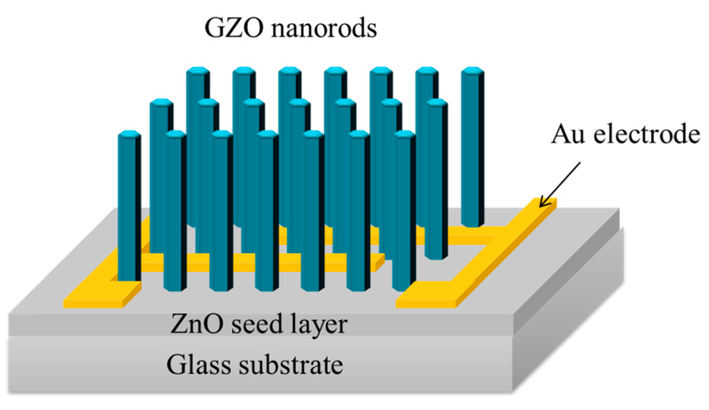
Figure 1.
Schematic diagram of the fabricated GZO nanorod photodetector. The GZO nanorods are grown by hydrothermal method.
The surface morphologies and crystal quality of the synthesized materials were characterized using a high-resolution scanning electron microscope (Hitachi S-4800I, Hitachi High-Technologies corporation, Tokyo, Japan) and a high-resolution transmission electron microscope (HRTEM, Philips Tecnai F20 G2 FEG-TEM, Philips, Eindhoven, the Netherlands). X-ray diffractometer (XRD, Bruker D8 advance, Bruker, Germany) was used to characterize the crystallographic and structural properties of the grown GZO nanorods. The optical property of the samples were analyzed by a photoluminescence (PL) measurement system which was made at RT using a He-Cd laser (325 nm, 5 mW) as the excitation light source. A Keithley 2410 semiconductor parameter analyzer was then used to measure the I-V and photodetector characteristic of the fabricated device. The spectral responsivity of the photodetector was measured using a Jobin Yvon-Spex system with a 300 W xenon arc lamp light source (Perkin Elmer PE300BUV, PerkinElmer, Foster City, CA, USA) and a standard synchronous detection scheme measured at 300 Hz.
3. Results and Discussion
Figure 2a,b show GZO nanorods have a well-aligned shape in the vertical direction as seen in the top-view and cross-section SEM image. Figure 2a indicates that the average diameters of the GZO were around 54 and 49 nm, and Figure 2b shows that average lengths were 1.96 and 1.28 μm, respectively. According to a previous report, the growth mechanism that explains this chemical reaction is as follows:
(CH2)6 N4 + 6H2O → 6HCHO + 4NH3
NH3 + H2O ↔ NH4+ + OH-
Zn2+ + 2OH-→Zn(OH)2
During this synthesis, Zn(NO3)2 and HMTA serve as a Zn2+ ion source and a pH buffer, respectively. The latter keeps the pH values ∼7. Hence, the formation of more surface defects at a lower pH is caused by the presence of more H+ ions, which absorb more OH groups and O2− ions [14,15,16,17].
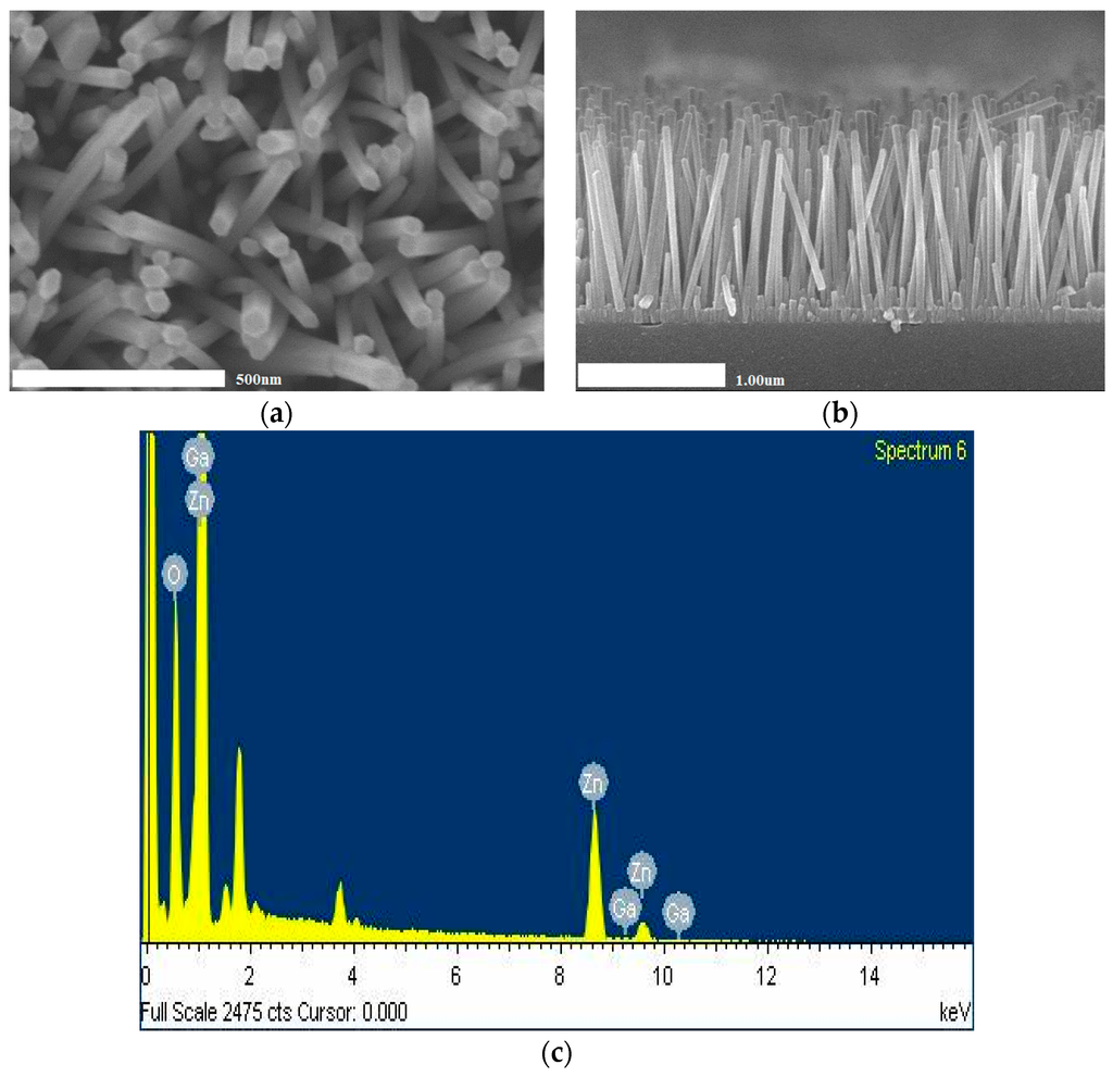
Figure 2.
This figure shows GZO nanorods have a well-aligned shape in the vertical direction as seen in the top-view (a) and cross-section (b) SEM image. (c) shows that the existence of Ga was examined by energy diffraction spectra.
Figure 2c shows that the existence of Ga was examined by energy diffraction spectra (EDS), indicating that the Ga atom entered into the ZnO lattice. It is found that the GZO contains 40.11% zinc, 56.33% oxygen and 3.57% gallium as shown in Table 1. The composition ratio of the nanorods is Ga0.008Zn0.992O which agrees well with the desired composition ratio. From the EDS, we see that no other element exists.

Table 1.
Shows the GZO nanorods contain zinc, oxygen and gallium, respectively.
| EDS | |||
|---|---|---|---|
| Element | O k | Zn L | Ga L |
| Ga-doped ZnO | 56.33% | 40.11% | 3.57% |
Figure 3 shows the structural characteristics of the GZO nanorods were measured by X-ray diffraction (XRD). It was found that the peaks related to the wurtzite structure ZnO (100), (002), and (101) diffraction peaks. The (002) peak indicates that the nanorods were preferentially oriented in the c-axis direction.
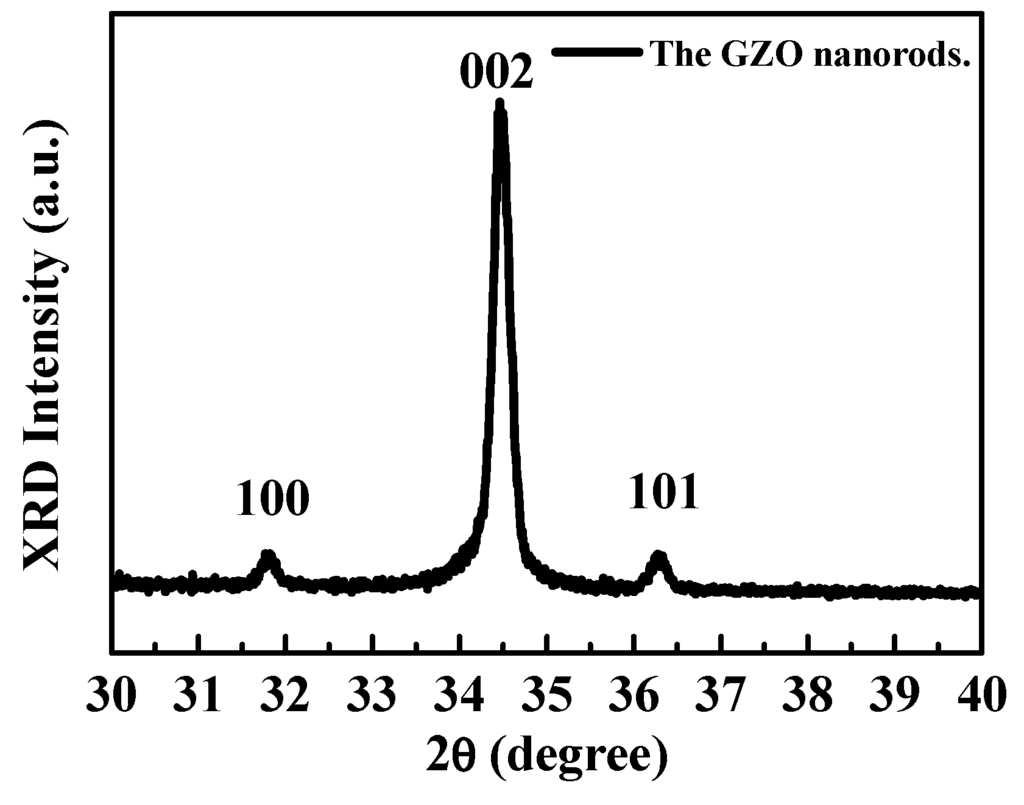
Figure 3.
The XRD pattern of the GZO nanorods.
At room temperature, Figure 4 shows the optical properties of the GZO were measured by photoluminescence spectra. It was found that the GZO nanorod arrays exhibit two different emissions, including UV (ultraviolet) and green emissions. There is a reduction in the UV peak with Ga-doping because Ga atoms enter into the lattice sites, substituting for Zn atoms, causing serious lattice distortions and leading to decreased UV emission peaks. The green emission peak at 560 nm was attributed to the existence of oxygen vacancy and interstitial in our GZO nanorods.
According to previous works, the morphology of GZO nanorods will be converted into a nanosheet along with gallium-doped concentration increases. The crystal structure of GZO nanorods indicated a reduced crystallite quality of the ZnO nanorods (NRs) due to the incorporation of Ga atoms into the ZnO lattice network [17,18,19], and our PL spectra results are in agreement with previous reports suggesting that Ga doping improves the optical properties of ZnO NR arrays [14,20].
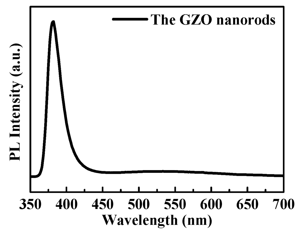
Figure 4.
Room-temperature PL spectra of GZO nanorods.
Figure 5 shows the photocurrent rise and decay by turning the UV illumination at 365 nm on and off in the air. Before the UV illumination turned on, O2 molecules adsorbed on the surface of GZO nanorods and formed O2- by capturing the free electrons of the nanorods. Hence, the phenomenon decreases not only the carrier density but also the mobility of the remaining carriers by creating depletion layers near the surface [21,22]. When UV illumination is turned on, the photocurrent rapidly increases a huge number of electric-hold pairs. It can be attributed to the holes migrating to the surface to return O2 by desorbing the O2− under UV illumination. After UV illumination is removed, the dark currents decrease by recombining electron–hole pairs [14].
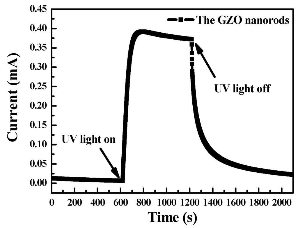
Figure 5.
GZO nanorod current-time characteristics at UV illumination.
Under UV illumination at 365 nm in the air at an applied bias of 1 V, the dark current and photocurrent of the GZO nanorod photodetector were 3.8 × 10⁻⁴ and 2.5 × 10⁻⁵ A, respectively. The photocurrent-to-dark-current contrast ratio of the fabricated photodetector exceeded 15.2.
4. Conclusions
In summary, GZO nanorods were grown on a glass substrate by using a low-temperature hydrothermal method. The GZO nanorods exhibited wurtzite structures. The dynamic response of the GZO nanorod photodetector with Au electrodes had a photo current and dark current of 3.8 × 10⁻⁴ and 2.5 × 10⁻⁵ A, respectively. The photocurrent-to-dark-current contrast ratio of the fabricated photodetector exceeded 15.2.
Acknowledgments
This work was supported by Ministry of Science and Technology under contract numbers MOST 104-2221-150-042 and MOST 103-2221-E-150-034. This work was also supported by National Science Council of Taiwan under contract numbers NSC 102-2221-E-150-046 and NSC 101-2221-E-150-043. The authors would like to thank the Common Laboratory for Micro/Nano Science and Technology, National Formosa University, for providing the partial equipment for measurement. They would also like to thank the Center for Micro/Nano Science and Technology, National Cheng Kung University, for the assistance in device characterization.
Author Contributions
Sheng-Joue Young conceived and designed the experiments; Chia-Lin Chiou and Yi-Hsing Liu performed the experiments; Liang-Wen Ji participated in data analysis. All authors read and approved the final manuscript.
Conflicts of Interest
The authors declare no conflict of interest.
References
- Ji, L.W.; Peng, S.M.; Su, Y.K.; Young, S.J.; Wu, C.Z.; Cheng, W.B. Ultraviolet photodetectors based on selectively grown ZnO nanorod arrays. Appl. Phys. Lett. 2009, 94, 203106-1–203106-3. [Google Scholar] [CrossRef]
- Ahsanulhaq, Q.; Umar, A.; Hahn, Y.B. Growth of aligned ZnO nanorods and nanopencils on ZnO/Si in aqueous solution: Growth mechanism and structural and optical properties. Nanotechnology 2007, 18, 115603-1–115603-7. [Google Scholar] [CrossRef]
- Kulkarni, A.J.; Zhou, M.; Ke, F.J. Orientation and size dependence of the elastic properties of zinc oxide nanobelts. Nanotechnology 2005, 16, 2749–2756. [Google Scholar] [CrossRef]
- Shen, X.P.; Yuan, A.H.; Hu, Y.M.; Jiang, Y.; Xu, Z.; Hu, Z. Fabrication, characterization and field emission properties of large-scale uniform ZnO nanotube arrays. Nanotechnology 2005, 16, 2039–2043. [Google Scholar] [CrossRef] [PubMed]
- Li, C.; Fang, G.J.; Su, F.H.; Li, G.H.; Wu, X.G.; Zhao, X.Z. Synthesis and photoluminescence properties of vertically aligned ZnO nanorod-nanowall junction arrays on a ZnO-coated silicon substrate. Nanotechnology 2006, 17, 3740–3744. [Google Scholar] [CrossRef]
- Wan, Q.; Li, Q.H.; Chen, Y.J.; Wang, T.H.; He, X.L.; Li, J.P.; Lin, C.L. Fabrication and ethanol sensing characteristics of ZnO nanowire gas sensors. Appl. Phys. Lett. 2004, 84, 3654–3656. [Google Scholar] [CrossRef]
- Liang, S.; Sheng, H.; Liu, Y.; Hio, Z.; Lu, Y.; Shen, H. ZnO Schottky ultraviolet photodetectors. J. Cyst. Growth 2001, 225, 110–113. [Google Scholar] [CrossRef]
- Huang, M.; Wu, Y.; Feick, H.; Tran, N.; Weber, E.; Yang, P.D. Catalytic growth of zinc oxide nanowires by vapor transport. Adv. Mater. 2001, 13, 113–116. [Google Scholar] [CrossRef]
- Choi, J.H.; Tabata, H.; Kawai, T. Initial preferred growth in zinc oxide thin films on Si and amorphous substrates by a pulsed laser deposition. J. Cyst. Growth 2001, 226, 493–500. [Google Scholar] [CrossRef]
- Ambia, M.G.; Islam, M.N.; Hakim, M.O. The effects of deposition variables on the spray pyrolysis of ZnO thin film. J. Mater. Sci. 1994, 29, 6575–6580. [Google Scholar] [CrossRef]
- Saito, N.; Haneda, H.; Sekiguchi, T.; Ohashi, N.; Sakaguchi, I.; Koumoto, K. Low-temperature fabrication of light-emitting zinc oxide micropatterns using self-assembled monolayers. Adv. Mater. 2002, 14, 418–420. [Google Scholar] [CrossRef]
- Lee, J.Y.; Choi, Y.S.J.; Kim, H.; Park, M.O.; Im, S. Optimizing n-ZnO/p-Si heterojunctions for photodiode applications. Thin Solid Films 2002, 403–404, 550–557. [Google Scholar] [CrossRef]
- Hsieh, Y.P.; Chen, H.Y.; Lin, M.Z.; Shiu, S.C.; Hofmann, M.; Chern, M.Y.; Jia, X.T.; Yang, Y.J.; Chang, H.J.; Huang, H.M.; et al. Electroluminescence from ZnO/Si-Nanotips light-emitting diodes. Nanoletters 2009, 9, 1839–1843. [Google Scholar] [CrossRef] [PubMed]
- Wang, H.H.; Baek, S.; Song, J.J.; Lee, J.; Lim, S.W. Microstructural and optical characteristics of solution-grown Ga-doped ZnO nanorod arrays. Nanotechnology 2008, 19, 075607-1–075607-6. [Google Scholar] [CrossRef] [PubMed]
- Hsiao, C.H.; Huang, C.S.; Young, S.J.; Chang, S.J.; Guo, J.J.; Liu, C.W.; Yang, T.Y. Field-emission and photoelectrical characteristics of Ga–ZnO nanorods photodetector. IEEE Trans. Electron Devices 2013, 60, 1905–1910. [Google Scholar] [CrossRef]
- Ma, S.; Fang, G.J.; Li, C.; Sheng, S.; Fang, L.G.; Fu, Q.; Zhao, X.Z. Controllable synthesis of vertically aligned ZnO nanorod arrays in aqueous solution. J. Nanosc. Nanotechnol. 2006, 6, 2062–2066. [Google Scholar] [CrossRef]
- Li, Q.C.; Kumar, V.; Li, Y.; Zhang, H.T.; Marks, T.J.; Chang, R.P.H. Fabrication of ZnO nanorods and nanotubes in aqueous solutions. Chem. Mater. 2005, 17, 1001–1006. [Google Scholar] [CrossRef]
- Wang, B.Q.; Xia, C.H.; Iqbal, J.; Tang, N.J.; Sun, Z.R.; Lv, Y.; Wu, L. Influences of Co doping on the structural, optical and magnetic properties of ZnO nanorods synthesized by hydrothermal route. Solid State Sciences 2009, 11, 1419–1422. [Google Scholar] [CrossRef]
- Hong, H.S.; Chung, G.S. Humidity sensing characteristics of Ga-doped zinc oxide film grown on a polycrystalline AlN thin film based on a surface acoustic wave. Sens. Actuators B: Chem. 2010, 150, 681–685. [Google Scholar] [CrossRef]
- Phan, D.T.; Farag, A.A.M.; Yakuphanoglu, F.; Chung, G.S. Optical and photoluminescence properties of Ga doped ZnO nanostructures by sol–gel method. J. Electroceram. 2012, 29, 12–22. [Google Scholar] [CrossRef]
- Ahn, C.H.; Han, W.S.; Kong, B.H.; Cho, H.K. Ga-doped ZnO nanorod arrays grown by thermal evaporation and their electrical behavior. Nanotechnology 2009, 20, 015601-1–015601-7. [Google Scholar] [CrossRef] [PubMed]
- Li, Y.B.; Valle, F.D.; Simonnet, M.; Yamada, I.; Delaunay, J.J. Competitive surface effects of oxygen and water on UV photoresponse of ZnO nanowires. Appl. Phys. Lett. 2009, 94, 023110-1–023110-3. [Google Scholar] [CrossRef]
© 2016 by the authors; licensee MDPI, Basel, Switzerland. This article is an open access article distributed under the terms and conditions of the Creative Commons by Attribution (CC-BY) license (http://creativecommons.org/licenses/by/4.0/).