1. Introduction
In recent decades, the widespread adoption of Commercial Off-The-Shelf (COTS) electrical, electronic, and electromechanical (EEE) components has revolutionized the development of space technologies. This shift, driven by the pursuit of cost-effective and rapid advancements, raises critical questions about the reliability of these components under harsh space conditions. In this context, Silicon Photomultipliers (SiPMs) have emerged as highly attractive detectors for various space applications due to their high photon detection efficiency (PDE), low power consumption, compact size, and immunity to magnetic fields [
1,
2]. These characteristics enable efficient operation in low-light conditions and integration into lightweight space instruments, making SiPMs ideal for missions requiring precise particle detection [
3,
4]. SiPMs have recently been employed in a wide range of space-based applications, including detection of transient gamma-ray emissions [
5], measurement of high-energy cosmic rays [
6,
7,
8,
9], and coincidence detection between gamma-ray bursts and associated gravitational wave events [
10]. Beyond space applications, SiPMs are also widely utilized in terrestrial domains, such as optical communication systems [
11] and quantum optics experiments [
12,
13].
However, the environment of space poses significant challenges for EEE components, including SiPMs, particularly due to exposure to ionizing radiation, primarily from trapped electrons and protons. Such radiation can induce defects in the silicon lattice, leading to increased dark current, while typically preserving other intrinsic properties such as gain, PDE, and breakdown voltage [
14,
15,
16]. This degradation can impair the detector’s ability to resolve single-photon events, thereby affecting overall performance during extended missions. From 2020 to 2024, we conducted an in-orbit experiment to evaluate the long-term performance of SiPMs in Low Earth Orbit (LEO), using the LabOSat-01 (LS-01) [
17] payload aboard the ÑuSat-7 satellite (COSPAR-ID: 2020-003B). Over the 1460-day mission, the four SiPMs exhibited a progressive increase in dark current—up to a factor of 500—consistent with the radiation-induced degradation reported in previous ground-based studies [
18,
19,
20]. Toward the end of the mission, as the satellite’s altitude decreased, a gradual increase in internal temperature was observed. At equal temperatures, a slight reduction in the residual dark current was detected, suggesting a possible annealing effect driven by temperature. These findings not only confirm the expected degradation behavior but also point to the potential of thermal recovery mechanisms [
21] under space conditions.
To mitigate cumulative radiation-induced damage, thermal annealing [
22] is a viable recovery technique. This process facilitates the recombination of defects within the crystal lattice, thereby reducing dark current and partially restoring the SiPM’s performance. Studies have shown that annealing depends on both temperature and duration, with higher temperatures resulting in faster recovery of SiPM performance [
23]. However, even at temperatures as low as 5 °C [
19,
24], some degree of passive recovery has been observed, which is particularly relevant for space applications where thermal control may be limited. Gu et al. [
25] demonstrated significant performance restoration using in situ current annealing, where localized heating was achieved by forward biasing of the device during irradiation. While effective, this method applies high current directly to the SiPM, potentially introducing additional stress or degradation. Additionally, recent studies have investigated the thermal behavior of irradiated SiPMs, highlighting the role of self-heating due to increased dark current as a potential factor influencing their performance in orbit [
26]. These findings reinforce the importance of understanding and controlling thermal effects in space-based SiPM applications, both for performance stability and for enabling recovery strategies such as annealing.
This work presents an experimental study on the irradiation of SiPMs under controlled conditions, analyzing the impact of proton-induced damage on sensor performance. A recovery method based on thermal annealing is explored to evaluate its effectiveness in restoring key electrical parameters. For this purpose, we studied different heater geometries fabricated directly on a printed circuit board (PCB). This procedure makes integration into lightweight payloads feasible. The power consumption and the energy required to restore the sensor were studied. The findings aim to inform strategies for the reliable use of SiPMs in space environments, supporting their integration into future scientific and commercial space missions.
2. Materials and Methods
The experiment was conducted at the EDRA (Ensayos de Daño por Radiación y Ambiente) [
27] facility of the TANDAR heavy-ion accelerator, located at Centro Atómico Constituyentes (CNEA) in Buenos Aires, Argentina. The TANDAR accelerator is a vertical electrostatic tandem system capable of operating with both protons and heavy ions. This facility is specifically designed to attenuate ion flux, enabling the controlled simulation of LEO radiation conditions for space-related experiments.
Within the EDRA irradiation line (
Figure 1), a 72 µm thick tantalum–copper (Ta–Cu) foil was placed 6 m from the target to attenuate the proton flux. This foil contained 100 perforations, each with an average diameter of 31 µm, enabling flux reduction by a factor of up to 1900. By applying this configuration and setting the accelerator to its lowest operational current, a proton flux of (4.9 ± 0.2) × 10
5 s
−1cm
−2 was achieved inside the vacuum chamber.
The vacuum chamber is equipped with a set of remotely controlled concentric rings, each featuring a patterned aperture system that allows the precise positioning of different structures as beam targets. These rings can be adjusted from the accelerator control room, enabling the selection of various shielding configurations or the replacement of samples under the proton beam. The chamber operates at a vacuum pressure of 10−5 bar, ensuring controlled irradiation conditions.
2.1. Heater Design
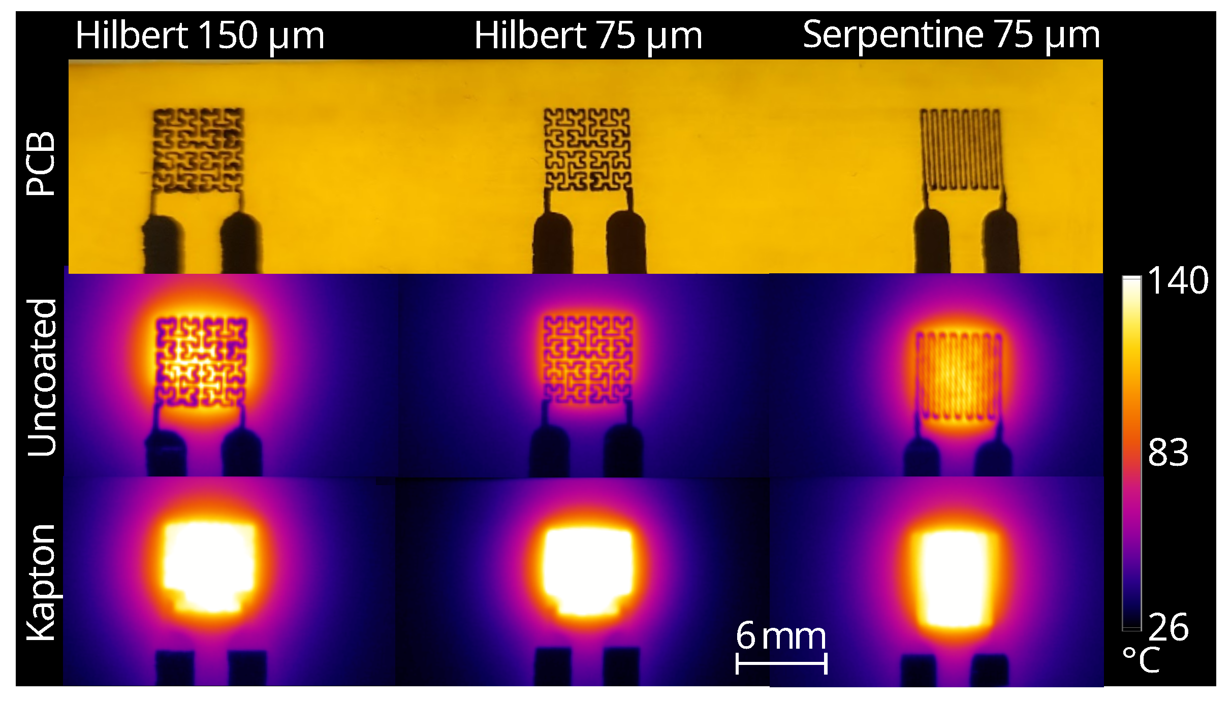
To enable controlled thermal annealing during proton irradiation, three distinct heater prototypes were designed and integrated into PCBs. The three heater prototypes were fabricated on separate PCBs, as illustrated in
Figure 2. Prior to irradiation, a comprehensive characterization of each design was conducted with the following evaluation criteria: power consumption, minimum current, and heat uniformity.
The evaluated heater designs are based on two distinct geometries: a serpentine pattern [
28] and a Hilbert curve [
29,
30]. The serpentine heater and one of the Hilbert designs were manufactured with a wire width of 75 µm, while an additional Hilbert variant was designed with a wider pitch of 150 µm.
A qualitative assessment of the heat distribution uniformity was conducted using thermographic imaging (
Figure 2). After a 50 µm thick layer of Kapton tape was applied, improved thermal uniformity was observed in the serpentine structure, as the pad corners in the Hilbert curve design exhibited uneven heat distribution. The power consumption of each heater depends on the trace resistance, which can be adjusted by modifying the trace width and length. The complete power and current consumption profiles as a function of temperature are shown in
Figure 3a and
Figure 3b, respectively. These profiles illustrate the measured electrical requirements to reach the target temperature of 100 °C for each heater design. Specifically, the figure shows that the serpentine design exhibits the lowest current requirement to reach 100 °C, while the 150 µm Hilbert geometry achieves the lowest power dissipation at the same target temperature, but with a 30% higher current. The power scales accordingly, and the difference in power is due to the difference in resistance between designs.
Based on these observations, the serpentine geometry with a 75 µm wire width was selected for subsequent irradiation experiments. This configuration exhibited the most uniform thermal distribution in thermographic analysis and demonstrated the lowest current consumption among the prototypes, making it the most suitable choice for power-constrained space applications. Satellite power systems are typically current-limited, as they rely on solar arrays and battery storage with restricted current delivery capabilities. Although the total power dissipation also depends on the heater’s resistance, the current demand directly impacts the sizing and stability of satellite power regulation systems. By minimizing current consumption, we reduce the electrical load on the satellite’s distribution buses, mitigate potential thermal stresses, and contribute to enhancing overall mission reliability and operational lifetime.
2.2. Setup
To evaluate the effectiveness of the proposed thermal recovery technique, an experiment was designed in which two MICROFC-60035 SiPMs were irradiated together under controlled conditions. The area of each SiPM was 6 × 6 mm2, and the microcell pitch was 35 µm. The first sample (SiPM A) was coupled with the serpentine heater and underwent thermal annealing between irradiation cycles. The second sample (SiPM B) served as a control and was irradiated without any recovery process. To reduce thermal coupling, the sensors were not in immediate thermal contact. However, the shortest thermal conduction path between SiPM A and SiPM B was approximately 11 cm of FR4.
For this experiment, we selected 9 MeV protons based on TRIM (Transport of Ions in Matter) [
31] Monte Carlo simulations. This analysis showed that the proposed energy was sufficient to allow the protons to penetrate the SiPM structure and stop within the bulk silicon, depositing energy along their path. In total, eight irradiation cycles were performed, reaching a cumulative fluence of (1.89 ± 0.01) × 10
8 p/cm
2. The irradiation conditions were defined to replicate a representative radiation environment for LEO missions. According to in-orbit measurements from the LS-01 payload onboard ÑuSat-7, the cumulative 1 MeV neutron equivalent fluence received by the SiPMs and associated electronics was approximately
n/cm
2 over a four-year mission duration [
18,
19].
For 9 MeV protons, the damage equivalence factor (
) in silicon is
[
32,
33,
34], meaning that one 9 MeV proton induces roughly five times as much displacement damage as a 1 MeV neutron. Based on this, the total proton fluence applied in our experiment, which was
p/cm
2, corresponds to a neutron equivalent fluence of
n/cm
2. Using the average daily fluence reported in orbit (
n/cm
2/day [
19]), this is equivalent to approximately 278 days in LEO.
The TRIM simulation considered a multi-layer structure, consisting of the following parts: (i) a 72 µm tantalum–copper (Ta–Cu) sheet with respective Ta and Cu thicknesses of 70 µm and 2 µm, designed to attenuate the incident proton flux; (ii) a silicon oxide layer, which forms the protective coating of the sensor; and (iii) the active detection region, primarily composed of silicon.
Both SiPMs were biased at 30 V using a Keithley 2612B two-channel source measure unit (SMU), which continuously monitored their dark current throughout the experiment. SiPM A was integrated in the copper side of the heater, isolated with Kapton tape. Thermal grease was applied between the heater and the SiPM in order to improve the thermal conductivity. Its temperature was measured using a Resistance Temperature Detector (RTD) and incorporated into the feedback control loop to maintain the heater at the target temperature of 100 °C. The experimental setup is shown in
Figure 4. The annealing temperature was selected based on the higher manufacturer-specified storage temperature limit of 105 °C, aiming to maximize the recovery effect. To prevent potential damage due to high current, a current compliance limit of 138.9 µA/mm
2 (equivalent to 5 mA for the full sensor area) was set throughout the annealing process. Although the device was under a fixed reverse bias, it remained above breakdown during annealing, since the breakdown voltage increases by 1.6 V when the temperature increases from 25 °C to 100 °C (which is lower than the 5.5 V overvoltage set point at 25 °C. Previous studies with Hamamatsu SiPMs reported improved dark-current recovery at higher temperatures, such as 120 °C [
23], though such conditions surpass the specified limits for the devices used in this work. The heating duration was set to 5 min for the first six irradiation cycles and extended to 10 min in the seventh cycle. During each thermal annealing cycle, SiPM A remained under a reverse bias. Before the start of each new irradiation interval, the system was allowed to cool down until the SiPM temperature stabilized within the range of 27 °C to 30 °C.
2.3. Definitions
To quantify the degradation and the effectiveness of thermal annealing, we define two metrics: the slope of degradation and the recovery factor.
The slope of degradation (
S) represents the mean increase in dark current due to irradiation normalized to the area of the SiPM and the 1 MeV equivalent fluence and is given by
where
and
are the dark currents measured before and after each irradiation interval, respectively;
is the 1 MeV equivalent fluence applied in the irradiation interval; and A is the sensor area.
The recovery factor (
R) quantifies the dark-current reduction due to annealing and is defined as
where
is the dark current measured after the annealing cycle.
3. Results
In this section, the main experimental results are presented, focusing on the effects of proton irradiation and thermal annealing on the performance of the SiPMs. The analysis includes the evolution of dark current, the influence of temperature, and variations in the breakdown voltage. Comparisons are made between the annealed and non-annealed samples, highlighting the impact of thermal recovery processes on radiation-induced degradation.
3.1. Dark Current
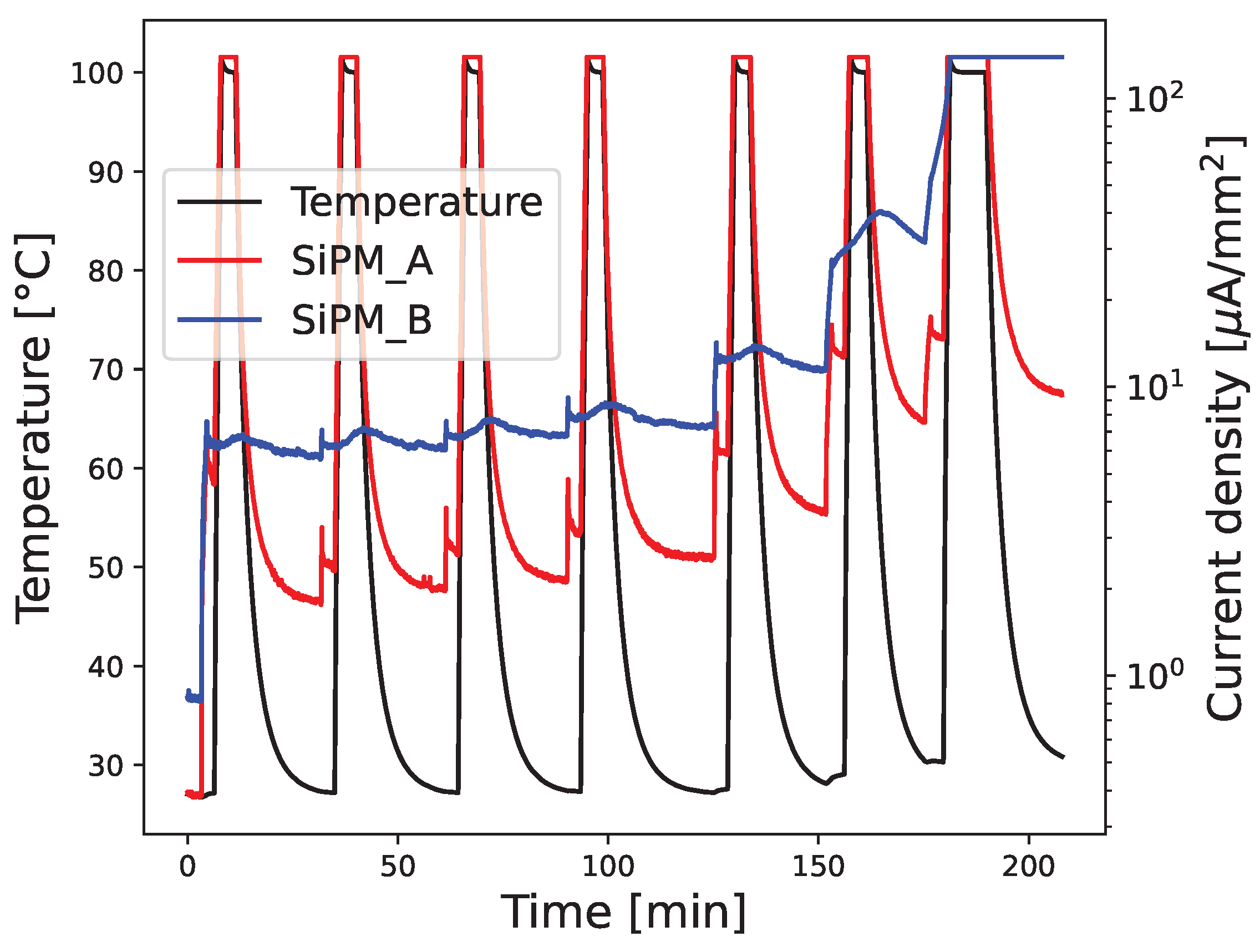
Performing real-time measurements and thermal annealing in situ inside the irradiation chamber enables the continuous tracking of damage to the SiPM.
Figure 5 illustrates the irradiation process, with highlighted regions indicating the moments when thermal annealing was applied to SiPM A. A progressive reduction in dark current is observed in SiPM A following each thermal cycle, suggesting a partial recovery effect induced by temperature. The results obtained for the degradation (Equation (
1)) and recovery (Equation (
2)) metrics are summarized in
Table 1.
However, it is important to consider potential factors that may have influenced the behavior of SiPM B. For instance, thermal coupling between the two sensors could have resulted in partial heat transfer during the annealing cycles of SiPM A. This effect appears to have led to a temperature increase of less than 10 °C in SiPM B, which may have contributed to a slight recovery of its dark current, as seen in the small current jumps of sample B between cycles.
Figure 6 shows the continuous dark-current measurement at a fixed bias of 30 V, along with the temperature of sensor A recorded throughout the experiment. The plot highlights both the irradiation periods and the thermal cycles. Owing to the intrinsic dependence of dark current on temperature, an increase in the dark current of SiPM A is observed when the heater is activated, reaching the compliance limit. A slight increase in the dark current of SiPM B is also observed, likely caused by thermal coupling between the sensors.
A recovery of at least 39% was achieved, regardless of the cumulative fluence, demonstrating the effectiveness of the thermal annealing process across multiple irradiation levels. The mean irradiation degradation slope varied from approximately 3 to µA/(mm2) across different cycles. The difference in slope between different cycles may be due to annealing-induced recombination of certain defects and is influenced by the statistical uncertainty of S (which is on the order of µA/(mm2)). The most significant annealing recovery occurred during the first irradiation cycle, suggesting that applying the thermal annealing process at lower fluence intervals is necessary, after which the recovery remains approximately constant throughout subsequent irradiation and annealing cycles. The control sensor (SiPM B) exhibited a continuous increase in dark current, eventually reaching saturation. However, after being subjected to bias voltage power cycling (i.e., the bias voltage was temporarily turned off and then re-applied) and a temperature increase, the sensor regained functionality, stabilizing at a dark current of 17 µA/mm2 at 30 °C.
3.2. Current and Temperature
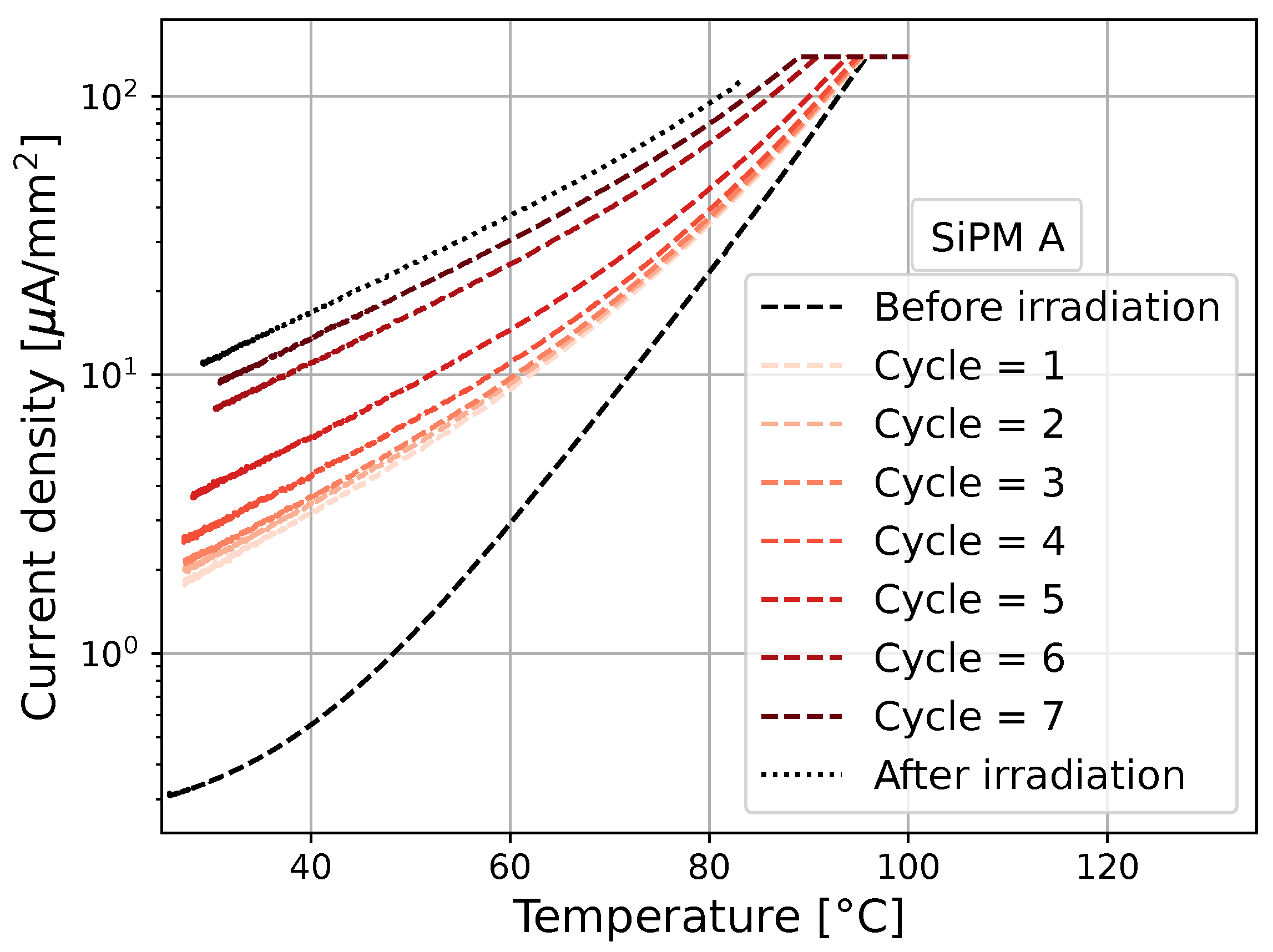
The behavior of SiPM A following each thermal annealing cycle was analyzed.
Figure 7 presents the dark-current measurements for SiPM A at different temperatures, including values before irradiation, after each irradiation cycle, and one month after irradiation. The fundamental operating behavior of the sensor remained unaffected by radiation exposure. While the dark current increased due to radiation-induced degradation, the sensor continued responding as expected, exhibiting the characteristic increase in dark current with rising temperature.
For the control sample (SiPM B), which did not undergo significant thermal annealing, the radiation-induced degradation is shown in
Figure 8. This device showed a progressive increase in dark current. After each thermal annealing step of SiPM A, a slight current reduction was observed in SiPM B. This effect could be explained by thermal coupling between the two devices. Nonetheless, in cycles 6 and 7, SiPM B exhibited a constant increase in dark current even when outside the periods of irradiation and heating of SiPM A. This behavior continued until the SiPM reached the current limit and stopped working.
Figure 8 also illustrates the recovery behavior of SiPM A after each annealing cycle, in comparison with the corresponding current evolution of SiPM B throughout the irradiation sequence. The results show a consistent and pronounced decrease in SiPM A’s dark current after each thermal cycle, confirming the effectiveness of the applied annealing procedure.
3.3. Breakdown Voltage
The breakdown voltage (V
B) was analyzed before and after irradiation to assess potential radiation-induced changes. This parameter was estimated by measuring the dark current as a function of bias voltage at room temperature (25–26 °C). The results are presented in
Figure 9. No significant differences were observed in V
B between pre- and post-irradiation conditions. Prior to irradiation, the breakdown voltage was measured as (24.63 ± 0.16) V for SiPM A and (24.47 ± 0.16) V for SiPM B. After irradiation, both sensors exhibited a breakdown voltage of (24.64 ± 0.09) V, indicating that irradiation did not significantly alter this parameter. The value of V
B was determined using the second derivative method applied to the dark-current curve, following the approach described in [
35], and the error bars were defined based on the voltage step size used in the measured I–V curves. The pre-irradiation measurements were performed in a custom-built vacuum chamber. A leakage current affecting some of the measurement channels used for the pre-irradiation SiPM I–V curves was identified a posteriori. This additional current (approximately 50 nA for SiPM A and 10 nA for SiPM B) is attributed to that leakage, and this offset current is small enough that it does not affect the determination of
. Measuring the breakdown voltage under vacuum conditions was essential to replicate the irradiation environment of the SiPMs. The post-irradiation I–V curves were measured in situ within the irradiation vacuum chamber (these were performed one month after irradiation, during which both devices remained at room temperature), and so no leakage current was observed in these measurements.
4. Discussion
In this study, we investigated the effects of proton irradiation on SiPMs and explored thermal annealing as a potential recovery technique for space application. Two SiPMs were irradiated under controlled conditions. One sensor underwent thermal cycling from 27 °C up to 100 °C in between irradiation intervals, while the other served as a control sample without any recovery. Both sensors were biased at a constant voltage of 30 V throughout the experiment. The experiment was designed to simulate radiation damage in LEO and assess the feasibility of in-flight recovery strategies using a PCB-integrated heater.
For satellite applications, minimizing current consumption is critical due to strict power generation constraints and limited heat dissipation capabilities. Based on thermal image analysis and electrical measurements, the 75 µm wide serpentine geometry was selected because it achieved the best heat distribution and the lowest current requirement among the tested heater designs.
The results demonstrate that thermal annealing can significantly mitigate radiation-induced degradation. A dark current recovery of over 39% was achieved with only 5 min of thermal cycling at 100 °C, highlighting the effectiveness of low-temperature annealing in restoring sensor performance. This is particularly promising for small satellite missions, as it suggests that in-orbit recovery of degraded SiPMs can be achieved with minimal energy and hardware complexity.
Figure 7 shows that the dark current exhibits a clear dependence on both temperature and irradiation level, increasing with each at constant bias voltage.
Additionally, no significant variations were observed in the breakdown voltage before and after irradiation and thermal cycling, reinforcing that the core operating characteristics of the SiPMs were not compromised. These findings confirm that thermal annealing is a viable, low-complexity mitigation strategy to extend the operational lifetime of SiPM-based detectors in LEO.
In contrast to the in situ current annealing approach proposed by Gu et al. [
25], our method decouples the heating mechanism from the sensor itself. By using an external PCB-integrated heater, we enable controlled thermal recovery without electrically stressing the SiPM, reducing the risk of damage. This design is more robust and better suited for small satellite platforms, where power budgets and device protection are key considerations. Recent findings on self-heating in irradiated SiPMs [
26] further emphasize the importance of controlled thermal management in orbit.
Future work will focus on optimizing the annealing profile, including temperature and duration, and validating this recovery approach across different SiPM architectures and radiation conditions. The insights gained in this study contribute to the development of resilient photodetection systems for next-generation space missions.


 ,
, 


